Nova N13072 User manual

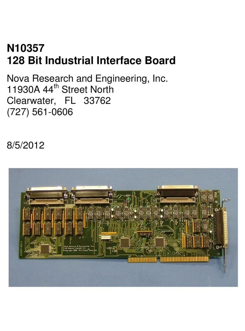
N13072
ADS168
12-Bit Analog Industrial Interface Board
Nova Research and Engineering, Inc.
11930A 44
th
Street North
Clearwater, FL 33762
(727) 561-0606
6/17/2010

ADS168 Analog Industrial Interface Board
2
Products manufactured by Nova Research and Engineering, Inc. (NRE), Clear
water,
Florida are warranted against defects in materials and workmanship for a period of one
year from the original date of delivery. Factory reconditioned and refurbished products
are warranted against defects in materials and workmanship for a period of
90 days from
the date of delivery.
This warranty does not cover damage from, or failure attributable to, acts of nature,
abuse, misuse, improper usage, faulty installation, or any modifications not expressly
authorized in writing by NRE.
NRE will repair or replace, at our option, any product determined to be defective within
the terms of this warranty. After the warranty period, charges will be rendered for any
repairs, adjustments or upgrades made to the product by NRE, including, but not limited
to,
charges for shipping, insurance, parts and labor.
NRE is not responsible or liable for indirect, special, or consequential damages arising
out of, or in connection with, the use or performance of any NRE products. NRE is not
responsible or liable for other damages with respect to loss of property, loss of revenues
or profit, or costs of removal, installation or reinstallation.
Except as provided herein, NRE makes no express warranties, and any implied
warranty, including warranties of merchantability or fitness for a particular purpose, is
limited to a period of ninety days from the original date of delivery.
This warranty gives you specific legal rights. You may have additional rights that vary
from state to state.
Rev A (printed Jan 1999)
Rev
B (printed
Ju
ne
2009)
Rev C (printed June 2010)
Robotrol and ADA88 are trademarks of Robotrol Corporation.
IBM is a registered trademark of International Business Machines.
Windows and Windows 3.1 are trademarks of Microsoft Corporation.
No part of this publication may be reproduced, stored in a retrieval system, or
transmitted, in any form or by any means without prior written permission of Nova
Research and Engineering, Inc.
The information contained herein is subject to change without notice.
Copyright (c)
1999
-
2010
by Nova R
esearch and Engineering, Inc. (USA).
All rights reserved.

ADS168 Analog Industrial Interface Board
3
Table of Contents
1
Introduction...............................................................................................
4
2
Installation..................................................
...............................................
5
2.1
Card Configuration....................................................................................
5
3
Operation....................................................................................
..............
7
Board Initialization ................. .............................................. 9
Input Programming ...................................... ......... 9
Analog Output Programming .. .. ............ .....
....
11
4
Calibra
tion.........................
.
.......................................................................
14
4
.1
Output Calibration
.................. ..............................................
14
5
Troubleshooting..................
.
.....
.................................................................
15
Appendix A
Card Specifications.......................................................................
16
Appendix B
Ordering and Service Information .....................................
.........
18
Appendix C
Programming Examples . ..... ............................................... 19
Appendix D
Interface Connections . ..... ............................................... 24

ADS168 Analog Industrial Interface Board
4
SECTION 1
Introduction
The ADS168 is a multifunction analog and digital I/O expansion board for ISA compatible
computers. The ADS168 board installs internally in a full-length expansion socket in an active or
passive backplane, and is addressed through the computer s I/O address space (no memory-
mapped addressing is supported). All analog and digital I/O is provided through a single 37-
pin,
D-
sub style female connector. The command protocol is backwardly compatible with the Robotrol
ADA88 analog expansion card. The ADS168 has been designed to provide years of reliable
performance in the most demanding, real
-
world control applications.
ADS168 Features. The ADS168 features sixteen analog inputs, eight analog outputs and 8 bits
of digital I/O. The board has a software selectable full-scale analog output voltage range of 5 or
10 VDC, software programmable variable gain input amplifier, ISA bus compatibility, and a high-
speed FIFO bus interface.
Analog Inputs. The sixteen analog inputs are single-ended (non-differential) and are converted
by a 12-bit analog-
to
-digital converter (ADC) circuit. The input amplifier has a software
programmable gain stage allowing gain settings of x1 (10VFS), x2 (5VFS), x4 (2.5
VFS
), or x8
(1.25VFS)
. The A/D converter can perform one conversion per command or can continuously
scan the analog inputs. The analog inpu
ts can be digitally filtered via an on
-
board microprocessor
(factory installed option).
Analog Outputs. There are eight 12-bit unipolar analog outputs capable of up to +10 VDC
range. Each output has a software selectable range of 5 or 10 VDC full-scale. Each output is
capable of sinking or sourcing 5 mA. Two analog outputs can be configured for up to 80 mA of
drive current (factory installed option).
Digital I/O. The eight-bit, bi-directional digital I/O port is TTL compatible. With a high-
voltage
digi
tal interface option, four bits are configured as 24 VDC open-collector output drivers and four
bits are configured as optically isolated inputs, requiring an active low signal.
ISA Bus Interface. The ISA bus interface uses high-speed CMOS logic which allows the host
system external I/O bus to run at maximum speed without the need for I/O expansion bus wait
states.

ADS168 Analog Industrial Interface Board
5
SECTION 2
Installation
The ADS168 can be installed any 16 bit slot of an ISA compatible computer system, with an
active or passive backplane. When installing or removing the board, always use ESD handling
precautions.
The card is secured using a single screw to the computer rear card frame, as shown in Figure 1,
below. Any mix of cards may be plugged in, so long as the card addresses do not overlap. The
card address must be set before installation, and this process is described in Section 2.2, below.
The electrical and environmental specifications are shown in Section 5.
Figure
1
Cards secured in cardrack
2.1
Card
Configuration
The board uses
four
of the addresses in one segment of the configured base address. Thus if the
base address is set to 320H, the board uses addresses 320H through 323
H.
Utilization of the
address is shown in Table 2.1.
I/O Address Register
Data
Direction
Function
addr + 0 INP DATA
Write
8 bit data transfer register
addr + 0 OUT DATA Read 8 bit data transfer register
addr + 1
COMMAND
Write
Command register
addr + 1
STATUS
Read Status register
addr +2 or addr +3
FIFO
Read 256 byte output data FIFO
Table 2.1
- I/O address map
The base address of the board is set using jumpers W3 (bottom, right of board), and they
configure the bits 2 through 9 of the address in the computer I/O space. Normal configuration is
3XXH
or
2XXH
.
All of the analog and digital I/O functions of the ADS168 are software configurable and do not
require additional jumper settings. The base address and interrupt (IRQ) settings are the only
options that require jumper configuration.
Base I/O Address. The board base I/O address is set by jumper block W3 (
Table
2.1). The
board uses four sequential I/O locations and can be placed at any I/O base address from 000H to
3FCH, in four-byte increments. The factory setting for the base address is 0300H. Typical
settings are shown below:

ADS168 Analog Industrial Interface Board
6
300H
304H
308H
30CH
310H
.
.
A2
X X X
.
.
A3
X
X
X
.
.
A4
X
X
X
X
. .
A5
X
X
X
X
X
. .
A6
X
X
X
X
X
. .
A7
X
X
X
X
X
.
.
A8
.
.
A9
W3
X = Jumper installed
Table 2.1
-
W3 Base I/O Address Settings
Several address settings are shown in the following photographs (Figure 2). The progression is
binary.
Address=0x300
Address=0x30
4
Address=0x30
8
Address=0x30C
Address=0x3
10
Figure 2 Some address settings
Interrupts.
The ADS168 can be configured to generate a host CPU interrupt (IRQ) when the
output buffer full (OBF) bit is set in the status register. The board can generate an interrupt on
IRQ 3, 4, 5, 6, 7, 10, 11, 12, 14, or 15 (see Table 2.2). By installing a jumper on W1 or W2, an
interrupt will be generated once the board is initialized and an A/D request has been processed.
To disable the interrupt feature, remove the IRQ jumper from W1 or W2. The factory default
setting is NO IRQ
(no jumpers installed)
.

ADS168 Analog Industrial Interface Board
7
.
.
IRQ14
.
.
IRQ7
.
.
IRQ15
.
.
IRQ6
.
.
IRQ12
.
.
IRQ5
.
.
IRQ11
.
.
IRQ4
.
.
IRQ10
.
.
IRQ3
W1 W2
Table 2.2
-
W1, W2 IRQ Jumper Settings
Use only one IRQ setting for each board in the host system. Refer to Chapter 6 for more
information on host system IRQ settings and problem sol
ving.
A photograph of the card showing
W1 and W2 is shown below (Figure 3)
.
Figure 3 W1 and W2 Connectors
Input and Output Connections. All analog and digital I/O is performed through the J1
connector. The J1 connector is a 37 pin D-
sub
miniature, jack (female) style connector. An
additional 38 pin header connector can be provided at J2 for analog and digital ground
connections (factory option). Refer to Appendix D for more information on interface signals and
locations.

ADS168 Analog Industrial Interface Board
8
SECTION 3
O
peration
This section describes the command, status and data formats for programming the ADS168. All
data is transferred in 8
-
bit I/O bus transfers to and from registers on the ADS168.
I/O Address Map. The ADS168 uses four sequential host system I/O locations starting at the
base address, as determined by the W3 jumper block (Refer to section 2.2.1). Memory mapping
is not supported. The four special function registers and the FIFO interface that occupy the four
address locations are shown in Table 3.1. The registers at offset 0 and 1 are used for both
input and output data. The FIFO is read
-
only from the ISA bus.
Power
-On Initialization. After the host system generates a power-on reset (POR) signal, all of
the analog output channels will be init
ialized to 0 VDC and the board will enter an idle mode. The
board must be initialized after the hardware reset before any of the analog or digital functions can
be used. To initialize the board, a standard mode reset command (section 3.5), followed by an
analog output initialization command (section 3.6) should be sent to the board.
I/O Address
Register
Data
Direction
Function
addr + 0
INP DATA
Write 8 bit data transfer register
addr + 0
OUT DATA
Read
8 bit data transfer register
addr + 1
COMMAND
Write Command register
addr + 1
STATUS
Read
Status register
addr +2 or addr +3
FIFO
Read
256 byte output data FIFO
Table 3.1
- I/O address map
STATUS register
7 6 5 4 3 2 1 0
1 0 0 0 0
RH
IBF
OBF
Table 3.2
- STATUS register flags
The Status Register. Before commands or data can be written into the COMMAND or INP
DATA registers, the input buffer full (IBF) flag must be clear. Before sending data to these
registers, read the STATUS register (Table 3.2) until bit 1 is reset. If data is written to the board
while the IBF flag is set, data may be lost, or the board may perform in an unpredictable m
anner.
The RH and OBF flags are detailed in other sections of this manual. Bit 7 will always be set and
can be used to identify the board as an ADS168. When reading a Robotrol ADA88, bit 7 will
always be cleared.
COMMAND register
7
6
5
4
3
2
1
0
0
0
1
1
0
0
1
0
Table 3.3 - Software reset (cleared outputs)
Standard Mode Reset. In the standard reset mode, a software reset command should precede
all other commands, after power-on reset or when restarting the board. There are two forms of
the standard mode software reset command - cleared analog outputs and analog outputs remain
unchanged. Writing a 30H or 31H to the COMMAND register (Table 3.3) will cause the board to
enter a reset state, without clearing the analog outputs. Writing a 32H to the COMMAND register
will cause the board to enter a reset state, with the anal
og outputs cleared to 0 VDC. A 30H, 31H

ADS168 Analog Industrial Interface Board
9
or 32H software reset command can be used at any time. The reset action of the 30H and 31H
commands are identical.
Board Initialization. Once the board has been reset, it will need to be initialized with the anal
og
output channel update configuration. To initialize the analog outputs, determine the number of
the last analog output channel that needs to be updated
, from 0 to 7, for a total of eight channels
.
Write this value to the COMMAND register, only after a
software or hardware reset. Note that the
IBF flag will need to be checked, prior to writing the initialization command byte to the board
. The
maximum channel number (0 to 7) determines how many of the analog outputs are to be
refreshed by the on-board microprocessor. The lower the maximum number, the higher the
possible update rate. The allowable values for the channel numbers are 00H through 07H.
COMMAND register
7 6 5 4 3 2 1 0
0 0 0 0 0 n n n
Table 3.4- Analog output initialization
Compatibility Mode Reset. Another reset mode is available to maintain backward compatibility
with software written for earlier Robotrol ADA88 boards. Like the standard mode reset, there are
two forms of the compatibility mode software reset command
-
cleared analog outputs and analog
outputs remain unchanged. Writing a 01H to the COMMAND register will cause the board to
enter a reset state, without clearing the analog outputs. Writing a 03H to the COMMAND register
will cause the board to enter a reset state, with the analog outputs cleared to 0 VDC. An 01H or
03H software reset command can be used only after the board has been initialized with an
initialization command byte. It is not recommended that the 01H or 03H software reset
commands be used for new software designs. Note that the compatibility mode reset can only be
used
after
the board has been initialized with an initialization command, following a power-
on
reset.
Analog Input Programming. The ADS168 has two analog input modes. In the single
conversion mode, the board does one analog conversion per command. In the c
ontinuous
conversion mode, selected input channels are continuously scanned and converted. The
continuously converted values are loaded into the bus interface FIFO when commanded.
Single Conversion Mode. When a single analog input conversion is to be performed, a
command byte, containing the command mode bits (D6, D7), the gain setting for the channel (D4,
D5) and the analog input channel number (D0-D3), is written to the command register. Gain
values of X1, X2, X4 and X8 can be selected as shown in t
he following table.
COMMAND register
7 6 5 4 3 2 1 0
0 1
G1
G2
MSB
- -
LSB
Gain
X1
0 0
Channel Number
X2
0 1
X4
1 0
X8
1 1
Table 3.5
- Analog Input Command
Once the conversion is complete, a 02H is loaded into the OUT DATA register, indicating that
there are two data bytes in the bus interface FIFO (Table 3.6). The first FIFO data byte contains
the channel number and the LSB data from the A/D conversion. The second FIFO data byte
contains the MSB data from the A/D conversion. The OBF flag of the STATUS register is then
set, and an ISA bus interrupt is generated, if enabled. Data can be read from the FIFO at
anytime, once the OBF flag has been set. The OBF flag and the ISA interrupt are cleared upon
ADS168 Analog Industrial Interface Board
10
the OUT DATA register being read. Data in the FIFO will be overwritten, once a new conversion
command is requested.
OUT DATA register
7 6 5 4 3 2 1 0
0 0 MSB - - - -
LSB
Byte Count in FIFO (02H)
FIFO (1st byte)
7 6 5 4 3 2 1 0
D3
D2
D2
D0
MSB
- -
LSB
Conversion Data
Channel Number
FIFO (2nd byte)
7 6 5 4 3 2 1 0
D11
D10
D9
D8
D7
D6
D5
D4
Conversion Data
Table 3.6- Single Conversion Data
The recommended
program sequence for a single channel analog input conversion is:
1. Read the STATUS register until the IBF flag is cleared.
2. Load the COMMAND register with the single conversion command byte.
3. Poll the STATUS register, checking the OBF flag or wait f
or an ISA interrupt.
4. Read the OUT DATA register to get the number of bytes in the FIFO. This action will clear the
OBF flag.
5. Read the FIFO to get the LSB of the conversion data.
6. Read the FIFO to get the MSB of the conversion data.
Continuous Conversion Mode. The ADS168 can be programmed to selectively scan the
analog inputs continuously. Each channel to be scanned must be sent to the board by an
individual continuous conversion command. The command format is similar to the single
conversion mo
de command, with the exception of the command bits (D6, D7).
COMMAND register
7 6 5 4 3 2 1 0
1 1
G1
G2
MSB
- -
LSB
Gain
X1
0 0
Channel Number
X2
0 1
X4
1 0
X8
1 1
Table 3.7- Continuous Conversion Command
Each continuous conversion command sent to the board adds an analog input channel, and a
gain setting for that channel, to an internal list of inputs to be scanned and updated. This allows
inactive or unused channels to be skipped during the scanning process. Once all of the desired
channels have been sent to the board, a single command will cause the ADS168 to load the FIFO
with the conversion data for each of the se
lected channels.
COMMAND register
76543210
00010000
Table 3.8
- Load FIFO Command

ADS168 Analog Industrial Interface Board
11
Upon receiving a load FIFO command, the ADS168 will transfer all of the current conversion data
for the selected analog input channels to the FIFO. The FIFO data will be loaded sequentially
from the lowest chan
nel number to the highest channel number in the internal scan list
-
not in the
order the list was created. In the continuous conversion mode, the FIFO data is stored in the
same format as the FIFO data in the single conversion mode (Table 3.6). Once the FIFO has
been loaded, a byte will then be loaded into the OUT DATA register indicating the number of data
bytes stored in the FIFO. The OBF flag of the STATUS register is set, and an ISA bus interrupt is
generated, if enabled. Data can be read from the FIFO at anytime, once the OBF flag has been
set. The OBF flag and the ISA interrupt are cleared upon the OUT DATA register being read.
The recommended program sequence for analog input continuous conversion mode is:
1. Read the STATUS register until th
e IBF flag is cleared.
2. Load the COMMAND register with a contin
u
ous conversion command byte for the first channel.
(Perform steps 1 and 2 for up to 16 channels)
3. Send a load FIFO command.
4. Poll the STATUS register, checking the OBF flag or wait for a
n ISA interrupt.
5. Read the OUT DATA register to get the number of bytes in the FIFO. This action will clear the
OBF flag.
6. Read the FIFO to get the LSB of the conversion data for the first channel in the list.
7. Read the FIFO to get the MSB of the co
nversion data for
the first channel in the list.
8. Repeat steps 6 and 7
until the end of the data has been reached
.
If a load FIFO command is issued and the board is not in a continuous conversion mode, the
FIFO data will be cleared and a value of zero will be loaded into the OUT DATA register,
indicating that no conversion data is present in the FIFO. Data in the FIFO will be overwritten,
each time a load FIFO command is issued.
The board will exit the continuous conversion mode when a single conversion command or a
software reset command is issued. Once the board has exited the continuous conversion mode,
the list of channels that were scanned will be cleared. A new channel list will need to be loaded
each time the continuous conversion mode is starte
d.
Analog Output Programming. When an analog output is to be updated, a command byte,
containing the command mode bit (D6) and the full-scale output range select bit (D7) for the
channel, is written to the command register. Full-scale analog output ranges of 0 - 5 VDC (D7 =
1) or 0 - 10 VDC (D7 = 0) can be selected. Two data bytes are then written to the INP DATA
register. The first byte contains the lower four bits of the analog output value and the number of
the channel to be updated, ranging from 0 to 7. The second byte contains the most significant
bits of the analog output value.
The data are shown in Table 3.9
The recommended programming sequence for the analog output mode is:
1. Read the STATUS register until the IBF flag is cleared.
2. Load t
he COMMAND register with the analog output command byte.
3. Read the STATUS register until the IBF flag is cleared.
4. Load the INP DATA register with the channel number and LSB data byte.
5. Read the STATUS register until the IBF flag is cleared.
Note t
hat once the IBF flag clears, the RH flag (bit 2 of
the STATUS register) will go high indicating the board
is ready for the high byte.
6. Load the INP DATA register with the MSB data byte.

ADS168 Analog Industrial Interface Board
12
COMMAND register
7 6 5 4 3 2 1 0
x 0 0 0 0 0 0 0
0 5 VDC Scale
1 10 VDC Scale
INP DATA (1st byte)
7
6
5
4
3
2
1
0
D3
D2
D2
D0
MSB
-
-
LSB
D/A Output Data
Channel Number
INP DATA (2nd byte)
7 6 5 4 3 2 1 0
D11
D10
D9
D8
D7
D6
D5
D4
D/A Output Data
Table 3.9- Analog Output Data
Before the ADS168 can output an analog voltage value, the board has to be initialized as
described in section 3.5. Note that the number of channels that the board continuously updates
can only be changed following a software reset command or
following a hardware
reset.
Digital I/O.
Th
e digital I/O feature of the ADS168 has two options - 8 bits of bi-directional TTL or
4 bits of high-voltage output and 4 bits of optically isolated input. The programming interface for
both digital I/O options is identical, with some minor considerations
.
To send or receive data from the digital I/O port, a single command byte, containing the digital I/O
command mode bit (D3) and the direction control bit (D3), is sent to the COMMAND register. An
output data byte, is then written to the INP DATA register for digital output. In digital input mode,
data from the digital I/O port is transferred into the OUT DATA register.
Note that the digital I/O buffer that drives the J1 connector will remain in the direction of the
current digital I/O command until another digital I/O command is used that toggles the direction
bit. This is important when using control devices that required constant e
xcit
ation for proper
operation.
COMMAND register
7 6 5 4 3 2 1 0
0 0 0 0 x 0 0 0
Input 0
Output
1
INP DATA or OUTDATA
7 6 5 4 3 2 1 0
MSB
D6
D5
D4
D3
D2
D1
LSB
Digital I/O Data
Table 3.10- Digital I/O Command and Data

ADS168 Analog Industrial Interface Board
13
The programming sequence for the digital output mode is:
1. Read the STATUS register until the IBF flag is cleared.
2. Load the COMMAND register with the digital output command.
3. Read the STATUS register until the IBF flag is cleared.
4. Load the INP DATA register with the digital output data byte.
The pro
gramming sequence for the digital input mode is:
1. Read the STATUS register until the IBF flag is cleared.
2. Load the COMMAND register with the digital input command.
3. Read the STATUS register until the OBF flag is set.
4. Read the OUT DATA register to get the digital input data byte.
When using the high voltage digital interface option, there are special programming
considerations. When this option is installed, the digital I/O port is not longer bi
-
directional across
8 bits. When a digital input is performed, the lower four bits will be input data and the upper four
bits will be cleared. When a digital output is performed, the upper four bits will be output and the
lower four bits will be ignored.

ADS168 Analog Industrial Interface Board
14
SECTION 4
C
alibration
This procedure can be used to verify the performance of the ADS168, or when troubleshooting a
control system
containing
the
ADS168
. The required instrumentation
accuracy
is high, so if a
recalibration is required, the card should be returned to the manufacturer. See Appendix A
for
details.
This procedure
must
performed by trained and qualified personnel. Voltage measurements
are
made with the host computer system operating. Caution should be observed when making
measurement near energized circuits.
A
variable DC reference voltage source and a precision digital voltmeter with a minimum full-
scale range of 30 VDC and a resolution of 0.0001 VDC
is
required. These instruments should be
routinely calibrated, and preferably NIST traceable, to maintain the precision of the ADS168.
Bef
ore performing any calibration procedures on the ADS168, verify that the host computer
system is operating properly. Check that all of the DC power supply rails are within the
recommended operating parameters. Failure to follow these procedures correctly
will
result in an
improperly calibrated board.
4.1 Output
C
alibration
Zero Adjustment. Connect a digital voltmeter (DVM), set for 20 VDC, to the analog output at
channel 0 (J1, pin 5) and ground (J1, pin 5). Send an analog output command to the ADS168 to
output 0.000 VDC at channel 0. Adjust R32 until the DVM reads 0.000 VDC, to within
0.05 mV.
10 VDC Full Scale Adjustment. Send an analog output command to the ADS168 to output a
full
-scale (FFFH) voltage on the 10 VDC range. Adjust R34 until the DVM reads 9.998 VDC, to
within
0.5 mV.
5 VDC Full Scale Adjustment.
Send an analog output command to the ADS168 to output a full
-
scale (FFFH) voltage on the 5 VDC range. Adjust R33 until the DVM reads 4.999 VDC, to within
0.5 mV.
Analog Input Calibration. The following section describes how to calibrate the analog input
section of the ADS168. Note that for proper accuracy, the analog input zero adjustment must
precede the analog input gain adjustment.
Zero Adjustment.
Connect analog input channel 0 (J1, pin 13) to a 2.44 mV DC voltage source.
Read the analog input value using single conversion mode. Adjust R31 until the FIFO data value
is 001H, or reads 0.002 VDC when converted to a voltage value.
If a 2.44 mV DC voltage source is not available, the analog input channel 0 can be connected to
the analog output channel 0 (J1, pin 5) and an output command with a value of 001H (on the 10
VDC scale) can be sent to the channel 0 analog output. This should produce a 2.44 mV signal at
the channel 0 output.
Verify this voltage with the DVM before adjusting R31. If this voltage is not
correct, the analog output should be recalibrated before proceeding.
Gain Adjustment. Connect analog input channel 0 (J1, pin 13) to a 9.995 VDC voltage source.
Read the analog input value using single conversion mode. Adjust R30 until the value is FFEH,
or when converted to a voltage value the displayed value reads 9.995 VDC.
If a 9.995 VDC voltage source is not available, the analog input channel 0 can be connected to
the
analog output channel 0 (J1, pin 5) and an output command with a value of FFEH (on the 10
VDC scale) can be sent to the channel 0 analog output. This should produce a 9.995 VDC signal
at the channel 0 output. Verify this voltage with the DVM before adjusting R30. If this voltage is
not correct, the analog output should be recalibrated before proceeding.

ADS168 Analog Industrial Interface Board
15
SECTION 5
Troubleshooting
I/O Address Conflicts. When operating the ADS168 with several other I/O adapters in a
system, verify that the other I/O adapters do not share I/O address space with the ADS168.
Refer to S
ections 2.2.1 and 3.2.
Interrupt Conflicts. Interrupt conflicts are very common in ISA bus computer systems. If the
interrupt feature of the ADS168 is enabled, verify that other I/O adapter cards in the system are
not using the same interrupt. In plug-
and
-play (PNP) systems, the BIOS can reassign interrupts
during system start-up. One method to resolve PNP interrupt problems is to assign interrupts
manually in the BIOS setup. Consult your motherboard reference manual for information on
BIOS setup. Refer to S
ection 2.2.2.
Power Supply Problems. Inaccurate A/D conversion data, lack of full-scale swing of the D/A
outputs or other erratic performance of the ADS168 may be an indication of a poor power supply.
Verify that all of the DC power supply rails meet the requirements as detailed in Section 5.5
before troubleshooting other areas.

ADS168 Analog Industrial Interface Board
16
Appendix A
Technical Specifications
General.
Bus interface: ISA, 16 bit. IBM
-
AT compatible.
Bus trans
fer: 8 bits.
I/O Address range: 000H to 3FCH.
Interrupts available: IRQ 3, 4, 5, 6, 7, 10, 11, 12, 14, or 15
I/O wait states required: None.
FIFO interface: 256 bytes (max.).
Microprocessor: Dal
l
as 87C520, 8
-
bit, 8051 compatible.
Microprocessor clock speed
:
25
MHz.
Warm
-
up period: 30 seconds (min.); 5 minutes recommended.
Analog Inputs.
Inputs: 16 single
-
ended inputs.
Resolution: 12
-
bits
A/D Input Voltage Range: 0 to +10 VDC.
A/D Input Protection: DC voltages of up to 35 VDC applied continuously to any ana
log input
will not damage the ADS168.
Voltage Gain: Software programmable (x1, x2, x4, x8).
Accuracy: +/
-
0.05% of full
-
scale resolution, +/
-
1 LSB.
A/D Conversion Time: 190 uS nominal.
Input Impedance: More than 20 megohms.
Analog Outputs.
Number of Chan
nels: 8
Resolution: 12
-
bits
Voltage Ranges: 0 to +5 VDC or 0 to +10 VDC full
-
scale, software selectable.
Output Current: Source or sink a maximum of 5 mA.
Accuracy:
0.05% of full
-
scale resolution.
DAC Slew rate: 1 volt/microsecond, typical.
DAC throu
ghput rate, single channel mode: 10 kHz
DAC throughput rate, 8 channel mode: 1.5 kHz.
Digital I/O.
TTL option: 8 bits, bi
-
directional, TTL compatible.
Open collector option: 4 bits, 30 VDC maximum, 50 mA sink, short
-
circuit protected.
Optoisolator option
: 4 bits, 30 VDC maximum.

ADS168 Analog Industrial Interface Board
17
Power.
Power supplies that have poor voltage regulation, high levels of ripple or switching noise
should not be used.
+5 VDC
10% at 210 mA nominal (250 mA maximum)
+12 VDC
5% at 30 mA nominal (85 mA maximum)
-
12 VDC
5% at 30
mA nominal (30 mA maximum).
Environmental. The ADS168 should be stored and operated in a temperature, humidity and
ESD controlled environment. Adequate air circulation must be provided to prevent the ambient
temperature around the board from exceeding
+60
o C.
Operating temperature: 0 to +60
o C.
Storage temperature:
-
30 to +80
o C.
Humidity: 5% to 95%, non
-
condensing.
ESD Protection: The ADS168 should be handled and stored in an ESD safe environment.
Power Dissipation: 1.8 watts nominal (2.7 watts maximu
m).
Mating Connectors. The mating connector for the analog and digital signal I/O at J1 is a 37 pin,
male, D-subminiature connector. The mating connector for the analog and digital ground
connection at J2 is a 36 pin (2x18) .100 header connector. Bus interface connectors J3 and J4
meet the ISA bus specifications. Signal and pin definitions are given in Appendix D.

ADS168 Analog Industrial Interface Board
18
Appendix B
Ordering and Service Information
Before returning defective materials for repair or replacement, contact the manufacture and o
btain an RMA
number. All ADS168 boards must be
returned
in ESD protective materials or the warranty will be void.
Nova Research and Engineering
11930A 44
th
Street North
Clearwater, Florida 33762
Tel: (727) 561
-
0606
FAX: (727) 592
-
9894
Item Description
Part No
ADS168 (basic configuration, analog I/O only)
N
13072
-1
ADS168 (analog I/O and TTL digital I/O)
N13072
-2
ADS168 (analog I/O and HV digital I/O)
N13072
-3
ADS168 (analog I/O, LT1010 (1) and TTL I/O)
N13072
-4
ADS168 (analog I/O, LT1010 (1) a
nd HV I/O)
N13072
-5
ADS168 (analog I/O, LT1010 (2) and TTL I/O)
N13072
-6
ADS168 (analog I/O, LT1010 (2) and HV I/O)
N13072
-7
ADS168 (analog I/O, LT1010 (2) analog I/O only)
N
13092
-1
ADS168 Analog Ground Option Kit, ISA slot
N
13070
-1
ADS168 Anal
og Ground Option Kit, Rear Panel Mount
N13070
-2
Instruction Manual, ADS168
N
13071
-1
Each ADS168 is shipped in ESD protective packaging.
An instruction manual is included with each ADS168
purchased.
Contact the factory for OEM and volume pric
ing discounts

ADS168 Analog Industrial Interface Board
19
Appendix C
Programming Examples
BASIC Programming Example
'
' ADS168 BASIC sample program
'
Y = &H300 ' ADS168 I/O address
' ==============================================================
' Send Reset Comm
and
' ==============================================================
PRINT "Checking IBF flag"
GOSUB CHKIBF
PRINT "Sending reset (cleared outputs)."
C = &H32
OUT Y + 1, C
PRINT "Addr: "; HEX$(Y + 1); "H Data: "; HEX$(C); "H"
PRINT
' ==================
=============================================
' Initialize Analog Output for Channel 0
' ===============================================================
PRINT "Checking IBF flag"
GOSUB CHKIBF
PRINT "Initializing output channels."
C = &H0
OUT
Y + 1, C ' update only channel 0
PRINT "Addr: "; HEX$(Y + 1); "H Data: "; HEX$(C); "H"
PRINT
' ===============================================================
' Input Byte From Data Register (base + 0)
' ==================================
=============================
X = INP(Y)
PRINT "Input data from data register."
PRINT "Addr: "; HEX$(Y); "H Data: "; HEX$(X); "H"
PRINT
' ===============================================================
' Input Byte from Status Register (base
+ 1)
' ===============================================================
X = INP(Y + 1)
PRINT "Input data from status register."
PRINT "Addr: "; HEX$(Y + 1); "H Data: "; HEX$(X); "H"
PRINT
' ===============================================================
' Output a D/A Value to a Channel
' ===============================================================
C = 0 ' DAC channel address
B = 1 ' select 5V or 10V F/S
V = 2048 ' DAC 12 bit value
X1 = B * 128
X2 = ((V A
ND &HF) * &H10) + C
X3 = ((V AND &HFF0) / &H10)
GOSUB CHKIBF
OUT Y + 1, X1 ' command plus gain bit
GOSUB CHKIBF
OUT Y, X2 ' LSB (D3
-
D0) plus channel
GOSUB CHKIBF
OUT Y, X3 ' MSB (D11
-
D4)

ADS168 Analog Industrial Interface Board
20
PRINT "Sending D/A output command."
PRINT "Addr: "; H
EX$(Y
+
1);
"H Command: "; HEX$(X1); "H"
PRINT "Addr: "; HEX$(Y); "H Data: "; HEX$(X2); "H"
PRINT "Addr: "; HEX$(Y); "H Data: "; HEX$(X3); "H"
PRINT
' ===============================================================
' Do a A/D Conversion
From a Channel
' ===============================================================
C = 0 ' A/D channel address
B = 1 ' Gain of X1, X2, X4 or X8
Z = (B * &H10) + C + &H40
PRINT "Sending A/D input command."
PRINT "Addr: "; HEX$(Y + 1); "H Data: "; HEX$
(Z); "H"
PRINT
GOSUB CHKIBF
OUT Y + 1, Z
GOSUB CHKOBF
X1 = INP(Y)
X2 = INP(Y + 2)
X3 = INP(Y + 2)
PRINT "Addr: "; HEX$(Y); "H Byte cnt: "; HEX$(X1); "H"
PRINT "Addr: "; HEX$(Y + 2); "H LSB: "; HEX$(X2); "H"
PRINT "Addr: "; HEX$(Y + 2); "H MSB: "; HEX
$(X3); "H"
V = (((X2 AND &HF0) / &H10) + (X3 * &H10)) * (10 / 4096)
PRINT
PRINT "A/D Channnel:"; C
PRINT "Voltage: ";
PRINT USING "#.###"; V; "V"
GOTO ENDPGM
' ===============================================================
' S
ubroutines
' ===============================================================
' Check input buffer full (IBF) flag
CHKIBF: IF ((INP(Y + 1)) AND 2) = 2 THEN GOTO CHKIBF
RETURN
' Check output buffer full (OBF) flag
CHKOBF: IF ((INP(Y + 1)) AND 1) = 0 THEN
GOTO CHKOBF
RETURN
ENDPGM: END
This manual suits for next models
1
Table of contents
Other Nova Industrial PC manuals
Popular Industrial PC manuals by other brands

Moxa Technologies
Moxa Technologies IA240-LX Quick installation guide

Omron
Omron Sysmac NY Series Hardware user manual

DFI
DFI GM831-CSF installation guide

National Instruments
National Instruments VXIpc-870 user manual

Nexcom
Nexcom NDiS B560 user manual

Moxa Technologies
Moxa Technologies V2201 Quick installation guide