Novatech 409B User manual
NOVATECH INSTRUMENTS 1 409B Manual, 17-Apr-2015
INSTRUCTION MANUAL
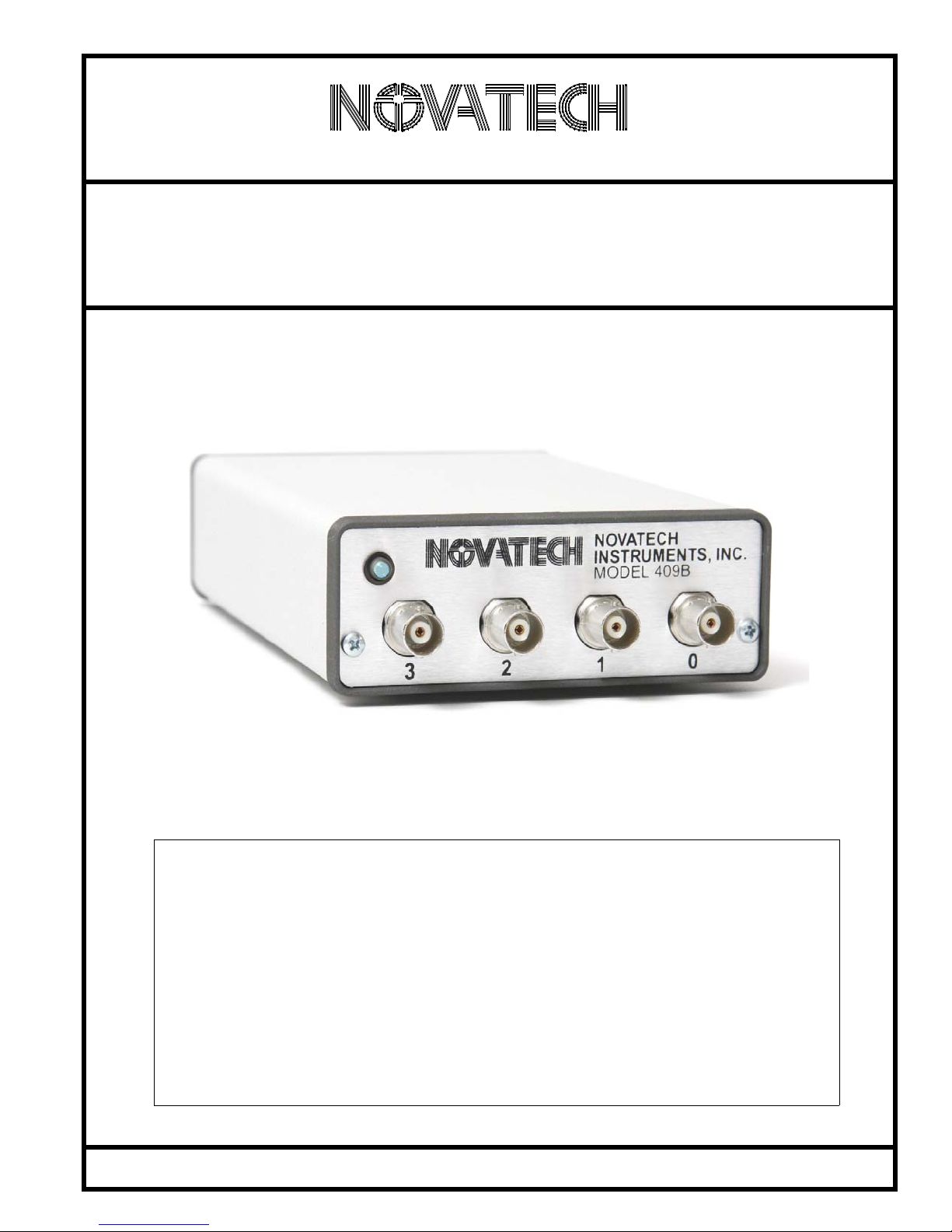
Model 409B 171 MHz 4-Channel Signal Generator
Model 409B
Table of Contents
INSTRUMENTS
Section Page Contents
1.0 . . . . . . . . . . . . . . . . . . . . . . . . . . . . . 2 . . . . . . . . . . . . . . . . . . . . . . . . . Description
2.0 . . . . . . . . . . . . . . . . . . . . . . . . . . . . . 2 . . . . . . . . . . . . . . . . . . . . . . . Specifications
3.0 . . . . . . . . . . . . . . . . . . . . . . . . . . . . . 2 . . . . . . . . . . . . . . . . . Hardware Installation
4.0 . . . . . . . . . . . . . . . . . . . . . . . . . . . . . 5 . . . . . . . . . . . . . . . . . . . . . . . . . . .Operation
5.0 . . . . . . . . . . . . . . . . . . . . . . . . . . . . . 6 . . . . . . . . . . . . . . . . . . Theory of Operation
6.0 . . . . . . . . . . . . . . . . . . . . . . . . . . . . . 8 . . . . . . . . . . . . . . . . . . . . .Performance Test
7.0 . . . . . . . . . . . . . . . . . . . . . . . . . . . . . 9 . . . . . . . . . . . . . . . . . . . . . . . . . .Calibration
8.0 . . . . . . . . . . . . . . . . . . . . . . . . . . . . .10 . . . . . . . . Appendix A: Table Mode Details
9.0 . . . . . . . . . . . . . . . . . . . . . . . . . . . . .12 . . . . . . . . Appendix B: External Reference
--. . . . . . . . . . . . . . . . . . . . . . . . . . . . . . .13 . . . . . . . . . . . . . . . . . . . . . . . . . . . Warranty

NOVATECH INSTRUMENTS 2 409B Manual, 17-Apr-2015
1.0 DESCRIPTION
1.1 The Model 409B is a four-channel Direct Digi-
tal Synthesizer (DDS) in a small table top case with
RS232 serial control. The 409B provides four inde-
pendent, phase-synchronous sine wave (consult fac-
tory for LVCMOS) output signals, which can be set
from 0.0 Hz (DC) to 171 MHz in 0.1 Hz steps when
using the internal VCTCXO clock.
1.2 The 409B can also be used with an External
Clock input. An on-board programmable frequency
multiplier generates the master clock allowing user
configured frequency ranges. The multiplier can be
disabled for direct inputs up to 500 MHz for opti-
mum phase noise performance. When used with the
same external clock source, multiple 409B are phase
synchronous.
1.3 The /R option converts the External Clock input
to a 10.00 MHz reference input. Using the same
topology as our locking programmable oscillator
modules, this options allows locking to and tracking
of an external 10.00 MHz, with no binary round-off
errors. When this option is installed the accuracy
and stability of the output are equal to those of the
reference.
2.0 SPECIFICATIONS
2.1 OUTPUTS
TYPES: Four Sine simultaneously (four independent,
phase-synchronous outputs.)
IMPEDANCE: Sine: 50 Ω; LVCMOS: 50 Ω.
RANGE: 0.0 Hz to 171 MHz in 0.1 Hz steps (Sine out, int.
clock).
SINE AMPLITUDE: approximately 1 Vpp (+4dBm) into
50Ω. Programmable from 0/1024 to 1023/1024 of Full
Scale (10-bits), or by scale factors of 1/2, 1/4, or 1/8.
PHASE: Each channel 14-bits programmable (0.022o).
FLATNESS: ±3dB from 1 kHz to 150 MHz referenced to
amplitude at 35 MHz, full scale.
2.2 LVCMOS AMPLITUDE
Voh >=2.4V and Vol <=0.4V when series terminated. Rise
and fall times <1.5ns. (>1 MHz, <125 MHz) (consult fac-
tory for LVCMOS)
2.3 CONTROL
Output frequencies, amplitudes (10-bits) and phases (14-
bits) are controlled by an RS232 serial port at 19.2kbaud,
or direct connection to the DDS generator. All settings
(except table mode data) can be saved in non-volatile
(EEPROM) memory via the RS232 port.
2.4 ACCURACY AND STABILITY
Accuracy: <±1.5ppm at 10 to 40oC. Stable to an addi-
tional ±1ppm per year, 18 to 28oC. (Internal Clock)
2.5 EXTERNAL CLOCK IN
LEVEL: 0.2 to 0.5 Vrms Sine or Square Wave. 50 Ω.
FREQUENCY: 10 MHz to 125 MHz with multiplier of 4 to
20 enabled. Direct input of 1 MHz to 500 MHz.
/R Option: 10.00 MHz, ±5ppm. Automatically detected.
Internal clock is locked to and tracks this value.
2.6 SPECTRAL PURITY (Typ. 50Ωload, internal
clock, full-scale output)
Phase Noise: <-120dBc, 10kHz offset, 10 MHz out.
Spurious: <-60dBc below 10 MHz (typ. 300MHz span)
<-60dBc below 40 MHz
<-55dBc below 80 MHz
<-50dBc below 160 MHz
Harmonic: <-65dBc below 1 MHz
<-55dBc below 20 MHz
<-45dBc below 80 MHz
<-35dBc below 160 MHz
(channel-channel isolation: <-60dBc)
2.7 TABLE MODE
On-board 4Mb static ram holds up to 32,768 profile
points in table mode allowing a different output in 100 µS
increments.
2.8 POWER REQUIREMENTS
+4.5 to +5.5 VDC <1Amp. AC adapter provided.
2.9 SIZE
39mm H, 107mm W, 172mm L, not including connectors.
2.10 CONNECTORS
BNC for Sine Outputs and EXT CLK IN. DE9 for Serial
Control. 2.5mm center positive power receptacle for +5
volts input. AC-adapter provided.
2.11 OPTIONS
Model 409B-AC adds two rear-panel SMA connectors for
external control of output update and table timing (see
AN002). /R Option converts the External Clock In to a
10.00 MHz external reference input (see Appendix B).

NOVATECH INSTRUMENTS 3 409B Manual, 17-Apr-2015
3.0 HARDWARE INSTALLATION
3.1 Power Connection. The required power of
+5Volts DC is applied through a 2.5mm center-posi-
tive power connector (Switchcraft 712A or equiva-
lent). The Novatech Instruments, Inc. supplied AC-
adapter comes complete with the correct mating
connector.
WARNIN G:
Use of an unregulated source may damage the 409B.
Use only the provided AC-adapter or consult
Novatech Instruments, Inc. for application
assistance if you wish to use another power source.
3.2 The quality of your power supply affects the
performance of the 409B. The supply should be free
of ripple and noise (<50mV). Even though extensive
filtering is used internal to the 409B, a quiet and
well regulated power supply will ensure optimum
performance. The supplied AC-adapter has been
tested for proper operation.
3.3 Installation. To use the 409B, connect your
host computer to the 9-pin female RS232 connector
on the rear panel of the 409B. If you are using a PC,
a 9-pin monitor extension cable used as an RS232
cable will allow direct connection to the 409B with-
out the use of a null modem cable or gender changer.
If you are using a different computer, terminal or
other control source, please note that the data TO
the 409B is on pin 3; the data FROM the 409B is on
pin 2 and the COMMON return is on pin 5. Set your
host to 19.2 kBaud, 8 bits, 1 stop bit, no parity and
no hardware flow control. See Table 2 for Serial
Commands.
3.4 A USB to RS232 adapter cable is available for
use with computers that do not provide a serial port.
Follow the manufacturer’s installation instructions
when using a USB adapter.
3.5 Commands are not case sensitive. There must
be a space after each command except R,CLR,S
and QUE. End with any combination of CR, LF or
CRLF. Illegal commands will result in an error
code being returned per Table 1.
3.6 The “QUE” command returns five hexadecimal
strings reflecting the present state of the 409B. See
page 7 for an explanation of the values that make up
these strings. Note that the frequency settings will be
scaled as discussed below if an external clock is
used.
3.7 The “B” command can cause erroneous opera-
tion and must be used with care. Contact Novatech
Instruments, Inc. for application assistance if you
wish to use this command. Detailed knowledge of
the operation of the Analog Devices AD9959 DDS
generator is required.
NOTE:
The program SOF8 is supplied with the 409B. This
program provides a graphical interface for all the
serial commands, allowing simple control of the
409B.
3.8 Internal Clock. If you plan to use the 409B
internal clock, which is the default setup mode, no
action is required. If the 409B was previously set to
use the external clock, send the serial command “C
i” to reselect the internal clock. If you wish to
maintain this setting, use the save command “S”.
3.9 External Clock. If you are providing your own
clock source, send the serial command “C e”.
Apply your clock to the External Clock Input BNC
on the rear panel. Note that phase noise and stability
Table 1: RS232 Error Codes
Error Code Meaning
OK Good command received
?0 Unrecognized Command
?1 Bad Frequency
?2 Bad AM Command
?3 Input line too long
?4 Bad Phase
?5 Bad Time
?6 Bad Mode
?7 Bad Amp
?8 Bad Constant
?f Bad Byte

NOVATECH INSTRUMENTS 4 409B Manual, 17-Apr-2015
Table 2: Serial Commands
RS232 Command Function
Fn xxx.xxxxxxx Set Frequency of output “n” in MHz to nearest 0.1 Hz. Decimal point required. Set
to 0.00 to turn off a channel. n=0, 1, 2, 3. Maximum setting: 171.1276031 MHz.
Single tone mode.
Pn N Set Phase of output “n”. N is an integer from 0 to 16383. Phase is set to N*360o/
16384 or N*π/8192 radians. Sets the relative phase of the frequency output
depending upon the value of n=0, 1, 2, 3. Single tone mode.
Vn N Set voltage level of output “n”. In default, the amplitude is set to the maximum:
approximately 1Vpp (+4dBm) into 50Ω. N can range from 0 (off) to 1023 (no
decimal point allowed). Voltage level is scaled by N/1023. n=0, 1, 2, 3 to set the
amplitude on frequency 0, 1, 2 or 3. If N >=1024, the scaling is turned off and the
selected output is set to full scale.
E x Serial echo control. x=D for Echo Disable, x=E for Echo Enable
C x Select clock source. x=E for External clock, x=I for Internal Clock. May require
adjustment of Kp and the addition of external filtering of output. (Do not use this
command if the /R option is installed)
RReset. This command resets the 409B. EEPROM data is preserved and, if valid, is
used upon restart. This is the same as cycling power.
CLR Clear. This command clears the EEPROM valid flag and restores all factory
default values.
A x x=E for LVCMOS Enable, x=D for LVCMOS Disable. (consult factory for
LVC M O S)
SSaves current state into EEPROM and sets valid flag. State used as default upon
next power up or reset. Use the “CLR” command to return to default values.
QUE Return present frequency, phase and status. Returns a character string of all inter-
nal settings.
M N Mode command. Mode ‘0’ is single tone on all channels (default). If N=a, then the
phase is automatically cleared during each command; if N=n, then the phase is not
cleared (default). See Section 4.0 for details. See appendix for table mode.
Vs N Set the output Voltage scaling factor. N=1 for full scale, N=2 for one-half scale,
N=4 for one-quarter scale and N=8 for one-eighth scale. All channels are scaled
equally.
Kp aa Set PLL reference multiplier constant. Must be one Hexadecimal byte as two
characters. Legal values are 1 (bypass PLL) and 4 to 20 (01h, 04hto 14h). Values of
Kp times clock frequency must not be between 160MHz and 255MHz (for internal
clock, this disallows 5<=Kp<= 9). (see paragraph 4.12) Not used with /R option.
I x Set the I/O update pulse method. If x=a, then an I/O update is issued at the end of
each serial command (default). If x=m, then a manual I/O update pulse is sent by a
subsequent ‘I p’ command. (see section 4.0 for details)
B aa[bb[cc[dd[ee[ff[gg]]]]]] This Byte command allows each register in the DDS chip to be set. Different
registers require a various number of bytes to be written depending upon the
function. Please consult the manual for details. Note that it is possible to set the
DDS chip into a non-functional mode, requiring a power cycle to recover. All
values are in hexadecimal and no error checking, other than correct format, is
performed.

NOVATECH INSTRUMENTS 5 409B Manual, 17-Apr-2015
are dependent upon your supplied clock. See specifi-
cations for signal levels required and acceptable fre-
quency range. If you wish to maintain this setting,
use the save command “S”.
3.10 The external clock can also be used with Kp=1
for direct connection to the DDS generator. With
Kp=1, the PLL multiplier is disabled. Use this direct
input, up to 500 MHz, for optimum phase noise per-
formance.
NOTE:
When using an external clock, frequency scaling of
the “F” command may be required. Please see
Operation, Section 4, for details. If your unit has the
/R option installed, see Appendix B.
3.11 Signal Outputs. There are four signal outputs
on the 409B labelled 0 to 3 on the front panel BNCs.
These correspond to channels F0 through F3, and
other commands. Simply connect your 50Ωapplica-
tion cable to appropriate output.
3.12 Mounting. An optional 1U rack adapter is
available for mounting up to four 409B into a rack
panel. Please consult factory.
4.0 Operation
4.1 Power on reset. After power is applied, the
409B takes approximately 500ms to initialize. Com-
mands sent during this time will be ignored or may
cause erroneous operation.
4.2 Specifications are met within approximately 15
minutes of power up.
4.3 After the 409B has been installed in the cus-
tomer application system, all that is required for
operation is to send the appropriate serial commands
per Table 2.
4.4 The user host computer software must properly
format the serial commands. Incorrect formatting
will result in an error code being returned. See Table
1 for a list of error codes.
4.5 For maximum interface speed, it is suggested
that Echoing be disabled by the “E d” command.
This will allow the host to send characters at a faster
rate. Note that no flow control is provided. Depend-
ing upon your host, the 409B may not be able to
keep up with serial characters. The 409B will
respond with an “OK” for a correctly received data
command. You will have to verify correct operation
at your host rate.
4.6 A special baud rate command is available if you
wish to set a different baud rate. The value set by
this command is volatile and not saved in EEPROM.
Upon power up, reset or clear, the 409B defaults to
19.2kBaud.
Kb 78 ;9.6kBaud
Kb 3c ;19.2kBaud
Kb 1e ;38.4kBaud
Kb 14 ;57.6kBaud
Kb 0a ;115.2kBaud
4.7 If you are using an external clock, the value sent
to the 409B in the “Fn” command must be scaled.
The output frequency of the 409B when used with
an external clock is given by:
Fout = (Fcommand)*(Kpe*Fext clk)/(Kpi*Fint clk)
Where Kpe is the value of Kp set by the
customer, and Kpi is the internal default Kp
(0x0f).
4.8 The nominal Internal Clock has a value of
28,633,115.306666666 Hz (232/150). Best perfor-
mance is obtained when the External Clock input
times the Reference PLL multiplier (Kp) is close to
the default value (429.4967296 MHz, max: 500
MHz), as the on-board filters are optimized for that
range.
4.9 For an example of scaling, suppose an external
clock of 10.000 MHz is used and an output of 1.544
MHz is desired (Kp=15):
Fcommand = (1.544)*(15*28,633,115.306666667)/
(15*10,000,000)
= 4.4209530
4.10 The command then sent to the 409B for the
1.544 MHz output, with a 10 MHz external clock,
will be (assuming Kp is unchanged):

NOVATECH INSTRUMENTS 6 409B Manual, 17-Apr-2015
Fn 4.4209530
where ‘n’ is your selected channel
NOTE:
You must account for your clock frequency error and
calculation roundoff when using an external clock.
Some hand calculators may not have enough digits
to match the resolution of the 409B. See Appendix B
if your unit has the /R option installed.
4.11 Beginning with Software Revision 2.1, it is
possible to control the internal range bit on the DDS
ASIC.
4.12 For normal operation the Kp command is
unmodified. However, if it is desired that the clock
multiplier gain bit be set HIGH (for Kp*[Ext Clk
Freq] from 255 and 500 MHz), add hexadecimal
0x80 to the Kp value to be set. For the bit to be
forced LOW (100 to 160 MHz), add hexadecimal
0x40 to the Kp value to be set.
4.13 Since the resolution of the 409B is 32-bits, the
typical fractional frequency error (∆f/f) for output
frequencies in the MHz range will be less than
0.1ppm, even when exact values are not possible.
NOTE:
The “B”command can be used to test AD9959 DDS
chip programming as it allows access to all internal
registers. While not a real-time simulation, each
“B”command functions as an input by putting a
data byte directly into the AD9959 via an SPI port,
and then pulses the IOUD line. This is the similar to
a procedure that a customer control circuit might
perform. Consult the Analog Devices AD9959 data
sheet for detailed information.
4.14 Phase relationships are maintained by appro-
priate use of the “M” and “I” commands. The “M”
command has special modes “M a” and “M n”.
“M a” means automatically clear phase at the end
of each command. This will clear the phase register
each time any command is performed. This is
important when all outputs must be phase aligned.
However, it will cause a phase jump in the output.
4.15 The “M n” command turns off the automatic
clearing of the phase register. This is the default
mode. In this mode, the phase register is left intact
when a command is performed. Use this mode if you
want frequency changes to remain phase synchro-
nous, with no phase discontinuities.
4.16 Further control of phase relationships and tim-
ing of command execution can be exercised by
using the “I m”, “I a” and “I p” commands.
The default mode is “I a” in which a command is
parsed and executed immediately following the end
of the serial input sequence. In the “I m” mode, an
update pulse will not be sent to the DDS chip until
an “I p” command is sent. This is useful when it is
important to change all the outputs to new values
simultaneously.
4.17 For applications which require precise ampli-
tude matching between the channels, the recom-
mended method is to use the “Vn N” command to
adjust the channels to match the other. This com-
mand provides 10-bits of adjustment range.
5.0 Theory of Operation
5.1 Please refer to the simplified System Block Dia-
gram in Figure 3 for the following discussion.
5.2 At every cycle of the 409B master clock, the 32-
bit DDS integrated circuit increments the phase of
an internal register by a value determined by the fre-
quency setting loaded into the on-chip registers.
This digital phase value is converted on-chip to a
sinusoidal amplitude level and delivered to on-chip
10-bit digital-to-analog converters. The analog sig-
nals from these converters are filtered by differential
7th-order elliptical low pass filters, amplified and
sent to the BNC receptacles.
Typical ∆f/f for External Clock of 10.0MHz
Kp
Desired
Fout Command ∆f/f
15 1.544MHz Fn 4.4209530 2.19x10⁻⁸
20 1.544MHz Fn 3.3157148 1.43x10⁻⁸
15 2.048MHz Fn 5.8640620 1.45x10⁻⁸
20 2.048MHz Fn 4.3980465 2.02x10⁻⁸

NOVATECH INSTRUMENTS 7 409B Manual, 17-Apr-2015
O
WER
LOGIC
32-Bit
DDS,
LP Filter,x4 AMP,x4 Sine
OU
T
Buffer,x4 LVCMO
OUT
POWER
FILTERS &
+5V
-5V
Master
Clock
EXT
CLK
IN
CLK SEL
Figure 3.
Simplified System Block Diagram
409B
S
232 µCSystem Control
+1.8V
REGULATOR
Volta
g
Contr
o
AD9959,
V
+3.3V
4 channels
“Que” command output (all values are hexadecimal) values:
05F5E100 0000 03ff 0000 00000000 00000000 000301
05F5E100 1000 03ff 0000 00000000 00000000 000301
05F5E100 0000 03ff 0000 00000000 00000000 000301
05F5E100 1000 03ff 0000 00000000 00000000 000301
80 BC0000 0000 6102 21
Description:
Line 1: “05F5E100”, frequency in 0.1Hz steps per LSB; “0000”, phase setting; “03ff”, amplitude setting
(default is scaling off, so output is full-scale); “0000”, linear ramp rate; “00000000”, rising delta frequency;
“00000000”, falling delta frequency, “000301”, channel function register.
The last line gives the status of AD9959 registers and internal software registers: “80”, channel select register
(CSR); “BC0000”, function register 1 (FR1); “0000”, function register 2 (FR2); “6102”, internal µC control
registers; “21”, software revision as x.y, Rev 2.1 in this example. Consult the Analog Devices AD9959 data
sheet for meaning of registers. Each line is terminated by a carriage return/line feed (CRLF) pair.

NOVATECH INSTRUMENTS 8 409B Manual, 17-Apr-2015
5.3 The frequency generated by the DDS IC is
determined by the 32-bit frequency word loaded into
the frequency register on the 409B. The output fre-
quency is given by:
Fout = Fsetting*Kp*Fclock/232 Hz
Where: Fclock = 28,633,115.306666667 Hz (int.)
Fsetting = Binary value in DDS IC.
(Fsetting ranges from 0 to 231-1)
Kp = PLL Multiplier (1 or 4 to 20)
This reduces to:
Fout = Fsetting MHz
for the internal (default) clock and the default PLL
Multiplier (Kp=15) settings.
5.4 Since the DDS IC is a sampled data system, the
output frequency is limited to a maximum of 1/2 the
master clock frequency (Fsetting <= 231-1). While it
is possible to generate an output near 50% of the
clock, the distortion may be unacceptable. There-
fore, the output is limited to approximately 40% of
the system clock and steep output filters are pro-
vided on board: in this case 7th-order elliptical low
pass filters.
5.5 If you are using an external clock and a Kp
which give a clock substantially lower than the
429.497 MHz default internal clock, you may need
to filter the Outputs to obtain acceptable distortion
for your application. For best performance, set the
corner frequency at 40% or less of your external
clock frequency times Kp. The lower your filter as a
percentage of your clock frequency, the lower the
distortion.
5.6 For example, if you are using a 10 MHz external
clock, with the default reference multiplier (Kp) of
15, then the internal clock is 150 MHz. An optimal
filter for this frequency would then be approxi-
mately 60 MHz (40% of 150 MHz).
6.0 PERFORMANCE TEST
6.1 Install the 409B as directed in the Serial Opera-
tion part of Section 3. Connect your host controller
and operate the 409B per Section 4. The test limits
assume a stable environment of 18-28oC.
NOTE:
Allow the 409B to warm up for at least 15 minutes
before performing any measurements. For best
results, the 409B should be verified in its installed
environment.
6.2 See Table 3 for a list of recommended test
equipment to perform the following measurements.
6.3 Verify Frequency Accuracy. To verify the fre-
quency of the 409B, set the output sequentially to
each value in Table 4. Connect the recommended
frequency counter set to 50Ωtermination and 1Hz
resolution. Verify the limits show in Table 4. Test all
channels to verify functionality of all outputs. If you
do not use an external reference for the frequency
counter, be sure to add the error of your counter to
the tolerance. (LSD = Least Significant Digit on
counter).
Table 3: Recommended Test Equipment
Item
Minimum
Specification Recommended
Oscilloscope 300 MHz,
50Ω
Tektronix
TDS3032B
50ΩTermination 50Ω, ±1% Tektronix
011-0049-01
Frequency
Counter
180 MHz HP53132A
Counter Time
Base
10 MHz,
<±0.1ppm
Novatech
Instruments
Model 2960AR
External Clock 400 MHz Novatech
Instruments
Model 440A
Table 4: Frequency Test Points
Frequency Tolerance
100 kHz ±0.15 Hz ±1 LSD
1 MHz ±1.5 Hz ±1 LSD
10 MHz ±15 Hz ±1 LSD

NOVATECH INSTRUMENTS 9 409B Manual, 17-Apr-2015
6.4 Sine Out Amplitude Verification. Set the fre-
quency of the 409B to 10 MHz. Connect the 409B to
the oscilloscope set for 50Ωtermination. Set the
oscilloscope to measure to amplitude using at least
16 averages. Verify a reading of 1Vpp ±0.25Vpp.
Repeat for the other outputs.
6.5 Level Command Test. Leave the output fre-
quency set to 10 MHz. Send the commands “Vn
512” to each channel, where “n” is your channel
number being tested. Verify that the amplitude on
each channel decreases by one-half. Send the “R”
command to reset the levels before performing the
next tests.
6.6 Output Flatness Verification. Verify that the
outputs are flat with frequency by performing the
following test: Connect the 409B to the oscilloscope
set for 50Ωtermination. Use the same settings as
Sine Out Amplitude Verification. Note the voltage
reading.
6.7 Set the 409B to the values of Table 4. Verify that
the oscilloscope amplitude reading remains within
±3dB (x1.414 to x0.707) of the value noted in the
previous paragraph. (limit upper frequency to150
MHz)
6.8 Repeat the output flatness verification test for
each output.
6.9 External Clock Input Verification. Set the fre-
quency output to 10.000 MHz by sending the com-
mand “F0 10.7374182” (scaled per section
4.0). Connect a 400 MHz external clock source via a
short coaxial cable to the external clock BNC on the
rear panel. Send the command “Kp 01”. Send the
command “C e” to select the external clock input.
6.10 Verify an output of 10.0000000 MHz, ±1 Hz.
You must account for any frequency errors in your
external clock source.
6.11 Return the 409B to normal operation and
default values by sending the “CLR” command.
6.12 This concludes the verification test of the
409B.
7.0 CALIBRATION
7.1 The 409B has two adjustable components: Y2,
frequency, and R22, output amplitude. Calibration
should be performed only if the 409B fails the per-
formance test or if the unit has been repaired. Rou-
tine adjustments are not recommended nor generally
required. This procedure assumes that the 409B has
failed the performance test or has been repaired.
WARNING:
Calibration of the Model 409B requires that the case
be opened. Calibration should be performed only by
qualified personnel. The internal components are
static sensitive.
7.2 Access to the adjustments is provided by remov-
ing the rear panel fasteners. Remove the two phillips
head screws on the rear panel, the power receptacle
nut, and the two jack-screws holding the RS232 con-
nector. Tip the rear panel away from the instrument
and slide the top cover off. Be careful not to unduly
flex the connecting wires.
7.3 The adjustments shown are set to 1/2 the speci-
fication values.
NOTE:
Allow the 409B to warm up for at least 15 minutes
before performing any adjustments. For optimum
performance the 409B should be calibrated in an
environment similar to its installation.
NOTE:
If your unit has the /R option installed, the oscillator
adjustment is the same, except the location has
moved to the adapter board.
7.4 Frequency Adjust, Y2. Set the output of the
409B to 10.0000000 MHz using the command “F0
10.0000000”. Connect output of channel 0 to
your frequency counter set for 50 Ωtermination.
30 MHz ±45 Hz ±1 LSD
50 MHz ±75 Hz ±1 LSD
100 MHz ±150 Hz ±1 LSD
170 MHz ±255 Hz ±1 LSD
Table 4: Frequency Test Points
Frequency Tolerance

NOVATECH INSTRUMENTS 10 409B Manual, 17-Apr-2015
Adjust Y2 using a non-metallic adjustment tool for
10.000000 MHz, ±7.5 Hz.
NOTE:
If your unit has the /R option installed, the access to
R22 is blocked by the module. Remove the two
screws securing the module and carefully reposition
the module to allow access to R22.
7.5 Amplitude Adjust, R22. Connect the output of
channel 0 to the oscilloscope set to measure ampli-
tude, with a minimum of 16 averages. Set for 50 Ω
termination. Set the output to 35 MHz by sending
the command “F0 35.0000000”. Adjust R22
for 1.00 Vpp ±0.075 Vpp. This completes the cali-
bration of the Model 409B.

NOVATECH INSTRUMENTS 11 409B Manual, 17-Apr-2015
8.0 Appendix A. Table Mode Details.
8.1 The Model 409B contains on-board static RAM
capable of storing up to 32,768 profile points. Each
point contains phase, frequency, amplitude and
dwell time information. The on-board microcom-
puter reads this RAM and programs the DDS ASIC
per the profile point data. The profile can be set to
loop continuously or to hold at the last point, until
interrupted by a subsequent command.
NOTE:
Only Channels 0 and 1 can be set with the table
mode.
8.2 The table mode is toggled on and off by an ‘M
t’ command from the serial port and executes cus-
tomer provided profile points. ‘M 0’ always turns
off the table and returns to single tone mode. The
409B starts execution of the profile immediately
upon a receipt of ‘M t’ following an ‘M 0’.
8.3 The command sequence (bold) is of this form
(comments after the ‘;’ are not sent to the 409B, but
are here for explanation purposes):
M 0
;turns off running table mode
t0 0000 aabbccdd,eeff,gghh,ii
;F0 profile point 0, on output 0
t1 0000 aabbccdd,eeff,gghh,ii
;F1 profile point 0, on output 1
t0 0001 aabbccdd,eeff,gghh,ii
;F0 profile point 1
t1 0001 aabbccdd,eeff,gghh,ii
;F1 profile point 1
...
t0 3fff aabbccdd,eeff,gghh,ii
;F0 profile point 0x3fff
t1 3fff aabbccdd,eeff,gghh,ii
;F1 profile point 0x3fff
M t
;begin execution of table
;‘0000’ two byte RAM address, T0 and T1 must
be paired with same address
;‘aabbccdd’ four bytes frequency, hexadecimal,
MSB first, 4 bytes. 0.1Hz resolution on LSB
;‘eeff’ phase offset, hexadecimal, MSB first,
only 14-bits active, top two bits are ignored
;‘gghh’ amplitude scale, MSB first, only 10-bits
active. Amplitude is scaled per above.
;‘ii’ dwell time, MSB first, in increments of
100µs. 0x00=loop back to start, 0xff=hold present
setting. Each T0-T1 pair must have the same dwell.
8.4 The ‘,’ (comma) in each record is used as a
delimiter and must be included as shown. The inputs
are not case sensitive. Subsequent ‘M t’ com-
mands will toggle the execution of the table on and
off. Upon execution of the table, the output will
always begin with address 0000 and progress until it
encounters an 0xff or 0x00 in a dwell position. The
last record in a table mode will be executed for
100µs if the dwell is set to 00.
NOTE:
Each record must be terminated with an 0x00 or 0xff
in the dwell position to indicate the end of your data.
8.5 The current values stored in RAM can be read
back by the “Dn aaaa” command. N=0 or 1 and
“aaaa” is the address.
8.6 The RAM table is backed-up by a “supercap”
for a minimum of 10 minutes. This allows for short
power interrupts without losing the table informa-
tion. (Consult factory for battery backup options).
8.7 Other Modes. The 409B can be programmed
by using the “B” command to perform many other
outputs. The “B” command can be used to gain con-
trol over the on-board AD9959 DDS ASIC. Refer to
the Analog Device data sheet for detailed informa-
tion when using the “B” command.
8.8 See AN003 for the Model 409B/01 which
includes a variable pulse width (variable symmetry)
output option.

NOVATECH INSTRUMENTS 12 409B Manual, 17-Apr-2015
9.0 Appendix B. External Reference
Option.
9.1 The /R option converts the external clock input
to a 10.00 MHz reference input (consult factory for
5.00 MHz). This option provides locking and track-
ing circuitry to generate an exact binary clock
needed to allow even output steps.
9.2 The external clock input on the 409B series is
changed to accept 10.00 MHz. A reference input
signal is automatically detected and, if within a lock
range of approximately ±5ppm, it is locked to and
tracked by the narrow-band phase lock loop.
9.3 If an input signal is not detected, the unit will
default to the internal free-running oscillator and
perform identically to a 409B without the /R option.
9.4 The front panel LED will display four condi-
tions:
Steady Green: unit is locked to a stable refer-
ence, or is using the free running clock.
Blinking Green: unit is stabilizing to a free run-
ning condition. This occurs upon power-
up or if the reference is removed.
Steady Red: unit detects an external input, but
cannot lock to it.
Blinking Red: unit has detected a change in the
reference and is attempting to lock. This
will occur if a reference is applied to a
unit that has been free running.
9.5 When changing the reference mode, the phase
lock loop may take several minutes to stabilize to
the final resolution of the 409B. Changing from a
blinking LED to a stable LED indicates that the pro-
cess is completing, but you should verify the out-
puts.
9.6 The /R option diverts the external clock line so
the “C E” command is no longer valid. The “Kp”
command should not be used. If either command is
used with the /R option, you will get unpredictable
behavior.

NOVATECH INSTRUMENTS 13 409B Manual, 17-Apr-2015
WARRANTY
NOVATECH INSTRUMENTS warrants that all instruments it manufactures are free from defects in
material and workmanship and agrees to replace or repair any instrument found defective during a period
of one year from date of shipment to original purchaser.
This warranty is limited to replacing or repairing defective instruments that have been returned by
purchaser, at the purchaser's expense, to NOVATECH INSTRUMENTS and that have not been subjected
to misuse, neglect, improper installation, repair alteration or accident. NOVATECH INSTRUMENTS
shall have the sole right to final determination regarding the existence and cause of a defect.
This warranty is in lieu of any other warranty, either expressed or implied, including but not limited to
any warranty of merchantability or fitness for a particular purpose. In no event shall seller be liable for
collateral or consequential damages. Some states do not allow limitations or exclusion of consequential
damages so this limitation may not apply to you.
All instruments manufactured by NOVATECH INSTRUMENTS should be inspected as soon as they are
received by the purchaser. If an instrument is damaged in shipment the purchaser should immediately file
a claim with the transportation company. Any instrument returned to NOVATECH INSTRUMENTS
should be shipped in its original shipping container or other rigid container and supported with adequate
shock absorbing material.
This warranty constitutes the full understanding between NOVATECH INSTRUMENTS and the
purchaser and no agreement extending or modifying it will be binding on NOVATECH INSTRUMENTS
unless made in writing and signed by an authorized official of NOVATECH INSTRUMENTS.
NOVATECH INSTRUMENTS
4210 198th St SW Suite 204
Lynnwood, Washington 98036
United States of America
FAX: 425.361.1550
TEL: 206.301.8986
http://www.novatechsales.com/
Copyright 2007-2015 Novatech Instruments
Table of contents


