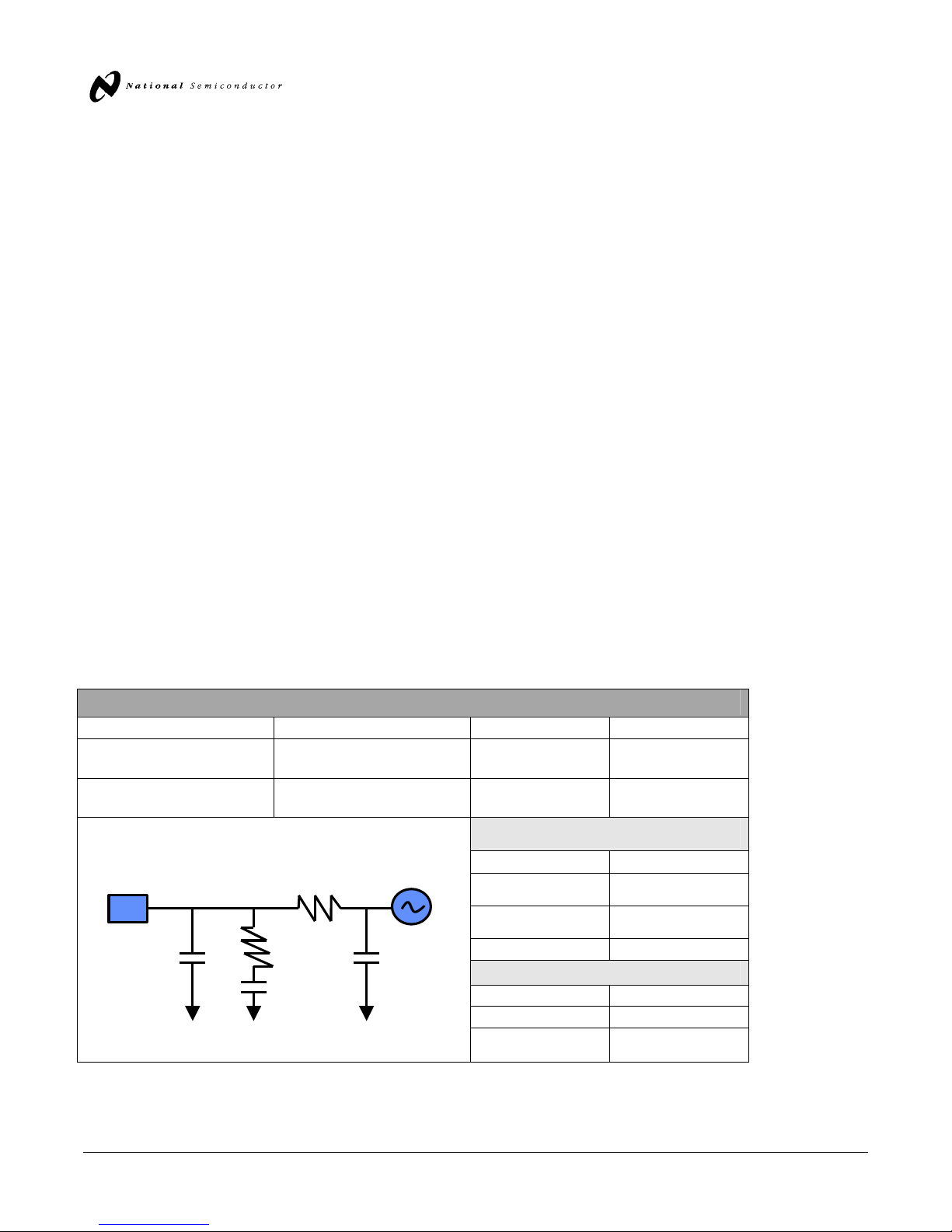
LMX2306TM EVALUATION BOARD INSTRUCTIONS
Appendix C - LMX2306TM Evaluation Board - Bill of Materials
Item
# QTY Part Number Description Reference
Designators Preferred Vendor
0 7 N/A Open, No component CX, C3, RX, R18,
J1, J3, J4 N/A
1 4 C0603C103J4RAC CAP, 0.01 µF, Ceramic, 5%,
X7R, 0603 C7, C8, C11, C13 Kemet
2 4 C1206C105J8RAC CAP, 1.0 µF, Ceramic, 5%,
X7R, 1206 C10, C14, C15 Kemet
3 4 C0603C101J5GAC CAP, 100 pF, Ceramic, 5%,
NP0, 0603 C4, C5, C6, C16 Kemet
4 1 C0805C102J5GAC CAP, 1000 pF, Ceramic,
5%, NP0, 0805 C9 Kemet
5 1 C0603C681J3GAC CAP, 680 pF, Ceramic, 5%,
NP0, 0603 C1 Kemet
6 1 C0603C562J3RAC CAP, 5600 pF, Ceramic,
5%, X7R, 0603 C2 Kemet
7 1 CRCW0603000ZRT1
RES, 0 Ω, 0603 R3 Vishay
8 1 CRCW0603100JRT1
RES, 10 Ω, 5%, 0603 R4 Vishay
9 4 CRCW0603103JRT1
RES, 10.0 K Ω, 5%, 0603 R1, R6, R7, R8 Vishay
10 2 CRCW0603180JRT1
RES, 18 Ω, 5%, 0603 R12, R13 Vishay
11 4 CRCW0603223JRT1
RES, 22 K Ω, 5%, 0603 R9, R10, R11, R17 Vishay
12 1 CRCW0603510JRT1
RES, 51 Ω, 5%, 0603 R5 Vishay
13 2 CRCW0603270JRT1
RES, 27 Ω, 5%, 0603 R15, R16 Vishay
14 1 CRCW0603390JRT1
RES, 39 Ω, 5%, 0603 R14 Vishay
15 1 CRCW0603153JRT1
RES, 15 K Ω, 5%, 0603 R2 Vishay
16 1 HTSM3203-4G2 HEADER, 4 Pin JP2 Comm Con
Connectors
17 1 HTSM3203-6G2 HEADER, 6 Pin JP1 Comm Con
Connectors
18 1 LMX2306TM IC, PLL U1 National
Semiconductor
19 1 LMX2306TMEBPCB PCB National
Semiconductor
20 3 5762SF CONNECTOR, SMA, 50 ΩJ2, J7, J8 CDI
21 2 CCIJ255G SHUNT, Single, .100"
Center, Closed Top Comm Con
Connectors
22 1 LVCO 4279U VCO U2 VARIL
23 1 LMXOGTSP FRAME, 2" x 1.5" Lux
Manufacturing
24 4 OF12SHCA SCREW, 0-80x1/8 Orlander Inc
25 6 2C18PPMZZ SCREW, 2-56x3/16, Philips,
pan-head Orlander Inc
810-27-2003