NXP Semiconductors AFD4400-RDB User manual

1 Introduction
The AFD4400 reference design board (AFD4400-RDB) is a
cost-effective, high-performance system comprised of a
printed circuit board (PCB) assembly and a board support
package (BSP) software featuring the AFD4400 processor.
2 Related documentation
The table below lists the documents that may be available only
under a non-disclosure agreement (NDA). To request access to
these documents, contact your local field applications engineer
or sales representative.
Freescale Semiconductor Document Number: AFD4400-RDBQS
Quick Start Rev. 0, 07/2015
AFD4400 Reference Design Board
Quick Start
© 2015 Freescale Semiconductor, Inc.
Contents
1 Introduction.............................. .............................. 1
2 Related documentation............................................1
3 Chassis overview....................... ............................. 2
4 Board interface.......................... ..............................4
5 Initial board start up........................ ........................5
6 Preparing and starting up board.......... ....................6
7 Re-programming NOR flash................................... 7
8 Booting Linux........................... ..............................9
9 Configuring ADI transceiver cards.... ...................10
10 Flash image layout....................... .........................11
11 Default switch settings..........................................12
12 Revision history.................................................... 14
Downloaded from Arrow.com.

Table 1. Related documentation
Document name Description
AFD4400 Digital Front End Processor Electrical
Specifications (document AFD4400EC)
This document contains the specific data regarding the bus timing,
signal behavior, thermal characteristics, and other design
considerations.
AFD4400 Digital Front End Processor Reference
Manual (document AFD4400RM)
This document describes the functionality of the AFD4400 processor
including the specifications, block diagram, registers, connectors, and
interfaces.
Airfast Digital AFD4400-RDB Reference Manual
(document AFD4400-RDBRM)
This document describes the hardware features of the AFD4400-
RDB including the specifications, block diagram, connectors,
interfaces, and hardware straps. It also lists the settings and physical
connections required to boot the board.
AFD4400 RDB Schematic (document SPF-28466) AFD4400-RDB schematic document.
3 Chassis overview
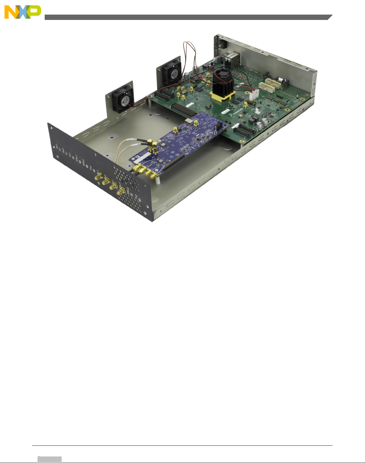
This section shows the front and interior view of the AFD4400-RDB mounted in the chassis.
The below listed figures show the AFD4400-RDB chassis front panel and interior view.
Figure 1. AFD4400-RDB chassis front panel
Chassis overview
AFD4400 Reference Design Board Quick Start, Rev. 0, 07/2015
2 Freescale Semiconductor, Inc.
Downloaded from Arrow.com.Downloaded from Arrow.com.

Figure 2. AFD4400-RDB chassis interior view
NOTE
The ADI card(s) availability in your AFD4400-RDB system depends on the variant you
purchased.
Chassis overview
AFD4400 Reference Design Board Quick Start, Rev. 0, 07/2015
Freescale Semiconductor, Inc. 3
Downloaded from Arrow.com.Downloaded from Arrow.com.Downloaded from Arrow.com.

4 Board interface
This section lists the figures displaying the top and bottom view of the board with the available interfaces.
Power good LED
(Green)
Power connector
(24 V)
Ethernet connector
(Top - SGMII1)
(Bottom - SGMII2) Reset
button
USB connector
(UART4)
Reset LED
(Red)
Universal
reset button
RS485
(UART2)
RS485
(UART1)
ARM RVI connector
VSPA CW connector
Status LEDs
DIP switches
1588 connector
PA3 connector
PA4 connector
FMC2 connector
FMC1 connector
PA1 connector
PA2 connector
Figure 3. AFD4400-RDB top view
Board interface
AFD4400 Reference Design Board Quick Start, Rev. 0, 07/2015
4 Freescale Semiconductor, Inc.
Downloaded from Arrow.com.Downloaded from Arrow.com.Downloaded from Arrow.com.Downloaded from Arrow.com.

Mount area for trace
adapter card CPRI1
REC
CPRI SFP+ cage
CPRI1
RE
CPRI2
REC CPRI2
RE
Figure 4. AFD4400-RDB bottom view
5 Initial board start up
You need to perform an initial board start up to ensure that the board power supplies and the processor is coming out of the
reset state successfully using the default DIP switch settings. To do this, follow the steps listed below:
1. Ensure that the power supply is not connected to your board.
2. Ensure that your board is configured with the default DIP switch settings. For information about the default DIP switch
settings, see Section 11, "Default switch settings".
NOTE
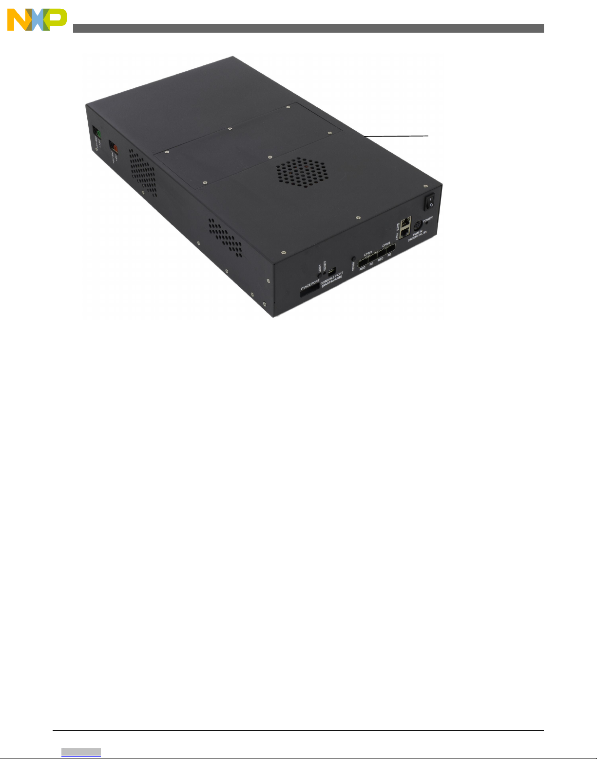
To verify the default DIP switch settings on your board, you need to open the top
cover of the chassis. The figure below shows the top view of the AFD4400-RDB
mounted in chassis.
Initial board start up
AFD4400 Reference Design Board Quick Start, Rev. 0, 07/2015
Freescale Semiconductor, Inc. 5
Downloaded from Arrow.com.Downloaded from Arrow.com.Downloaded from Arrow.com.Downloaded from Arrow.com.Downloaded from Arrow.com.
Top cover
Figure 5. Chassis top view
3. Attach a universal serial bus (USB) cable to the AFD4400-RDB CONSOLE PORT micro-USB port on the chassis
front panel and the host computer.
4. Connect the DC power adapter available in your kit to the PWR IN power connector port on the chassis.
5. Plug the power adapter to your wall outlet.
6. Turn on the power switch on the chassis.
7. Check for the completion of the power-on-reset (PRESET) sequence indicated by the LEDs. The LEDs follow the
sequence listed below:
a. The RESET LED on the chassis and the LEDs D14 to D18 on the board display a steady green light.
b. The LED D19 on the RDB flashes red and turns off, indicating that the AFD4400 processor has exited the reset
state and it is now in a ready state.
c. The FAULT LEDs D7, D12, and D13 stays in the off state, indicating that the system is initiated without any
fault.
8. Turn off the power switch.
NOTE
For more information about the DIP switches and the LEDs available on the
AFD4400-RDB, see the Airfast Digital AFD4400-RDB Reference Manual
(document AFD4400-RDBRM).
6 Preparing and starting up board
To prepare and start up your AFD4400-RDB system, follow the steps listed below:
NOTE
Before you start preparing the board, you must follow the steps listed in the Section 5,
"Initial board start up".
Preparing and starting up board
AFD4400 Reference Design Board Quick Start, Rev. 0, 07/2015
6 Freescale Semiconductor, Inc.
Downloaded from Arrow.com.Downloaded from Arrow.com.Downloaded from Arrow.com.Downloaded from Arrow.com.Downloaded from Arrow.com.Downloaded from Arrow.com.

1. Ensure that the power switch on the chassis is turned off.
2. Install the enhanced small form-factor pluggable (SFP+) optical transceivers as per your application scenario.
NOTE
The FTLF8526P3BNL and FTLX8573D3BTL SFP+ transceivers from Finisar®
are recommended. For more information, see the Airfast Digital AFD4400-RDB
Reference Manual (document AFD4400-RDBRM).
3. Connect the Ethernet cable from the switch/LAN port to the registered jack (RJ45) ETH1 port on the chassis.
4. Plug the power adapter to the wall outlet.
5. Turn on the power switch to boot the board.
The system auto boots and shows the universal boot loader (U-Boot) console and the following message appears on the
screen:
U-Boot 2013.04.Freescale_D4400_v2.4-00009-g981ca73 (Jan 02 2015 - 21:36:36)
CPU:Freescale D4400 prev-0x5d, srev-0x10 at 614 MHz
Reset cause: 0x40000001
DDR Clock: 491MHz
ARM Clock: 614MHz
VSPA Clock: 614MHz
DRAM: 768 MB
Board: D4400-RDB, Rev C
VID: 00 -> 1.0500 Volts
Flash: 256 MB
In: serial
Out: serial
Err: serial
Net: SGMII: eTSEC1 [PRIME], eTSEC2
Hit any key to stop autoboot: 5 4 0
D4400-RDB U-Boot =>
D4400-RDB U-Boot =>
7 Re-programming NOR flash
To re-program the NOR flash, follow the steps listed below:
1. Prepare the board. For the instructions, see Section 6, "Preparing and starting up board".
2. Configure and test the trivial file transfer protocol (TFTP) server using the steps listed below:
a. Ensure that the TFTP server is running.
b. Select the directory where you have saved the BSP release files.
c. Set the serverip variable to the server interface internet protocol (IP) address of the TFTP server application
running on the host PC and save the setting as listed below.
D4400-RDB U-Boot => setenv serverip 10.69.12.25
D4400-RDB U-Boot => saveenv
Saving Environment to Flash...
. done
Un-Protected 1 sectors
. done
Un-Protected 1 sectors
Erasing Flash...
. done
Erased 1 sectors
Writing to Flash... done
. done
Protected 1 sectors
. done
Protected 1 sectors
D4400-RDB U-Boot =>
Re-programming NOR flash
AFD4400 Reference Design Board Quick Start, Rev. 0, 07/2015
Freescale Semiconductor, Inc. 7
Downloaded from Arrow.com.Downloaded from Arrow.com.Downloaded from Arrow.com.Downloaded from Arrow.com.Downloaded from Arrow.com.Downloaded from Arrow.com.Downloaded from Arrow.com.

d. Ensure that the ipaddr (RDB IP address) variable is not in use on your network.
e. Match the netmask variable with the netmask needed for your network.
f. Match the gatewayip (gateway IP address) variable with the gateway on your network and specify the path to
your TFTP server.
NOTE
If you are using a DHCP server, use the dhcp command instead of steps d, e,
and fto obtain the network configuration from the DHCP server.
g. Ping the server to verify the network connectivity using the command listed below at the U-Boot console.
=>run test_tftp
The following output appears on the console:
eTSEC1 Waiting for PHY auto negotiation to complete....done
Speed: 100, full duplex
Using eTSEC1 device
ARP Retry count exceeded; starting again
eTSEC2 Waiting for PHY auto negotiation to complete......... TIMEOUT !
eTSEC2: No link.
Speed: 100, full duplex
Using eTSEC1 device
host 10.69.12.25 is alive
D4400-RDB U-Boot =>
3. Load the U-Boot images using the steps listed below:
a. Download and flash the secondary U-Boot image using the command listed below.
D4400-RDB U-Boot => run get_uboot2
The following output appears on the console:
Speed: 100, full duplex
Using eTSEC1 device
TFTP from server 10.69.12.25; our IP address is 10.69.3.242; sending through
gateway 10.69.3.254
Filename 'u-boot-sha256.d4400'.
Load address: 0x90002000
Loading: ##################
811.5 KB/s
done
Bytes transferred = 259544 (3f5d8 hex)
Un-Protect Flash Sectors 6-9 in Bank # 1
.... done
Erase Flash Sectors 6-9 in Bank # 1
.... done
Copy to Flash... done
Protect Flash Sectors 6-9 in Bank # 1
.... done
D4400-RDB U-Boot =>
WARNING
Do not continue until the previous step is successfully completed, otherwise,
you will risk erasing the primary U-Boot image.
b. When the secondary U-Boot image is successfully loaded, reflash the primary U-Boot image using the command
listed below.
D4400-RDB U-Boot => run get_uboot1
c. Reboot the system.
The U-Boot prompt appears.
4. Load the kernel FIT images using the steps listed below.
Re-programming NOR flash
AFD4400 Reference Design Board Quick Start, Rev. 0, 07/2015
8 Freescale Semiconductor, Inc.
Downloaded from Arrow.com.Downloaded from Arrow.com.Downloaded from Arrow.com.Downloaded from Arrow.com.Downloaded from Arrow.com.Downloaded from Arrow.com.Downloaded from Arrow.com.Downloaded from Arrow.com.
a. Download and flash the primary kernel image using the following command:
D4400-RDB U-Boot => run get_fit1
The following output appears on the screen:
Speed: 100, full duplex
Using eTSEC1 device
TFTP from server 10.69.12.25; our IP address is 10.69.3.242; sending through
gateway 10.69.3.254
Filename 'kernel_fit.itb'.
Load address: 0xb0000000
Loading:
#################################################################
#################################################################
#################################################################
#################################################################
1.1 MB/s
done
Bytes transferred = 26197116 (18fbc7c hex)
Un-Protect Flash Sectors 10-512 in Bank # 1
....................................................................................
..............
....................................................................................
..............
....................................................................................
..............
.........done
Erase Flash Sectors 10-512 in Bank # 1
....................................................................................
..............
....................................................................................
..............
....................................................................................
..............
.........done
Copy to Flash... done
Protect Flash Sectors 10-512 in Bank # 1
....................................................................................
..............
....................................................................................
..............
.........done
b. Similarly, flash the secondary kernel image using the command listed below.
D4400-RDB U-Boot => run get_fit2
You have successfully re-programmed the NOR flash on your board.
8 Booting Linux
To boot the Linux operating system on the AFD4400-RDB, follow these steps:
1. Run the bootcmd environment variable at the U-Boot console using any of the following methods:
•Run the first FIT image from the onboard NOR flash using the command listed below.
run bootcmd_nor
• Download and run the FIT image from the TFTP server using the command listed below.
Booting Linux
AFD4400 Reference Design Board Quick Start, Rev. 0, 07/2015
Freescale Semiconductor, Inc. 9
Downloaded from Arrow.com.Downloaded from Arrow.com.Downloaded from Arrow.com.Downloaded from Arrow.com.Downloaded from Arrow.com.Downloaded from Arrow.com.Downloaded from Arrow.com.Downloaded from Arrow.com.Downloaded from Arrow.com.

run bootcmd_ram
• Run the alternate FIT image from the onboard NOR flash using the command listed below.
run bootcmd_secondarykernel
The Linux prompt appears at the U-Boot console.
2. At the Linux prompt, login as root.
NOTE
The login does not require any password.
For more information, see the AFD4400-RDB BSP User Guide.
9 Configuring ADI transceiver cards
NOTE
This section is applicable only when an ADI transceiver card is installed on either one or
both the FMC connectors of your AFD4400-RDB.
The figure below shows the AFD4400-RDB with a single ADI transceiver card.
Figure 6. AFD4400-RDB with single ADI transceiver card
NOTE
If you have purchased the ADI card(s) seperately, you need to install it on your board
using the instructions available in its kit.
Configuring ADI transceiver cards
AFD4400 Reference Design Board Quick Start, Rev. 0, 07/2015
10 Freescale Semiconductor, Inc.
Downloaded from Arrow.com.Downloaded from Arrow.com.Downloaded from Arrow.com.Downloaded from Arrow.com.Downloaded from Arrow.com.Downloaded from Arrow.com.Downloaded from Arrow.com.Downloaded from Arrow.com.Downloaded from Arrow.com.Downloaded from Arrow.com.

To configure and calibrate the ADI transceiver cards, follow the steps listed below:
1. At the Linux prompt, enter the command listed below.
#dfe_config.sh –-x0 1 –-x1 0–t 1–s 1 –r 0 –i 307 –l 1845
Set the number following x0 and x1 as 1or 0depending on the availability of the ADI cards on the board.
NOTE
To use a different local oscillator (LO) frequency, change the last number in the
above commands to the desired LO frequency value in MHz.
2. Send the configuration to the hardware using the command listed below.
#dfe_setup.sh
NOTE
In case the transceivers fail to synchronize, run the dfe_setup.sh command
again.
3. Run the calibration sequence on the transceiver card using the command listed below.
#xcvr_cal.sh
The ADI transceiver cards are now ready for transmission and adaptation.
10 Flash image layout
This table shows the flash image layout, a separate partition to retain the data after software reboot.
Table 2. Flash image layout
Start address End address Image Maximum size
0x30000000 0x3007FFFF Primary U-Boot 512 KB
0x30080000 0x3009FFFF U-Boot environment variables 128 KB
0x300A0000 0x300BFFFF Redundant environment variables 128 KB
0x300C0000 0x3013FFFF Secondary U-Boot 512 KB
0x30140000 0x3403FFFF Kernel flattened image tree (FIT) image 63 MB
0x34040000 0x37F3FFFF Alternate FIT image 63 MB
0x37F40000 0x37FFFFFF Unused space 768 KB
0x38000000 0x3FFFFFFF Journalling flash file system version 2
(JFFS2) partition
128 MB
Flash image layout
AFD4400 Reference Design Board Quick Start, Rev. 0, 07/2015
Freescale Semiconductor, Inc. 11
Downloaded from Arrow.com.Downloaded from Arrow.com.Downloaded from Arrow.com.Downloaded from Arrow.com.Downloaded from Arrow.com.Downloaded from Arrow.com.Downloaded from Arrow.com.Downloaded from Arrow.com.Downloaded from Arrow.com.Downloaded from Arrow.com.Downloaded from Arrow.com.

11 Default switch settings
The dual inline package (DIP) switches are used to configure or power up the boot source and to reset some bit settings. This
table shows the detailed switch description for the AFD4400-RDB.
Table 3. Default DIP switch configurations
Switch Default setting
[OFF = 0, ON = 1]
Switch name Description
SW4[8] OFF REF_FREQ Maps to the REF_FREQ switch of the AFD4400-RDB. It is
used by the boot code for the PLL programming.
OFF: 122.88 MHz frequency is enabled.
ON: 125 MHz frequency is enabled.
SW4[7] ON DFE_SJC_MOD_B Maps to the SJC_MOD_B switch of the AFD4400-RDB. It
selects the system JTAG controller (SJC) as a primary JTAG
TAP.
OFF: JTAG pins connect to SJC.
ON: JTAG pins connect to debug access port (DAP).
SW4[6] OFF DFE_VSPJTAG_SEL Maps to the JTAG_VSP_SEL switch of the AFD4400-RDB. It
enables the VSPA JTAG on the GPIOD[4:8] pins of the
AFD4400 processor.
OFF: VSPA JTAG on GPIOD[4:8] is disabled.
ON: VSPA JTAG on GPIOD[4:8] is enabled.
SW4[5] OFF SP1_POR_DIPSW Spare
SW4[4] OFF PO2VDD_EN Enables the POVDD2 for the fuse programming of the
AFD4400.
OFF: POVDD2 is disabled.
ON: POVDD2 is enabled.
SW4[3] OFF PO1VDD_EN Enables the POVDD1 for the fuse programming of the
AFD4400.
OFF: POVDD1 is disabled.
ON: POVDD1 is enabled.
SW4[2] ON GVDD5_3V3_EN Selects the GVDD5 voltage.
OFF: GVDD5 is 1.8 V.
ON: GVDD5 is 3.3 V.
SW4[1] ON GVDDa_3V3_EN Selects the GVDDa voltage.
OFF: GVDDa is 1.8 V.
ON: GVDDa is 3.3 V.
SW5[8] OFF JCPLL_REF_SEL Maps to the REFSEL of AD9525 JCPLL and selects the
reference clock for JCPLL.
OFF: REFA is selected.
ON: REFB is selected.
Table continues on the next page...
Default switch settings
AFD4400 Reference Design Board Quick Start, Rev. 0, 07/2015
12 Freescale Semiconductor, Inc.
Downloaded from Arrow.com.Downloaded from Arrow.com.Downloaded from Arrow.com.Downloaded from Arrow.com.Downloaded from Arrow.com.Downloaded from Arrow.com.Downloaded from Arrow.com.Downloaded from Arrow.com.Downloaded from Arrow.com.Downloaded from Arrow.com.Downloaded from Arrow.com.Downloaded from Arrow.com.

Table 3. Default DIP switch configurations (continued)
Switch Default setting
[OFF = 0, ON = 1]
Switch name Description
The manual switching from the REF_SEL pin is disabled by
default in the AD9525. For more details, see section 3.1.1 of
the AD9525 Data Sheet.
NOTE: Freescale Semiconductor, Inc. does not own the
AD9525 Data Sheet and it is mentioned solely for
reference purposes.
SW5[7] OFF NOR_VBANK0 Modifies the NOR flash addressing. Leave the switches OFF.
SW5[6] OFF NOR_VBANK1
SW5[5] OFF BIV_MODE Enables the boot image validation. It determines whether the
boot image must be validated.
OFF: Boot image validation is disabled.
ON: Boot image validation is enabled.
SW5[4] OFF SER_DL_SEL Maps to the SER_DL_SEL switch of the AFD4400. It selects
the serial boot interface (valid only when IPC_TYP boots from
the serial communication interface).
OFF: Boots from UART (if IPC_TYP is OFF).
ON: Boots from Ethernet (if IPC_TYP is OFF).
SW5[3] OFF IPC_TYP Maps to the IPC_TYP switch of the AFD4400. It enables the
IPC boot mode through a serial communication interface.
OFF: Boots from the serial communication interface.
ON: Reserved for other interfaces of future products.
SW5[2] OFF BOOT_MODE1 Maps to the BMOD[1:0] pins of the AFD4400 processor and
select the boot source.
OFF OFF: The read only memory (ROM) code reads image
from the external parallel flash through WEIM.
OFF ON: Boots from the inter-processor communication (IPC)
through the serial interface.
ON OFF: Boots from the external NOR device through the
wireless external interface module (WEIM) interface.
ON ON: Freescale Test mode.
SW5[1] OFF BOOT_MODE0
SW6[8] ON BRD_EEPROM_WP Connects to the write protect of I2C EERPOM.
OFF: I2C EEPROM write protection is disabled.
ON: I2C EEPROM write protection is enabled.
SW6[7] ON SPARE_BYP1 Spare
SW6[6] ON RESET_PG_BYPASS_
B
Connects the 1.8 V regulator and DDR3 VTT regulator with a
power good (PG) function to RSTIN of the AFD4400.
OFF: No control on RSTIN_B de-assertion.
ON: RSTIN_B is de-asserted only when the secondary 1.8 V
power supply and DDR3 VTT regulator PG is asserted.
SW6[5] ON VSEC_1V5_BYPASS_B Connects the core supply regulator PG to enable the
secondary 1.5 V power supply.
Table continues on the next page...
Default switch settings
AFD4400 Reference Design Board Quick Start, Rev. 0, 07/2015
Freescale Semiconductor, Inc. 13
Downloaded from Arrow.com.Downloaded from Arrow.com.Downloaded from Arrow.com.Downloaded from Arrow.com.Downloaded from Arrow.com.Downloaded from Arrow.com.Downloaded from Arrow.com.Downloaded from Arrow.com.Downloaded from Arrow.com.Downloaded from Arrow.com.Downloaded from Arrow.com.Downloaded from Arrow.com.Downloaded from Arrow.com.

Table 3. Default DIP switch configurations (continued)
Switch Default setting
[OFF = 0, ON = 1]
Switch name Description
OFF: No control on enabling the secondary 1.5 V power
supply.
ON: Secondary 1.5 V power supply is enabled when the core
supply regulator PG is asserted.
SW6[4] ON VSEC_1V8_BYPASS_B Connects the core supply regulator PG to enable the
secondary 1.8 V power supply.
OFF: No control on enabling the secondary 1.8 V power
supply.
ON: Secondary 1.8 V power supply is enabled when the core
supply regulator PG is asserted.
SW6[3] ON VSEC_3V3_BYPASS_B Connects the core supply regulator PG to enable the
secondary 3.3 V power supply.
OFF: No control on enabling the secondary 3.3 V power
supply.
ON: Secondary 3.3 V power supply is enabled when the core
supply regulator PG is asserted.
SW6[2] ON VSEC_DVDD_PG_BYP
ASS_B
Connects the 7 V and 3.3 V regulator PG to enable the core
supply.
OFF: No control on enabling the core regulator.
ON: Core regulator is enabled when a 3.3 V and 7 V regulator
PG is asserted.
SW6[1] ON TEMP_FAULT_BYPAS
S_B
Connects the thermal monitor output to enable the core power
supply.
OFF: Thermal shutdown is bypassed.
ON: Thermal shutdown is enabled.
WARNING
The switch SW6 is a debug DIP switch. Do not change the settings until you are
absolutely sure about the impact. Incorrect settings can destroy the board.
12 Revision history
This table summarizes the revisions to this document.
Table 4. Revision history
Revision Date Description
Rev. 0 07/2015 Initial public release.
NOTE
You can access the updated version of the AFD4400 Reference Design Board Quick Start
(document AFD4400-RDBQS) from the following location:
http://www.freescale.com/AFD4400
Revision history
AFD4400 Reference Design Board Quick Start, Rev. 0, 07/2015
14 Freescale Semiconductor, Inc.
Downloaded from Arrow.com.Downloaded from Arrow.com.Downloaded from Arrow.com.Downloaded from Arrow.com.Downloaded from Arrow.com.Downloaded from Arrow.com.Downloaded from Arrow.com.Downloaded from Arrow.com.Downloaded from Arrow.com.Downloaded from Arrow.com.Downloaded from Arrow.com.Downloaded from Arrow.com.Downloaded from Arrow.com.Downloaded from Arrow.com.

How to Reach Us:
Home Page:
freescale.com
Web Support:
freescale.com/support
Warranty:
Visit freescale.com/warranty for complete
warranty information.
Information in this document is provided solely to enable system and
software implementers to use Freescale products. There are no express
or implied copyright licenses granted hereunder to design or fabricate
any integrated circuits based on the information in this document.
Freescale reserves the right to make changes without further notice to
any products herein.
Freescale makes no warranty, representation, or guarantee regarding
the suitability of its products for any particular purpose, nor does
Freescale assume any liability arising out of the application or use of
any product or circuit, and specifically disclaims any and all liability,
including without limitation consequential or incidental damages.
“Typical” parameters that may be provided in Freescale data sheets
and/or specifications can and do vary in different applications, and
actual performance may vary over time. All operating parameters,
including “typicals,” must be validated for each customer application by
customer's technical experts. Freescale does not convey any license
under its patent rights nor the rights of others. Freescale sells products
pursuant to standard terms and conditions of sale, which can be found
at the following address: freescale.com/SalesTermsandConditions.
Freescale, the Freescale logo, and CodeWarrior are trademarks of
Freescale Semiconductor, Inc., Reg. U.S. Pat. & Tm.Off. Airfast is
trademark of Freescale Semiconductor, Inc. All other product or service
names are the property of their respective owners.
© 2015 Freescale Semiconductor, Inc.
Document Number AFD4400-RDBQS
Revision 0, 07/2015
Agile number 926-28466 Rev B
Downloaded from Arrow.com.Downloaded from Arrow.com.Downloaded from Arrow.com.Downloaded from Arrow.com.Downloaded from Arrow.com.Downloaded from Arrow.com.Downloaded from Arrow.com.Downloaded from Arrow.com.Downloaded from Arrow.com.Downloaded from Arrow.com.Downloaded from Arrow.com.Downloaded from Arrow.com.Downloaded from Arrow.com.Downloaded from Arrow.com.Downloaded from Arrow.com.
Table of contents
Popular Chassis manuals by other brands

IEI Technology
IEI Technology PAC-1000G Quick installation guide

Vertiv
Vertiv Liebert EXM External Battery Cabinet user manual

Svive
Svive LUNA S800 manual

SilverStone
SilverStone VT02 quick start guide

Overland Storage
Overland Storage SnapServer DX2 Upgrade instructions

Advantech
Advantech IPC-6025 user manual