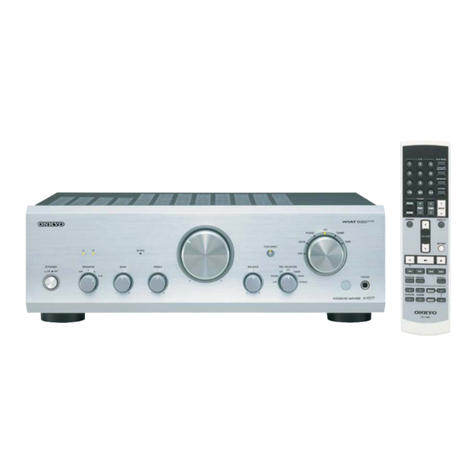
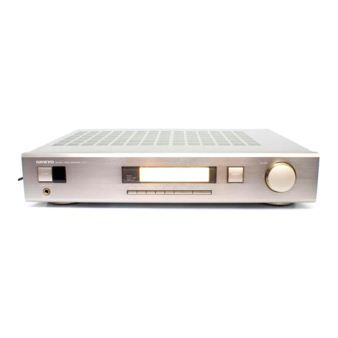
Onkyo TX-910 User manual

Ref.
No.
3443
ONXYO
SERVICE
MANUAL
QUARTZ SYNTHESIZED
TUNER AMPLIFIER
MODEL
TX-9
10
MODEL
TX-930
Black and Silver models
1
BHMD, BHMDN
1
120V AC, 60Hz
1
BHMP, BHMPF, MP, MPF
1
23OV
AC,
50Hz
1
l20V
or
220l ACiO/6OHz
1
SAFETY-RELATED COMPONENT WARNING!
!
COMPONENTS IDENTIFIED BY MARK
d
ON
THE SCHEMATIC DIAGRAM AND IN THE PARTS
LIST ARE CRITICAL FOR RISK OF FIRE AND
ELECTRIC SHOCK. REPLACE THESE COMPO-
NENTS WITH ONKYO PARTS WHOSE PART
NUMBERS APPEAR AS SHOWN IN THIS
MANUAL.
BHMQA
MAKE LEAKAGE-CURRENT OR RESISTANCE
MEASUREMENTS TO DETERMINE THAT EXPOSED
PARTS ARE ACCEPTABLY INSULATED FROM
THE SUPPLY CIRCUIT BEFORE RETURNING
THE APPLIANCE TO THE CUSTOMER.
240V AC, 50Hz
I
ONKYO
I
TABLE
OF
CONTENTS
Printed circuit board view from bottom side
...................
23
Schematic diagram
~~d~lTX-930
..........................................................
7-
,
D
Model TX.910
..........................................................
2
9
Printed circuit board-parts list
~~d~l~x.930
..........................................................
35
Model TX.910
..........................................................
38

SPECIFICATIONS
AMPLIFIER SECTION
Power Output:
Dynamic Power Output:
Continuous Power Output:
Total Harmonic Distortion:
IM Distortion:
Damping Factor:
Frequency Response:
RIAA Deviation:
Sensitivity and Impedance:
Phono Overload:
Signal-to-Noise Ratio:
Tone Controls:
Muting:
LOUDNESS (-30dB):
TUNER SECTION
FM:
Tuning Range:
Usabls Sensit~vity:
50dB Quieting Sens~tivity:
Caputure Ratlo:
lmage Rejection Ratio:
IF Rejection Ratio:
Signal-to-Now Ratio:
Atternate Channel
Attenuation:
Selectivity:
AM suppression Ratio:
Harmonic Distortion:
Frequency Response:
Stereo Separation:
Muting Level:
AM:
Tuning Range:
Usable Sensitivity:
lmage Rejection Ratio:
IF Rejection Ratio:
Signal-to-Noise Ratio:
Harmonic Distortion:
TX-930
60 watts per channel, min. RMS. at 8 ohms, both
channels driven, from 40Hz to 20kHz. with no more
than 0.2% THD.
2 X 100 watts at 4 ohms
2 X 75 watts at 8 ohms
2 X 80 watts at 4 ohms. lkHz (DIN)
2 X 65 watts at
8
ohms. lkHz (DIN)
0.2% at rated power
0.1% at 30 watt output
0.2% at rated power
0.1% at 30 watt output
50 at 8 ohms
20
-
30,000 Hz
f
1dB
20
-
20.000 Hz
f
0.8dB
Phono: 2.5mV/50 kohms
CD/Tape Play: 150mV/50 kohms
Tape Rec: 150mV/3.5 kohms
120mV RMS at IkHz, 0.2% TDH
Phono: 80dB (at 5mV input, IHF-A)
CD/Tape: lOOdB (IHF-A)
Bass:
f
lOdB at lOOHz
Treble:
f
10dB at lOkHz
-
03
f7dB at 70Hz. +5dB at lOkHz
-230V/Worldw1de models-
87.50-108.00M Hz (50kHz steps)
87.5-108.00MHz (50kHz steps) or
(200kHz steps) (Worldwide model)
Mono: 12.4dBf. 1.2pV. 75ohmd
1.2pV (S/N26dB, 40kHz Devi.)
75ohms DlN
Stereo: 19.2dBf. 2.5pV. 75ohms
25pV (S/N 46dB, Devi.)
75ohms DIN
Mono: 18.2dBf. 2.2pV. 75ohms
Stereo: 38.2dBf. 22
p
V, 75ohms
1.5dB
85dB
90dB
Mono: 70dB
Stereo: 65dB
50dB DIN (f300kHz. 40kHz dev.)
50dB
Mono: 0.15%
Stereo: 0.30%
30-15,000Hzf 1.5dB
40dB at 1kHz
30dB at 100-10,000Hz
17.2dBf. 4pV
522-1610kHz (9kHz steps)
522-1610kHz (9kHz steps) or
530-1710kHz (10kHz steps) (World wide model)
30 p V
40dB
40dB
40dB
0.8%
GENERAL TX-930
Dimensions (WXHXD)
:
455x120X316nm
17-15/16" X4-6/8" X12-7/16"
Weight: 8.0kg, 17.6Ibs.
TX-910
45 watts per channel, min. RMS, at 8 ohms, both
channels driven. from 40kHz to 20kHz. with no more
than 0.3% THD.
2
X 80 watts at 4 ohms
2 X 60 watts at 8 ohms
2 X 60 watts at 4 ohmsm, lkHz (DIN)
2 X 50 watts at 8 ohms. lkHz (DIN)
0.3% at rated power
0.1% at 30 watt output
0.3% at rated power
0.1% at 30 watt output
50 at 8 ohms
20
-
30,000 Hz
f
1dB
20
-
20,000 Hz
f
0.8dB
Phono: 2.5mV/50 kohms
CD/Tape Play: 150mV/50 kohms
Tape Rec: 150mV/3.5 kohms
120mV RMS at 1kHz. 0.3% THD
Phono: 80dB (at 5mV input. IHF-A)
CD/Tepe: lOOdB (IHF-A)
Bass:
f
lOdB at lOOHz
Treble:
f
lOdB at lOkHz
-
w
+7dB at 70Hz. +5dB at 10kHz
-1 20V model-
87.9-107.9MHz (200kHz steps)
Mono: 12.4dBf. 2.3pV
Stareo: 18.2dBf. 4.5
p
V
Mono: 18.2dBf.4.5
p
V
Stareo: 38.2dBf. 45
p
V
1.5dB
40dB
90dB
Mono: 70dB
Stereo: 65dB
50dB
Mono: 0.15%
Stereo: 0.30%
30-15,000Hzf l.5dB
40dB at lkHz
30dB at 100-10.000Hz
17.2dBf, 4pV
530-1 710kHz(lOkHz steps)

Remote control transmitter
RC-223s
Transmitter: Infrared
S~gnalrange: Approx.
5
meters (16ft.
X
4"
)
Power supply: Two
'AA'
batterles(l.5V
X
2)
Spec~f~cat~onsand features are subject to change without notice.
SERVICE PROCEDURES
1.Replacing the fuses
For
continuad protec~n
against
fire
hazard,rcplace
only
with
same
type
and
same
rating
fuse.
Ciuit
No. PanNo. Description
Model
Type
F901 252049 4A(STd)Srimary TX-910
MDMW
F901 252050 5A(ST-6)Snmary TX-930
MDMW
F902
252073 ~M-SE-EAK.R~IMIYTX-910
MP/MWMQ
F902 252075 25A-SE-EAKSnmary TX-930
MP/MWMQ
F951 252074 22-SE-EAKbC
outlet
TX-930
MP
2.Safety-check out
(Only U.S.A. model)
After correcting the original service problem.perform
the following safety check before releasing the set to
the customer.
Connect the insulating-resistance tester between the
plug of power suuply cord and nickel screw on the back
panel.
Specifications: 3.3Mohm
t
10% at 500V.
%Change of voltage
Worldwide models are equipped with a voltage selector to
conform with local power supplies. This switch is located
on the back panel. Be sure to set this switch to match
the voltage of the power supply in your area before
turning the power switch on.
This swith is set to 220V at the factory. Voltage is
changed by sliding the groove in the switch with the
screwdriver to the right or left. Confirm that the switch
has been moved all the way to the right or left before
turning the power switch on.
4.Step band selector switch
Worldwide models are equipped with a step band selector
switch. This switch is located on the back panel. This
switch is set to 50kHz (FM) and 9kHz (AM) at the factory,
but may have to be reset to lOOkHz and lOkHz depending on
the area where the unit is used.
De-emphasis FM step AM step
Europe: 50psec 50kHz 9kHz
U.S.A.: 75psec ZOOkHz lOkHz
5.Changing
the
band
step
With the exception of the models below, a
BAND
STEP
selector switch is not provided.
Shorted
Refer
to
thepage23.
c
MODEL
UD
UPAJQ
Q701
MICROPROCESSOR
l$l~lg
4
6.Memroy preservation
This unit does not require memory preservation batteries.
A built-in memory power back-up system preserves contents
of the memory during power failures and even when the
unit is unplugged. The unit must be plugged in and the
power switch turned on and off once
m
order to charge the
back-up system. Note that since this is not a permanent
memory,the power switch must be turned on and off a few
times each month to keep the back-up system operative.
The period of time during which memory contents are
preserved after power has last been turned off varies
depending on climate and placement of the unit.
On the average, memory contents are protected over a
period of
3
to
4
weeks (a minimum of
2
weeks) after
the last time power has been turned off. This period is
shorter when the unit is exposed to very high humidity or
used in an area with an extremely humid climate.
BAND
STEP
1OkHz-+9kHz
9&-lOkHz
R709(10kSZ)
Add
J732
Shorted
Cut
PARTS LIST
REF.
NO.
1
4
5
6
7
8
9
12
13
PART NO.
271
10749Y
27110750Y
281332541
27100228Y
271602931
27141441Y
27141442Y
27141443Y
27130643AY
27121686Y
27121687Y
27121689Y
DESCRIPTION
Front bracketass'y <B>
Front bracketass'y <S>
Back plate
Chassis
Radiator
Bracket
LH
Bracket
RH
Bracket
PC
Bracket,shield
Rear panel <D>
Rear panel
*
Rear panel <W>
KGLS-14RT,Holder
KGLS-12RT,Holder
3TTS+8B(BC),Self-lapping
screw
3TIW+8B,Self-tapping screw
4TTC+8C(BC),Self-tapping
screw
3lTP+8P(BC).Self-tapping
screw
3P+6FN(BC),Panhead screw
3SMS10W.SW+l4B(BC),Sems
Self-lappingscrew
Top cover
3TTS+8B(BC),Self-tapping
screw
Cushion
Spacer<P/W/Q>
Front panel ass'y <B>
Front panel ass'y <S>
End cap
L
End cap R
Clear plate
3TTP+8P(BC),Self-tapping
screw
Leg
3TTS+8B(BC),Self-tapping
screw
Knob,Loudness<B>
Knob,Loudness<S>
Knob,Level <B>
Knob,Level <S>
Knob.Volume <B>
Knob,Volume<S>
Knob.Power <B>
Knob,Power <S>
REF. NO. PART NO. DESCRIF'TION
86 28324170 Knob. SpeakerA <B>
28324172 Knob. Speaker A <S>
87 23824171 Knob. SpeakerB<B>
23824173 Knob. SpeakerB <S>
P902 25060054 TerminalGNU
W51
25050904
A
NSCT-2P697,AC
outlet
cQ>
2SA1265N-R,
2SA1265N-0,
2SA1491-0.
2SA1491-Yor
2SA1491-P,Power transistors
2SC3182N-R,
2SC3182N-0,
2SC3855-0,
2SC3855-Yor
U1 lA415525-3 NARF-4325-3,Tuner circuit
pc
board ass'y <D>
lA415525-3A
NARF-4325-3A,Tunercircu1t
pc
board ass'y <P/Q>
1A415525-3B NARF-4325-3B,Tunercircuit
pc
board ass'y <W>
U2 lA415526-3 NADIS-4326-3,Display circuit
pc
board ass'y <D>
lA415526-3A NADISd326-3A.Display circuit
pc
board ass'y <P/Q>
1A415526-38 NADIS-4326-3B,Displaycircuit
pc
board ass'y <W>
REF. NO. PART NO. DESCRIPTION
U3 lA415527-3 NAAF-4327-3,Power amplifiercircuit
pc
board ass'y <D>
1A415527-3A NAAF-4327-3A,Poweramplifiercircuit
pc
board ass'y <P/W/Q>
U4 lA415528-3 NASW-4328-3,Hcadphoneterminal
pc
board ass'y <D>
1A415528-3A NASW-4328-3A,Headphoneterminal
pc
board ass'y <P/W/Q>
U5 lA415529-3 NASW4329-3,Power switch
pc
board ass'y
U6 lA415530-3 NAETC-4330-3,Terminal
pc
board
U7 lA415531-3 NAPS4331-3,Power supply circuit
pc
board ass'y <D>
lA415531-3A NAPS-4331-3A,Power supply circuil
pc
board ass'y
<P>
lA415531-3B NAPS4331-3B.Powersupply circuit
pc
board ass'y <W>
1A415531-3C NAPS-4331-3C.Power supply circuil
pc
board ass'y <Q>
118 lA415532-3 NAETC-4332-3.Outlet terminal
pc
board ass'y <D>
U9 lA415533-3 NAETC-4333-3,Outletterminal
pc
board ass'y
<P>
lA415533-3A NAETC-4333-3A.Outlet terminal
pc
board ass'y <W>
U10 lA415534-3 NAAF-4334-3,Tonecontrolcircuit
pc board ass'y <D>
lA415534-3A NAAF-4334-3A,Tonecontrolcircuit
pc
board ass'y <P/W/Q>
U11 lA415535-3 NAETC-4335-3,Volumecontrol circuit
pc
board ass'y
U12 lA415537-3 NAETC-4337-3,Terminal
pc
board ass'y
U13 lA415538-3 NASW-4338-3,Voltageselector switch
pc
board ass'y <W>
NOTE: <B>:Blackmodel only
<S>:Silvermodel only
<D>:120V model only
<P>:230Vmodel only
<W>:Worldwide model only
<Q>:240V model only
ARE CRITICAL
FOR
RISK
OF FIRE
AND
ELECTRIC
SHOCK.
REPLACE
ONLY
WITH


PARTS LIST
REF. NO.
1
4
5
6
7
8
9
12
13
PART NO.
271
10763Y
27110764Y
281332541
27100228Y
27160272AY or
27160290Y
27141441Y
27141442Y
27141443Y
27130643AY
27121691Y
27121692Y
27121694Y
DESCRrnION
Front bracket ass'y <B>
Front bracket ass'y <S>
Back plate
Chassis
Radiator
Radiator
Bracket LH
Bracket
RH
Bracket
PC
Bracket, shield
Rear panel <D>
Rear panel <P>
Rear panel <W>
27121b95Y Rear panel
<Q>
14
27300750
&
Bushlng,conf
KGLS-14RT.Holder
KGLS-12RT,Holder
3nS+8B(BC),Self-lapping screw
37TW+8BVSelf-tappingscrew
4'TTC+8C(BC),Self-lapping
screw
31TP+8P(BC),Self-tapping
screw
3P+6FN(BC),Pan head screw
3SMSlOW.SW+I4B(BC),
Self-lapping screw
Top cover
3nS+8B(BC),Self-tapping screw
Cushion
Spacer <P/W/Q>
Front panel ass'y <B>
Front panel ass'y <S>
End capL
End cap R
Clear plate
3TTP+8P(BC),Self-tapping
screw
Leg
3TTS+8B(BC),Self-tapping
screw
Knob. Loudness <B>
Knob, Loudness <S>
Knob, Level <B>
Knob, Level <S>
REF.NO. PART NO
83 28324163
28324182
85 28324140
28324184
86 28324170
28324172
87 23824171
23824173
DESCRIPTION
Knob,Volume<B>
Knob.Volume
<S>
Knob,Power <B>
Knob,Power <S>
Knob, Speaker A <B>
Knob, Speaker A <S>
Knob, Speaker B <B>
Knob, Speaker
B
<S>
Terminal GND
..
2SA1264N-R,
2SA1264N-0,
2SA1694-0,
2SA1694-Y or
2SA1694-P,Power amplifier ~ransistor
2SC3812N-R,
2SC3812N-0,
2SC4467-0.
2SC4467-Y or
2202256 2SC4467-P.Power amolifier transistor
U1 lA419525-4 NARF-43254,Tunercircuit
pc
board ass'y <D>
lA419525-4A NARF-4325-4A.Tuner circuit pc
board ass'y <P/Q>
lA419525-4B NARF-43254B,Tunercircuit pc
board ass'y <W>
NOTE:
THE
COMPONENTSIDENTIFIED
BY
MARK
h
ARE
CRITICALFOR RISK OFFIRE
AND
ELECTRIC
SHOCK.
REPLACEONLY
WITH
PART
NUMBER SPECIFIED.
REF.NO. PART NO.
U2 lA419526-4
lA419526-4A
lA419526-48
lA419527-4
1A419527-4A
1A419528-4
1A419528-4A
lA419529-4
1A419531-4
lA419531-4A
lA419531-4B
1A419531-4C
lA419534-4
lA419534-4A
1A419535-4
lA419538-4
DESCRIPTION
NADIS-43264,Display circuit
pc
board ass'y <D>
NADIS43264A.Display circuit
pc
board ass'y
<PIC)>
NADIS43264B,Display circuit
pc
board ass'y cW>
NAAF-43274,Power amplifier circuit
pc
board ass'y
<D>
NAAF-43274A,Power amplifier circuit
pc
board ass'y <P/W/Q>
NASW-43284,Headplione terminal
pc
board ass'y <D>
NASW-4328-4A.Headphone terminal
pc
board ass'y <P/W/Q>
NASW-4329-4,Powerswitch
pc
board ass'y
NAPS43314,Power supply circuit
pc
board ass'y <D>
NAPS43314A.Power supply circuit
pc
board ass'y <b
NAPS43314B.Power supply circuit
pc board ass'y <W>
NAPS43314C,Power supply circuit
pc
board ass'y <Q>
NAAF-43344,Tone conuol circuit
pc
board ass'y <D>
NAAF-43344A,Tone conuol circuit
pc
board ass'y <P/W/Q>
NAETC-4335-4.Volume conuol
pc
board ass'y
NASW-4338-4,Voltage seleclor switch
pc
board ass'y
<W>
NOTE: <B>:Black model only
<S>:Silver model only
<D>:120 V model only
<b:230V model only
<W>:Wolrdwide model only
<Q>:240 V model only

'LET

OTHER
MODELS
SPEAKER
OUTLET

BLOCK
DIAGRAM
MODEL
TX-910
120V
MODEL

OTHER
MODELS

IC BLOCK DIAGRAM AND DESCRIPTION
LM7001(PLL synthesizer and controller)
Phase Detector
PD1
XIN
XOUT
I
d
Shift Register
.
Latch
1
h
I
I
L
AL
3x
4'6
511
CE
CL
DATA
Pin
No.
1
2
3
-.
.
4
.-
5
6
7
8
9
-
-
-.
.
-
10
11
12
13
14
I5
16
Terminal
XOUT
XIN
-
-.
CE
CL
DATA
-
SYN
-
,\LT(1/MOI\:O
--
Em
-~
-
B03
AMIN
FMIN
VDD1
VDD2
PDl
PD2
Vss
Description
Connect to the
7.2
MHz crystal oscillator.
Chip enable terminal. Connect to the
PLL
terminal of micro processor.
Serial clock input terminal. Connect to the CLOCK terminal of micro processor.
Serial data input terminal. Connect to the
DATA
terminal of micro processor.
Not used.
Auto/Mono control output terminal.
'H"
when Auto.
FM control signal output terminal. "L" when FM.
AM control signal output terminal. "L" when
AM.
AM local oscillator input terminal.
-
FM local oscillator terminal.
Power supply terminal for back-up.
Power supply terminal.
Charge pump output of the phase detector which constitutes the PLL. High level is output when the
divided local oscillator frequency is high than the reference frequency.
In the opposite case, low level is output. Floating occurs when the frequencies matched.
The output is applied to the variable capacitor diode in the local oscillator through the low pass
filters.
Ground terminal.

p
PD17103CX-528(Remote control decoder)
Bus
Q703
Transmitter Remote control
decoder
Infrared
RESET
REMIN
-
POW
a
PH SENS
-,
PODl
4
POWER
-
POD2
SYSIN
-*
POD3
9
GND
POB2
-
STAND-BY
POBO
-,
VOL
IND
p
POC3
-
VOL UP
POC2
-
VOL DOWN
POCl
-
PHONO
POCO
-,
SYSOUT
Pin
No.
1
2
3
4
5
6
7
8
9
10
11
12
13
14
15
16
Symbol
XIN
XOUT
RES
POW
PODl
POD2
POD3
VDD
POCO
POCl
POC2
POC3
POBO
POBl
POB2
V,
Terminal
OSC
SYS IN
+B
?xmsu'r
PHONO
VOL DOWN
VOL UP
STAND-BV
GND
Description
Connect to the 8.00MHz ceramic oscillator.
System reset terminal. Active low.
Signal input terminal from preamp. for remote control. Active low.
Phono detection input terminal. Active low.
Stand-by detection input terminal. During low input, only the POWER code is decoded.
System code input terminal.
Power supply terminal.
Output at this terminal are the custom code (16bits) remote control code input to REMOTE
IN, data code (Ibits), and the serial code (12bits) that has been converted corresponding to
the decoded data code (8bits)
When the player PLAYIREEJECT is input,
a
high pulse of 200ms is output.
When the volume DOWN code is input, a high pulse of 120ms is output.
When the volume UP code is input, a high pulse of 120111s is output.
During the output of VOLUME UPIDOWN, a pulse
(m
250ms) is output.
(Not used.)
This is the display output for remote control reception. Output is low when decoded code is
being recieved.
STAND-BY indication terminal.
Ground terminal.

FL TUBE
TO MUTING SW OF TU MUT D7
TO MUTING SW OF
D6
PREOUT
D5
DI
I
_RESET 0704
PRESET
RESET
I
I
K3
-
-
0133 PLL
PLL SYNTHESIZER CL
AND CONTROLLER
AM
band
setting
AM
1OK
0
0*
1
Fnquency Channel
IC
Region Range space
Ewpc
522-1611kHz 9kHz
Japan
SaudiArabia
53
1-
1602kHz
9kHz
Ww
U.S.A.
530-1710kHz lOkHz
e%d
!2ii

.aa!m uaqm
,,H,,
yeq.ua 1ndqm3s Aaa
.aywuaw
,,H,,
*spa1lndlnoue3s Aax pue luaus8g
7mpruals~sqns
JOJ
pa1uo~1muuo3Jo1ellpso
'wnlON
3yxela3
.pupalpunaro
.ro~el[!%o3!rwa3
~HJIV~I'P
av
01
1muuo3
'7ml3uralsk
~~EIII
JOJ
paluo!1suuo3 ~o~el[pso
~UI~J~C)
pal3auuo3pmaiq
uopdu3saa
'aa!~~uaqm
,,H,,
*spqxuallndlno ue3s
B?
pue ~uaux8ag
uoydysaa
WX
1.m
SSA
ZX
'
IX
31
uogsund
PE
fx
Z€
I£
OE
6Z
'ON
q~
"S
9s
3s
PS
10qu~As
v
c
Z
I
'ON
qd

LA1266(FM
IF
and AM radio system)
FI
IF IF
LIP
IF 10.7112
I
I
STOP
OUT
IN
vcc
11-1-1
1-2-
5-6-7
DETEClOl
AM
MIX
I
F
IS
AI
I
R
F
AMP
WT
METER DR
1
VER
OSC
OSC
CllD
IN
OUT
AN7470(Stereo decoder)
STEREO
16
knz
To
38
kHz
TO
MONO SW DIVIDER
VCO STOP
I
PREAMP
t
I
LB1630
(Motor driver)
TRUTH
TABLE
Wait
OFF
OFF
Wait
i
IN
1
H
I
N2
L
OUT
1
H
OUT
2
L
MOTOR
Normal


LC7823/LC7823N(Analog switch)
p
PC1225H(Power amplifier driver) NJM4558D-X (Operation amplifier)

PACKING
VIEW
REF. NO.
1 PART NO. Description
29052559Y Master carton
box
<B> (TX-930>
29052561Y Master carton
box
<S>4X-930>
29052563Y Master carton
box
<B>OX-910>
29052565Y Master carton
box
<S>4X-910>
29091440BY Pad
L
29091441BY Pad
R
29100034A 850X650,Styrenebag
282301 Staple
29110071 PP
tape
261504 Adhesive
tape
Accessary
bag ass'y
29341795Y Instruction manual
<D>
29341797Y Instruction manual
<P/W/Q/c>
292111 FM antenna
<D/W>
292112 FM antenna
<P&>
29065462 FM antenna adaptor <W/Q>
232140 NMA-3057,AM
loop
antenna
25055040 CV-K-2,Conversionplug
<W>
3010054 UM-3.Two batteries
24140223Y RC-223S.Remote control transmitter
2010200 Cord RI
29100097 350X250,Styrenebag
29365019A Warranty card <N>
283580MJ Servicestation list
<N>
29365024A Wmtycard
<F>
29100107 Styrene bag for warranty card
<F>
NOTE.
<B>Blackmodel
only
<S>:Siva
model
mly
<D>:
12OV
model
mly
*mv
model
only
<w>:waldwide
model
only
<Q>:240V
model
mly
&>:USA.
model
only
cF>-fimch
model
only
<O:CPudian
model
only

ADJUSTMENT PROCEDURES
Preparation
1
.Input
FM
mono:
lkHz.75kHz
devi.,60dB/
p
V
FM
stereo:
lkHz,75kHz
devi.,60dB/
p
V
Pilot signal
19kHz7.5kHz
devi.
AM:400Hz
30%
mod.
2.0utputs
Connect the non-inductive type resistors of
8
ohms
to the speakerterminals Aunless otherwise noted.
3.Standard Knob Position
VOLUME
...................................
Maximum
.........
BASS/TREBLE/BALANCE ..Center
..................
MUTING/LOUDNESS Off
.....................
INPUT SELECTOR
CD
SPEAKERS
................................
A
Confirming Operation
1
.Protectioncircuit
a.Speakerrelay
The speaker relay turns on after the power switch turned on for
5
minutes.
The speakerrelay turns off immediatelyafter the power switchturns off.
b.
Over-voltageconfiiation
The speaker relay is offirnmeditely after
DC
voltage
+
6V is applied to the terminal
CD.
Amplifier section
Idling Current Adjustment
Connect the DC voltmeter to the terminals
LID(RID)
and
CT
on the power amplifier
pc
board.
Adjust the semi-fixedresistor
R51l(R512)
so that the indication of voltmeter is
5
+0.5mV.
Note:( ):Right channel
=12
8
RID
e
=11
LID
vm
On
novcr
POWER
AMP-
PC
BOARD
SOLDERING SIDE
Other manuals for TX-910
2
This manual suits for next models
1
Other Onkyo Amplifier manuals

Onkyo
Onkyo A-8700 User manual

Onkyo
Onkyo TX-DS838 User manual

Onkyo
Onkyo M-5200 User manual

Onkyo
Onkyo A-8087 User manual

Onkyo
Onkyo TX-SV434 User manual

Onkyo
Onkyo A-9000R User manual

Onkyo
Onkyo TX-SV313PRO User manual

Onkyo
Onkyo Integra P-388F User manual

Onkyo
Onkyo R-100 User manual

Onkyo
Onkyo FR-N3X User manual

Onkyo
Onkyo A-8830 User manual

Onkyo
Onkyo A-8850 User manual

Onkyo
Onkyo TX-SV515PRO II User manual

Onkyo
Onkyo Integra P-388F User manual

Onkyo
Onkyo R-811RDS User manual

Onkyo
Onkyo M-282 - Amplifier User manual

Onkyo
Onkyo A-9070 User manual

Onkyo
Onkyo A-9110 User manual

Onkyo
Onkyo A-8037 User manual

Onkyo
Onkyo A-7 User manual