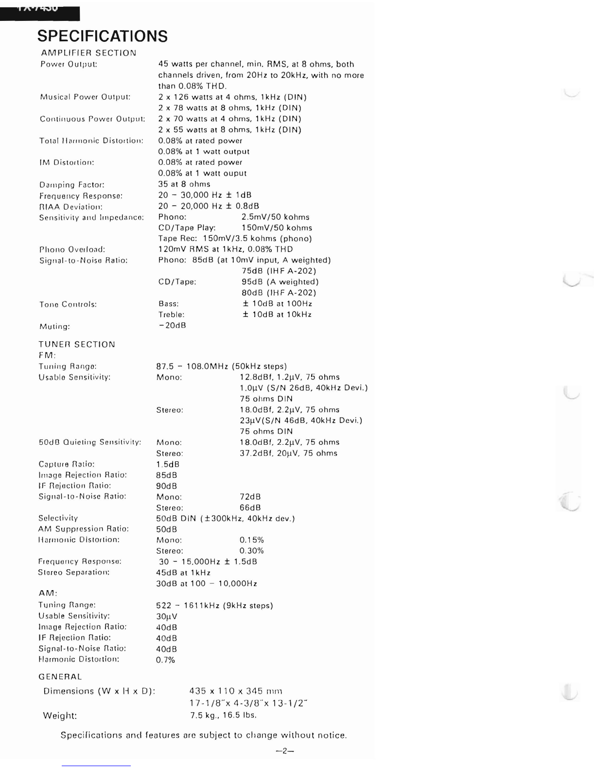
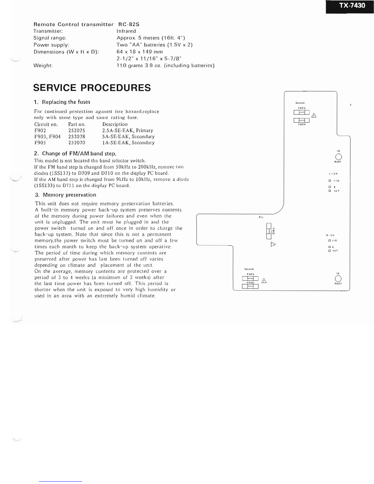
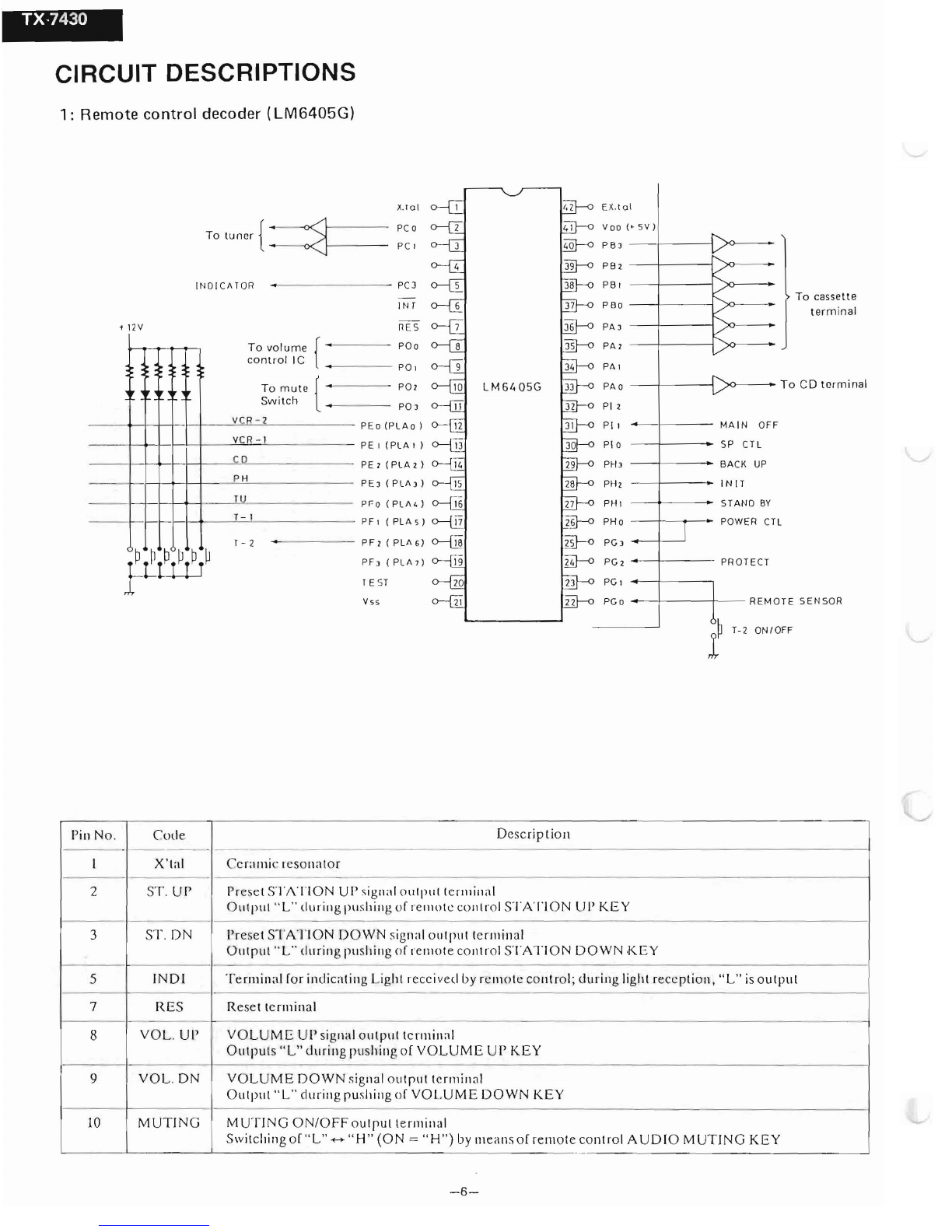
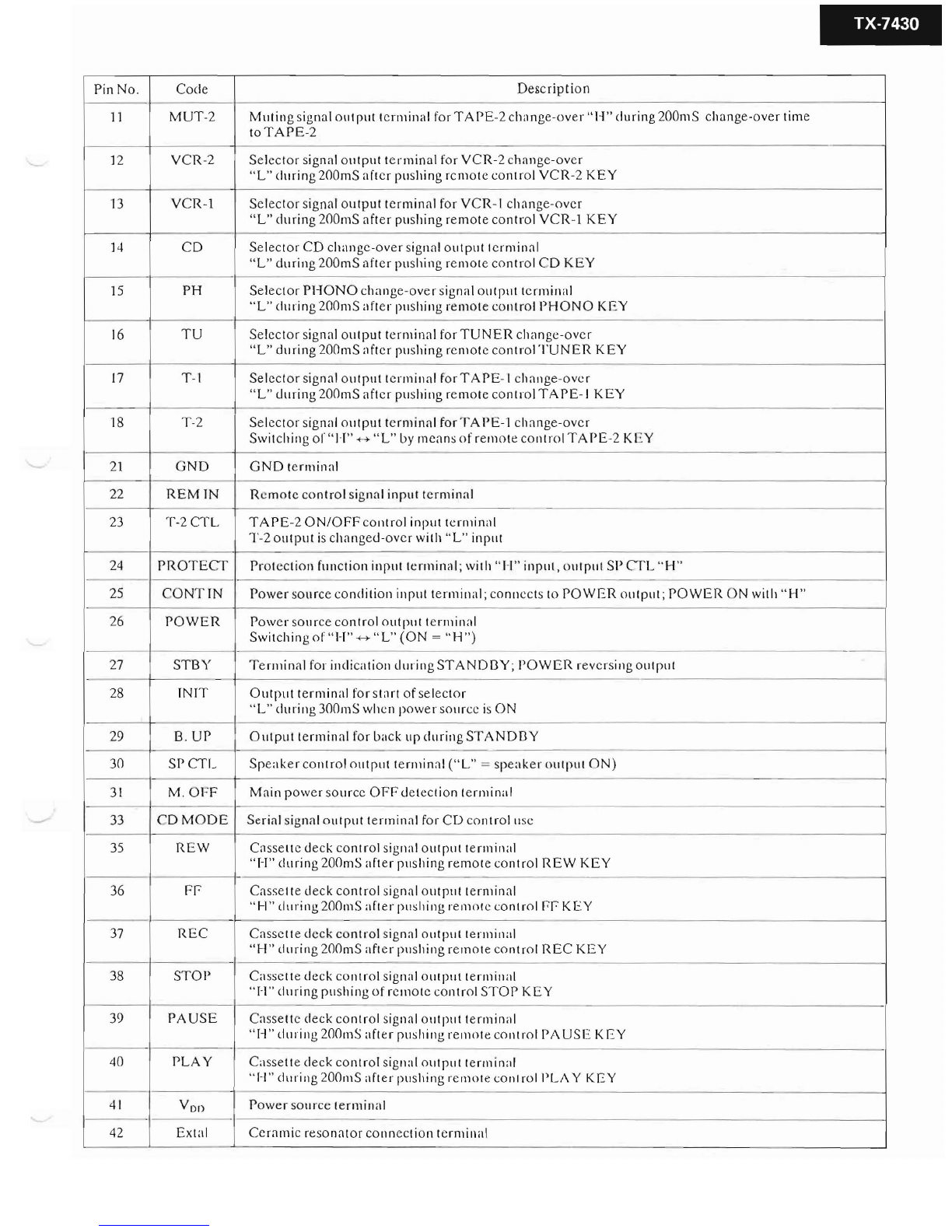
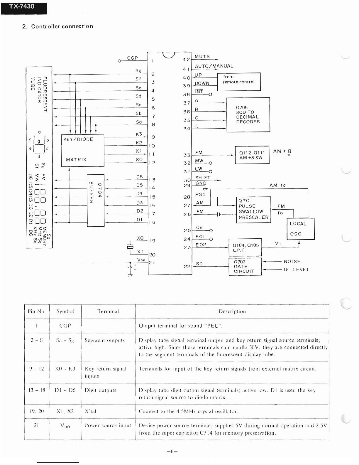
Onkyo TX-7430 User manual

TX·7430
SER
IAL
NO. 3258
ONKYO
,
~
,
SERVICE MANUAL
aUARTZ
SYNTHESIZED
TUNER AMPLIFIER
MODEL TX-7430
-
SAFETY-RELATED COMPONENT WARNING!!
COMPONENTS IDENTIFI ED BY MARK
L.
ON THE
SCHEMATIC DIAGR
AM
AND IN THE PARTS LIST ARE
CRITICAL FOR RISK OF FIRE AND ELECTRIC SHOCK.
REPLACE THESE COMPONENTS WITH ONKYO PARTS
WHOSE PARTS NUMBERS APPEAR AS SHOWN IN THIS
MANUAL.
MAKE LEAKAGE-CURR ENT OR RESISTANCE MEA-
SUREMENTS TO DETERMINE THAT EXPOSED PARTS
ARE ACCEPTABLY INSULATED FROM THE SUPPLY
CIRCUIT BEFORE RETURNING THE APPLIANCE TO
THE CUSTOMER.
TABLE OF CONTENTS
Specifications 2
Service procedures 3
Exploded view _. . . . . . . . . . . . . . 4
Parts list . . . . . . . . . . . . . . . . . . . . . . . . . . . . . . . . 5
Circuit description s 6
Block diagram - Amp. section - . . . . . . . . . . . . . . . 12
-Tuner section -
.,
. . . . . . . . . .
..
13
Block diagram
of
IC 14
Packing view
..
. . . . . . . . . . . . . . . . . . . . . . . .
..
17
Adjustment procedures __.
..
18
Pc bcard view/parts list
Power amp . . . . . . . . . . . . . . . . . . . . . . . . . .
..
21
FM
/AM tuner 25
Display . . . . . . . . . . . . . . . . . . . . . . . . . . . . . . 29
Preamp. . _. . . . . . . . . 30
Remot e cuntrol . . . . . . . . . . . . . . . . . . . . . . . . 31
Switch
31
Spea ke r 32
Volume 32
Schematic diagram
Amp. section " 23
Tuner section 27
Disassembling prccedu res 33
ON
KYO
®
AUDIO
COMPONfNTS
- 1-

SPECIFICATIONS
AMPLlr-IER
SECTION
Power
Output
:
Musi
c
~1
Power
Output
:
Continuous
Power
Outp
ut:
Total
l larmo nic Dis tor tio n:
IM
Distort
ioll
:
D~rllping
Factor:
FroClu8
11
CY
Responso:
RIAA
Ouvia tio n:
Se
ns iti vit v
aud
lmp
cda nco :
Pho
no
Ovet lo ad:
Signal-lo-Noisu
Ratio:
Tone
COIlIIOls:
MUl
ing:
TUNER
SECTION
FM
:
Tuning
Rango :
Usabio
Sunsiti
vitv:
50cJO
Ouio rinp
Snnsitivitv
:
Captute Ralio:
Imago Hei
ectiou
Ratio:
Ir: Rojocli
oll
R~lio:
Signal
-lo
-Noiso Ratio:
Selecti vity
AM
Suppression
Ratio:
ll arruo
nic
DIslortion
:
Fro
quuncv
Rosp
onso
:
Storeo Separ ari on:
AM:
Tuning
Rango:
Usable
Sensitivitv:
Image Rejo
clion
Hario:
IF Rejeclion
Ralio
:
Signal
-Io-Noise
Ratio :
Harmonie
Otstoulou:
GENERAL
Dimensions
(W
x H x
D):
Weight:
45
watts
per
channel,
min.
RMS.
at 8 ohrns,
both
channels
driven
. from
20Hz
to
20kHz.
w ith no
more
than
0.08% TH D.
2 x
126
watts
at 4
ohrns.
1kHz
(DIN)
2 x 78
watts
at 8 ohms,
1kHz
(DIN)
2 x 70
watts
at 4
ohms,
1kHz
(DIN)
2 x 55
watts
at 8
ohrns,
1kHz
(DIN)
0.08% at rated
power
0.08% at 1
watt
outpur
0
.08
% at
rate
d
power
0.08% at 1
watt
ouput
35 at 8
ohms
20 - 30
.000
Hz ± 1
dB
20 -
20.000
Hz ± 0
.8dB
Phono
:
2.5mV/50
kohms
CD/Tape
Play:
150mV/50
kohms
Tape Rec:
150mV/3
.5
kohms
(phono)
120mV
RMS
at 'lkHz,
0.08%
THD
Phono
:
85dB
(at
10rnV
input
, A
weighted)
75dB
(IHF
A-202)
CD/Tape:
95dB
(A
weighted)
80dB
(IHF
A-202)
Bass: ±
10dB
at
100Hz
Treble:
±10dBatl0kHz
-20dB
87.5 - 108
.0MHz
(50kHz
steps)
Mono
:
12.8dBf.
1.2~V.
75
ohms
1
.0\lV
(S/N
26d
B.
40kH
z
Devi
.)
75
ohms
DIN
Stereo: 18
.0dBf.
2
.2~V.
75
ohms
23~V(S/N
46dB.
40kHz
Devi.)
75
ohms
DIN
Mono:
18
.0dBt.
2.2~V.
75
ohms
Stereo:
37.2dBf
.
20~V.
75
ohms
1
.5dB
85dB
90dB
Mono
:
72dB
Stereo:
66dB
50dB
DIN
(±300kHz
.
40kHz
dev.)
50dB
Mono
:
0.15
%
Stereo: 0.30%
30 -
15.000Hz
±
1.5dB
45dB
at 1kHz
30dB
at
100
- 10
.000Hz
522
- 1611 kHz
(9kHz
steps)
30~V
<lOdB
40dB
40dB
0.7%
435
x 110 x
3<15
m[n
17
-1/S"
x
<1
-3/S
"x
13-1/r
7.5 kg.. 16.5 Ibs.
Spec
llicatiorts arid Ieatures are
subject
to
chanqe
without
notice.
-2-

TX·7430
Remote
Control
transmitter
RC
-82S
Tr
ansmiu
er:
Inlrar
ed
S
ign
nl range:
Appr
ox. 5
meters
(1
6ft.
4")
Power
supply:
Two
"AA"
baueries
(l
.5V x 2 )
Dim ensrions (W x H x
0)
: 64 x 18 x
149
mm
2-1/2"
x
11/16"
x
5-7/8
"
Weight
:
110
grams 3.9 oz.
(in
clutl
ing
uaueri
es)
SERVICE PROCEDURES
1. R
eplacing
the
fuses
f or co nt
inucd
prrn
cc tion ;);:;Ullst lir c ha za rd.replnc e
0111\' w ith saure tvpe
and
s.uuc
rat
ing (use.
Circu it no.
Part
no. Des
cripti
on
f9
02
25207
5
2.5A-SE
-EAK, Pri
mary
f903
, P9 04
252078
5A-SE-EAK,
Sec
ondary
P905
252070
lA-SE-EAK
, Scc
ondary
2.
Change
of
FM/AM
band
step.
This mo de l is not loca red Ihe band sclcc to r swilch.
If th e PM b
and
step is eha nged from
50k
Hz 10 200k Hz , rcm ovc rwo
died es
(lSS133)
to
07
09 and
0710
on th e display PC boar d.
If th e AM
band
stcp is chungcd from
9kH
z to 1
0kHz,
rernov
e
01
diodc
(lS
S133)
10
0711
on
the displuy PC board.
3.
Memory
preservati
on
Th
is un it
does
1I
0t req uire m
emor
y pr
eserva
tion b
au
cries .
A hu il
t-
in me
mory
p
ower
bac
k - up sy stem prese
rves
co nten ts
01 th e m
emory
durin
g p
owe
r
lailur
es
and
eve
n when t he
Pli
.
unit
is unplugged .
Th
e unit
rnust
he pl
ugge
d in
and
the
power sw itch t
urn
ed Oll and
oll
on ce in order to
char
ge the
ba ck
-up
system. No te rhnt since this is not a
perma
nent
mem ory ,the pow
er
switch rnust be
turn
ed
00
and off a few
times
eac
h
mont
h 10
keep
the back
-u
p sy stern ope ra
tive
.
Th
e
per
iod of time
dur
ing
whic
h mem ory co
nte
nts ar e
preserved
after
pow
er
has
last
been
turned off va ries
d
cpen
din g on
climat
e
and
placement
of th e
unit.
On the
ave
r
age,
mem ory contents
ar
e pro tec ted
over
a
peri od of 3 10 4
wee
ks (a mi
nimu
m of 2
wee
ks) af ter
the last time pow
er
has been
turncd
off. T his pe
riod
is
shor l
er
when
the
un it is ex
pos
cd to very high
hum
idit y or
used
in an arc a
with
an ex tremel y
humid
clima te.
o I I 0
o ,
o
0 110
0'
o vc r

TX·1430
o
0 '
Q
-
>
C
;:
W
W
C
o
--I
a.
><
w
-4-

PARTS LIST
REF.NO
. PART NO.
DESCRIPTION
Al
27100
121 A Chassis
A2 27
1209
43 A Back panel
A3 27 13 0470 Bracket , shie lded
A4 27 130 46 8A Bracket, rad iat or
A5 27
16020
1
A6
27130
469
A
A8 27
190
359
A
A9
272
73
030C
A
I0
28 133
176A
A l l 2
8130242A
A12 27
300750
A13
27141122
AI4 27 14 1123 A
A15
272702
16
A2 1 27
110338
8
27110339
8
A22 27
190525
27
190526
A23 27
190
105
A3 1 28 18
4356A
28
184357A
A51 l AOO1121
lA
OI0 12 1
A52
28140
220
A61 27 175 13 0
A71 2832
2796
283 22795A
A72 28
322469
28322304 -1
A73
28322
470
2832230
5-1
A74 28
322
92 2B
283
22923B
A75
28322928
28322929
A76
2832292
4
28322925
A77
28322926A
28322927
A
BI 834
430068
B2 83 1
1300
88
B3 838 4
4008
9
B4 834
4301
08
B5 82 1
4300
6
B6 8304
40089
B7 82 1
4200
4
833430080
B9
8800
11
BIO
830
440109
Radiator
Bracke
t, po wer transforrner
Holder, dial plat e
Join t L
Back
platc
Dial plate
~
Strainrclicf
Bracket
F
Brack et R
Spacer
Fro nt bracket ass 'y < S>
Front br acket ass'y < B>
H
older,
slide r < S>
Hold er, slider < B>
H
old
er, ante nna
Top cover <
S>
Top cove r < B>
Fr
ont
pane
l ass'y <
S>
Fro nt pa nel ass'y < B>
Cushion
Leg
Knob,
Power < S>
Kno b, Power < B>
Knob,
Speak er A <
5>
Knob
, Speakcr A
<8
'>
Kriob , Spcaker B
<5
>
Knoh, Speaker II
<B>
Knob, Volun••
$'
Kno b. Volume < B>
Kn ob, Ton e < S>
Kno b, T on e < B>
Knob, Slide <5>
Knob, Slide < B>
Knob , Push <S>
Knob , Push < B>
3T r S+6B(BC),
Tappi
ng scrcw
3Tn \'+8f\, Tapping scrcw
4TTB"'SC( BC), Tap ping screw
31TS+I0B
(B(' ), Tapplug screw
3P+6 FN(BC), Pan hcad screw
4TTC+8C(BC),
Tapp
ing screw
2P+4F(BC), Pan
hcad
screw
3TTP+
8P(BC),
Tapping
screw
Rivet
4TT
C+I 0C(BC),
Tapping
s
crew
REF .NO.
Bll
F902
F90 3,
1"
904
1"
905,
F906
P304
P901
Q508
, Q608
Q509,
Q609
Q902
,
Q905
T901
UI
PART
NO.
870060
252074
252078
252070
250600
44
253 128B or
2531
30A
220 178 3,
2201 784 or
2
201786
220
1773,
220
1774 or
220
1776
2201 754 ,
220
1755
,
22014040
r
220
1405
2300
199
I A008569 ·2A
U2 I A008570·2A
U3
IA
0085
71·
2A
U4 I AO
I3572
·1
U5 1A01 3573-1
U6 l
A013574
·1
U7
lA0
08575-2A
UR I A01 3576·1A
U9 I AO
I3577
·1 A
UI0
I A008578·2
Ull
1A008579-2
DESCRIPTION
Flat washer
~
2A-SE-EAK, Fuse, prirna ry
~
5A-SE-EAK , Fuse, secondary
~
1A-SE-EAK, Fuse, secon
dary
Termin
al GND
~
AS-CEE, Power
supply
cor d
2SC3854(0),
2SC3854(Y)
or
2SC3854(P)
2SAI490(0),
2SA
I490(Y
) or
2S AI4
90(
P)
2SDI9 13( R) ,
2SDI9
13(S),
2SDI
406(Y)
or
2S DI
406(G
R)
.6.
NPT-955G, Power transformer
NAAR-2869-2 A, FM/ AM
tune
r
pc b
oard
ass'y
NADlS-2870-2A
, Display pc
b
oard
ass'y
NAAF-2871-2A,
Prearnpli f'ier pc
board
ass'y
NAAF-2872-1,
V
olum
e pc boa rd
ass'y
NAETC-28 73-1 , V
olum
e rnotor
pc board ass'y
NAD IS-287 4-1, Vo l
ume
in
dicato
r
pc
boa
rd ass'y
NAPS-2
875
-2A, Power
amplifi
er
and
powe
r
supp
ly pc
boar
d ass'y
NASW-2876-1A,
Speake
r switch
pc
boar
d ass'y
NAETC-2877 -1A,
Speaker
termina l
pc bo ard ass' y
NA
ETC-2878-2,
Rem
ot
e contro l
terminal pc
board
ass' y
NAAF-2879-2,
Switch
pc
boa
rd
ass'y
NOTE:
<B>:
Only Black mo del
<
S>:
On ly Silver mo de l NO TE:
TH
E
CO
M
PON
ENTS
IDE
N
TIF
IE D BY
MARK~
AR
E
CR IT ICA L F
OR
RISK O F FIRE AN D
ELE
CTI C
S
HOCK
.
REPL
A
CE
ON LY WIT H P
ART
NU MBE RS
SP
EC
IFIE D .
88

---
-- - - - --
--
----
---
CIRCUIT DESCRIPTIONS
1:
Remote
control
decoder
(LM6405G)
x.i o t
o---E
Ta
tun nr {
- -
INDIC fl TOR
-
-t-
- - - ..
-
-t-
-
-r-
-PHo
PE, ( PLfI , )
-~
---
..
PEo
(PLA
O)
f---
---
PE I (P
LA'
)
-
~---
..
T -2 PG ,
Ph
(P
Lfl7)
PG2
..
-
+-
---
P
G,
PHI
TEST
PH,
PGo
-
~---
-+-
-
-
t
PA '
PA>
POo
po,
PAO
-
~---
-j
P
I2
PB
2 -
-I
,----- -
-j
)
0--
PB I
PC]
po ,
Pl
I
PI O
PH,
P
A'
IN T P Oo
--I
'---
-
--j
V
oo(
'5V)
PCo
PB'
- - f-- -
-I
;>0
EX
.la
l
PF> ( PL fI
.)
pc
,
~ES
po>
PE > (P LA 2 )
~
f----
Vss
Ta v
alu
me [
can
tra
l lC
Ta
mut
e [
r Sw
itc
h
..
VCR - 2
VCR - ,
c.p
PH
---.-L!J
T- I
Ta casset te
t
erminal
• 12V
;,.0---
-Ta CD term inal
LM 64
05G
M
AIN
OFF
SP CTL
BACK UP
I N I T
STAND BV
POWER CTL
PROTEC
T
REMOTE S
ENSOR
T- 2 ON IOFF
Descrlpti on
!'ill No . Code
X't al Ccr.unic rcso ua tor
I
Pr
oset
STATION
U!'
sigIlai o utput
ter
min
al
O utput
"L
"
durin
g pu
shin
g o f rc mo tc co n tro l ST AT
IO
N LiI'
KEY
2
ST.
ur
l'r
esct S
TATION
D
OWN
sig nal
outpur
te
rmin
al
Output
"
L"
durin
g pu
shillg
o f rc
mote
co utro l ST
AT
IO
N D O W N K
EY
3 5
1'.
D N
(NDI
T
erminal
Ior
indic ntiug Light re cci v
ed
by r
cm
otc
c
out
rol ;
during
liglu
rec
cpti
on
,
"L
" is
output
5
7 Re
set
termin
al
RE
S
VO L.
U!'
V
OLUME
U!'
signa l o utpur tc
rmiu
al
Outputs
"L"
during
push
ing of
VOLLiME
ur
KEY
8
VOL.
DN
V
OLUM
E D
OW
N signa l outpur t
erm
inal
OUlpUI " LU
durin
g pu
shing
o f
VOI.UM
E
DOWN
KE Y
9
10
MUTIN
G
MUTI
NG
O
N/OFF
oUl
pull
erlllinal
Switchin
g
of
" L"
++"
H"
(ON
= "
H")
by nieans of
renr
ote
co ntro l A
UDI
O M
UTIN
G K
EY
-6-

TX-7430
Pin
No .
Code
Descrlprion
11
MUT-2
Muting
signal
out
put
terminal
for T A
PE-2
cha nge-ove r ''\-'1''
during
200mS
chang
e-over
tim e
loTAPE-2
Sele
ct
or
signal o utput te
rminul
f
or
VCR-
2 cha nge-ove r
"L"
during
200mS
aftcr
pu
shing
rcmote
contr
ol
VCR-2
KEY
12
VCR-2
13 V
CR
-1
Select
or
signal ou tp ut
terminal
for
VCR
-I change- ov c r
" L"
during
200mS
afr
er
pu
shing
r
emote
control
VCR
-1
KEY
14 C D
Select
or
CD
changc-over
signal
outpur
terminal
"
L"
during
200 mS aft
cr
pu
shing
r
emot
e
control
C D
KEY
Select
or
PHONO
chang
e-
over
signal
out
put
terminal
"L"
during
200mS
after
pu
shing
remote
co utrol
PHONO
KEY
Sele
ct
or
signal output t
erminal
for
TUNER
cha nge-o vc r
"L"
during
200mS
aftcr
pu
shing
renr
ote
control
TUN
ER
KEY
Selc
ct
or
signal o utput t
erminal
forT
A
PE
-I change- o vcr
" L"
during
200mS
after
pu
shing
r
emote
cont
rol
TAPE-I
KEY
Select
or
signal o utpul
terminal
for
TA
I'E-1 change-ovcr
Swit
chin
g
of
" J-I"+->" L" by
mcans
of rem o te co ntro!
TA
PE
-2 KEY
GND
terminal
R
cmote
control
signal
input
terminal
TAPE-
20N/OFF
control
input
terminal
1'-2
outpur
is
chang
ed-ov
cr
wiih
"L
"
input
Pror
eeti on
function
input
terminal;
with
"
J-I
"
input
,
out
put
SI'
CTL
" H"
Power
so urce
condiiion
input
terminal
;
conn
ccts to
POWER
output
;
POWER
ON
with
"
H"
15
PH
16 T U
17
1'
-1
18
1'-2
21 G ND
22
REMIN
23 T -
2CTL
24
PRO
TECr
25 CO
NT
IN
26
POWER
Power
so urce
control
outpur
terminal
Switching
of
"H"
+->
"L"
(ON
=
"H
")
27
STBY
--
T
erminal
f
or
incli
cati
on
during
STANDI3Y
;
POWER
rever
sing
outpur
Output
t
erminal
for
stnrt
of
s
elector
" L" c1ur
ing
300mS
wh cn pow
er
so urcc is
ON
O utput
terminal
f
or
back
up
during
S
TANDI3Y
Speaker
c
ontrol
outpur
terminal
(
"L
" =speake r o utput O N)
28
INIT
29 B .
UP
30 SP
CTL
31 M .
OFF
Main pow
er
sour
cc
OFF
det
cction
t
ermina
I
S
erial
signal
outpur
t
ermin
al f
or
CD
co ntrol usc
Cassett
e
deck
controi
signal
outpur t
erminal
"H"
during
200m
S aft
er
pu
shing
rernore
conrr
ol
REW
KEY
33 CD
MO
D E
35
REW
36 Fr -C
asse
ue
d
eck
control
signal o utpul te rminal
" H"
tluring
200mS
after
pu
shing
rern orc
cont
rol
rr
K
EY
C asse tte deck c
ontrol
signnl outpur
terminal
" H"
durin
g 200mS a fte r pu
shing
r
em
ore
cont
rol
REC
KEY
C assc tte
deck
c
ontr
ol
signal
o utput
terrninnl
"H"
ehrring pu
shing
of
rcin
orc co ntro l ST O P K
EY
Ca
ssett
e d
eck
control
signal o utpur t
erminal
"/-I"
timin
g
200mS
after
pu
shing
rem
ote
cout
rol
PAUS
E K
EY
Cass
ette c1eck
contr
ol signal o utp ur t
ermin
al
"
1-1
"
durin
g
200m
S a fte r pu sh ing renr ot e
cont
r
oll'LA
Y
KEY
37
REC
38
STOI'
39
PAUSE
40
PLAY
41 Von P
ower
so
urce
terminal
Ccr
ami
c re
sonator
c
onnccti
on
terminal
42 Extal

TX-7430
2.
Controller
co nnectio n
\..T CGP
Sg
-;
--"
c z r
rn
~c
rn
()O
!>JJ
-:i m
O (J)
JJ()
rn
z
-;
SI
Se
Sd
Se
Sb
f
0
Ig ib
-. l
KE
Y/O
/OOE
So
K3
K2
el
--
le KI
d MATRIX
KO
(J)
_ (J)
<0
0 ;:: -"
(J)
::E3:
0
__
(Jl
~
C
D
GlI-I-1
o
~
-
(J)
0 1- 1- 1
N - -
~
C
D
;>;
;:: ;::
OII
m
O)N
N
~(f)
(J) (J) o c>-
0<0
JJ
-<
--
rn 0
C --J
-q
0
-" .l> -
m
.o -
L......-
5
T
06
05
04
03
02
0 1
XO
XI
Voo
!
~
\J
4 2
I
4 1
2 4 0
3 3 9
4
38
5
37
6
36
7
35
8
34
9
10
I I 3 3
12
32
3 1
13
30
29
14
/5
28
/6
27
17 2 6
18
25
24
19 2 3
20
2 1 22
MUT E
AUTO/MA NUAL
UP Irorn
DO
WN re
mot
e con trol
INT
A
B
070
5
BCD TO
C DECIMAL
D
ECODE
R
0
FM 0 1
12
, 0 111 AM + B
AM+BSW
MW
~
LW
SHIFT
~
AM 10
PSC I
AM I Q701
PULSE FM
FM 1
1--
SWALLOW 10 I
. PRESCALER LOCAL
CE
~
OSC
EOI
~
I
I
01
04,
0105
VT t
E
02
L.P.F.
I
07
03 . NOISE
SO GATE
I IF LEVEL
CIRCUIT
I'in No .
I
Symbo l
(
'(J
P
Te
rmi
nal
- - -
..
O utp ut t
erm
inal
Ior sound
- - - -
Dcscri
ption
'
'I'E
E'' .
2 - 8 S;l - SI' Segment
Oll
Iput s
Displ
ay tube
s
i
g
n
~
1
te
rmina
l ou tp ur an d kc y rc
ruru
signa l source te
rmi
nals:
activc high. Sincc Ihesc t
ermi
nal-, can h,lIl dle JO
V,
they are co nncc rcd d
irec
tly
to the seg
meut
terminuls
of
ih e tl u
or
escen t displa y
tub
e.
lJ - 12
-
KO - KJ Key return sigll<!l
inpui s Te
rmiuat
s ror in put o f thc key ret urn sigllals
lr
om extcrual
maui
x circuit.
D-
IS
IJI
-
1)6
D igit
ou
tpu
ls D isplay tubc digil out pul signal te n u iua is:
rc tur n signal sourcc to diodc
matri
x. nctive low. 0 1 is uscd the key
IlJ, 20 X I . X 2 X 'l al
Conu
ect 10 the 4
.5M
Hz
cry
sral oscil
lutor.
21 V DO Pow
er
sot I rce
inpu
t
Dev
ice powcr so1Irce tcrmi nal; slipplie5
5V
dnr
illg no rma l operanon and
[roru the super capaci tor C7 14 Ior memo ry preservat ion. 2.5 V
- 8-

TX-7430
Pin No .
Symb
ol Te rminal Dcscripiion
22 SO Sta tion det e
etor
signal input Input terminal for deteeting
whethcr
or not a brondcast signal is bcing
reeeived during uu
io-
tuning.
Stopped
by the high level.
2:\, 24 EOI, E02
Err
or ourpurs
Char
ge pum p ou tpur of thc phas e detecror with
cons
iirures the PLL. High
level is outpu t whcn t he dividcd oscillation frcqucucy is highcr rhan
ih
c
refcrencc frcqu cncy. In the op posiie case , low level is output. Floating
occ urcs whcn thc frcq ucucies match . T he o
utp
ur is npp licd 10 the varia ble
capaci
tor
diode in rhe fro nt
end
thr
ough rhc low pass filler Q
I04
and Q
I05
.
T he
ou
lp
ut from bot h tcrm iuals is same, but only E02 is usctl.
25 CE Chip
enab
le Deviee selcction signal input t
ermin
al. High lcvcl
l.ow level ... Memory presc rv.uion ... No rma l op era no n
26 FM FM local ose illator
slgnal
input
Input terminal [or FM loeal oscill.uor is divided by I/l o or 1/17 by prcscalcr
Q7()1.
--- ---
27 AM AM loeal oscillaror
signa l
inp
ut
Termin
al for input of ihe A M local oscill.uor signal.
2R PSC Pulse swallow
com rol ou tpu t Thi s t
ermin
al
outpu
ts a signal tluu swirchcs the presc.iler division r.uio of
Q70 1 to 1/10 or 1/17 when rhc pu lse swallow meihod is used [or division.
(FM only)
29 GNO
Grou
nd
---
-
30 S
HIFT
Preset rcve rsc
indieation ou tpur Te rminal for ind iennon ou tp ul whei her
MI - M8: Low lcvcl M9 - M 10: High MI - MS or M9 - MI Il the prese t key.
level
31
32
LW
MW
Band switching
signal ourputs
Terminal
s for signal outpul switehing of cach band. High level is outpul frorn
terminal of FM (pi n 11
0.
33) .md low lcve l is out put lro rn orher t erminals
(pin no. 31 & 32) duriug r M rece prion
33
34
35
30
37
r-M
A
B
C
0
Preset srarion
indica rion OUlpU
IS
Te
rmi nals for
MI M2
A I ()
n () I
C () ()
0 () ()
..
--
ßCO
code outpur of pre sct stutio n indic.
uor.
M3 M4 M5 MIl M7 MS
I () I 0 I ()
I () 0 I I 0
() I I I I ()
() () () () () I
3R INT Not
uscd.
39
MEMO
RY Mernory down
inpu t
Terminal
for down signal input of preset
Acrive low. mc m
ory.
-
,.j()
4 \
42
ME M
OR
Y
UP
AUTO
I
MANUAL
MUTE
Memory up
inpu
t
Au
to/Ma
nual
indi
cation
outp
ur
Muring outpu l
-
T
ermin
al for up signa l inpu t of pre sct memory.
Aciive low.
Te
rminal Ior irulication
output
whether or auto i he tuni ng mod e.
This t
erm
inal becom es high dm ing ,1
11
10 morle and low (hlring mununl mode,
Output t
ermin
al which
mute
s rhe shock noisc oeeurring whcn rhe PLL is
released; nctivc high. T in: muti ug signal is outpur as shown below.
UP/OOWN
of manu ul/auto moc le , presel Illelllory is reealled , b.uid swirching
ancl
preset
scan.

TX·7
430
Control key and diode matrix connections
K3('1) K2(
111)
KI
(II)
KII( 12)
' -
--
Sg(2)
M4 /M 14 M3 /
MIJ
M2/M 12 MI
/MII
Sr(3) MH
/MI
H M
7/M17
MU
M I(, M
5/M1
5
-
--
----
S
e(4)
I'IU
,SET
MIIJIM20
M3/M
IY
SC
A N
_ .
---
..
_-
-.
--
S
d(5)
S I-
f1n
LW M W " M
Sc(6)
A U
TO
M
EM
OI
~
Y
I)
OWN
UI'
MAN
UAL
Sb(
7) HI -l l L
l'NIJ
I) IS I'
I.A
Y
I'R
O
GI
~
A
M
W I
DEI
NA R
IW
W
--
---
---
-
Sa( H)
'l0/'ik
Hz '
LW
2 ' LW I
'A
M
- -
-----
[) I(I H) ' I3A N I) 0 ' IJA N D I ' I
11tH
ST
AT
IC/
DY
N A
•
Dio
de
111"1
rix rnblc I
llA
N DIl BA N D I
I
~E GI
O
N
FI~E
QUEN
C
Y
C I IA NN E L
H
AN
G E S
I'A
CE
-- - _ . -
D7 J0 1)70 '1
0 0 U S .A . R7.'1- 107.'1M Hz 200k H ,.
1 I Europe 87 .50-
I08
.00 M H z
50k
Hz.
A M IOkH ,J9
kH
z
FI~
E
Q
UE
N
C
Y
I
~A
N
GE
CII ANN EL SI'AC E
D711
lJ 0 530- 1620 kH z 10kH z
0
--
I
1
522
- 161l k
Hz
9k
Hz
11
53 1- I
W2k
Hz
'1k Hz
.-
0:
Op
en I:
Co
nue ct
the
diocle (I S
SI3
3) . tnhle 2
11
: Open I: Councct the diode ( 1
.'1.'1
133). iable 3
n A N DII,
DANDI
.. ..
"M
I" I/\(I oc llillgs . See tnble 2.
lO
/lIkH
z .
....
AM
I
,,"
\(I oe ll illgs . See tub le 3.
3. Muting circuit
lro m
mUl
in9 Ou
IPU!
0 ' c o o
trou
er rc
070
2 ri1\ '12
Lch
from
TKC
020
4
8
,-
- -
-,
0 106
011 2
0 7 15
R7 5 3 M
ONO
Reh
01 03
FM IF &
AM rad io
svstam
16
0 20 1
S
tereo
dec
oder
The
rn
uting
cir
cuit
operat es in the follo
wing
cases ,
1.Wb ile pi1l 4 2 of co ut roller IC ou t pu ls thc high lcvc l.
Q207
and
Q208 are
tumed
on and
muting
is
clo
sed in
the foll ow ing "cascs
.f
Ü
While
the manu al
UP
/DOWN
swi tch
is
being
held
down.
(2)When
a stat ion in th e m
emory
is
recalled
.
and
(3)
Whil
e a
radi
o sta tio n is be ing received
using
aut
o search
tuning
.
2.
When
an FM st ati on is not being rec
eive
d (a nd
the
muti
ng s
witch
is on) .
Thc IF levcl in thc I:M
110
systcru (
sct
at
IUOI
SO
llllll
ili g
is 0 I'C llC U a t 17 .Zd Br
and
zer o-c
ross
d ct c
cti
ou
c
irc
uit
(Iuning
po int 55k Hz
(100kHz
step) :
30kHz.
(5 0 kHz. stcp) -arc o utput
a t piu R th rough the A ND circuit. Wheu a slation is tur ued ,
tlie o
utp
ut goe s to lhe 10
11'
levcl .
"'h
en output gocs 10 the 1
011'
level,
Q1l
5 tur ncd of'I,
Q I 16 is tu rn ed
Oll
and
Q207
nn d Q2
08
are
tunr
ed off,
so
rnut
ing is
operred.
At
the
sarne
, pin 16 of
ster
eo
de cod er Q201 g
oes
to th e low level . so
the
VCO
oscillator st
art
s ,
-1
0-

TX·7430
4.
PLL
tuned
circuit
26 I
r-
sc
A
block
diagram
of
the
tuned
of
the
PLL
is
shown
in
the
above
diagram.
Operation
during
AM
reception
The
reception
frequency
is
applied
to
the
pro gr
arn
ma
ble
divider
wnere
it is divi ded to
lI
N
and
outpur
as fv .
This
is applied
to
the
phase
c
ornpar
aror
where it is
cornparated
with
frequenc
y
reference
fr (9k H z for G
/W
model
s a nd
10kHz
for
D rn odel l . If fr
and
fv di
ffer
. Eo
equal
to
the
difference
in Irequency is
output.Since
err
or outpur Eo
is a
pulse
waveforrn
. it is
passed
t
hr
ough
the
low
pass
filter
t o
change
it
into
oe
volt
age
Vd ,
which
is
applied
to
the
variable
capacitor
diode
in
the
front
end to
change
the
reception
frequenc
y .
Thi
s
continues
unt
il fv
and
fr
are
the
sarne
and
Eo·O
.
Operation
du rin g FM
reception
The
pulse
s
wallo
w
metho
d is
used
in
the
pr e
scaler
of
thi
s
unit
. In th is t
ype
of
pre
scaler
. a supplernent
ary
number
5.
Auto
search
tuning
circuit
TONED
INDICATOR
Q103
8 +B
FM
IF&AM
cc
w
SY
STEM
-.J
07
03
-.J
12 2
2N
0
TO P
OCC
STEREO r-- f--
DE
CODER
06
u
Q113 D107
N
OI
SE
1""1
DETECTOR
(chan
ged
acc
ordirng
to
the
program
code
input)
and
the
divided
reception
frequency
from
the
presca
ler
are
combined
in
the
c
ontro!
c
ounter
an d
the
presca
ler' s
divi si
on
Iac
ror is s
wit
ch ed
1/16
or
1/!7
acco rding
to ex
tern
al contro l
(I/!6
whe n th e PSC t
ermin
al is "H "
and 1
/17
when it is " L" ).
The
st
at
ion osc illat or
frequenc
y is
app
lied
to
the
program
-
m
able
div
ider
.
but
the
pr
ograrnm
abl
e d
ivider
has
an
upper
frequenc
y
limit
of
only
30MHz.
so
the
pulse
swallow-type
pr
escaler
i
which
can
be
used
up to
ISOMHz.is
insert
ed for
divi
sion
to
1/Np;
The
sign a l is
applied
to
the
pr
ogr
ammab
le
divider
and
divided
t o l
/N
. T he
result
is c
om
pared
with a
25kHz
frequ
ency re fere nce in
the
phase
derector
and
e
rro
r
is
outpur
as Eo
until
a
rnatch
is obta ined a s in AM
oper
at
ion
.
During
FM
recept
ion
.
this
is operated by
the
IF
leve
l
dere
c-
ti on a nd
zer
o
cr
oss
detecti
on ci rc uits incl ud ed in
the
FM
IF & AM systern IC of Q
I03
and by th e
no
isc co m
po
nent d
ete
ct io n
circuit of Q113 . When a sta tion is
tu
ned , the o utp ur of all
ou t puts go t o th e l
ow
level so Q
703
goes from o n to off,
causing pin 22
of
the
con
tro ller IC t o go to the h igh leve l
(0
co mp lete 3U to sea rch t
unin
g.
During
AM
recepti
on.
this
is
operared
by
the
IF
level
derec-
tion
included
in th e FM
IF
& AM
system
JC of Q
I03.
When
a
station
is
tumed
. Q
703
goes to
off,
causin
g pin 22 of th e co
ntr
oll er
JC to go to th e high level to co mplete a ut o search tu ning.
-11-

TX·
7430
z
.
o
z
o
z
~
oe:(
a:
Cl
-
oe:(
0
~
U
0
...J
m
I .
z
Z
0
f-
U
w
CI)
er:
w
-
u..
-
...J
Q.
IOtfJN
O)
]l
Ol"
J l:l
UJ J.U I"I
S:TW)
S l "' NI
"t:lH
l O t:l J NO '
ll
C!t' )1f
1 11' "
0
Q
0 ,
2
~
~
«
<C
c r u
~
> >
~
I U>>
-12-

TX-7430
I
I
I
I
I
I I
z
0 I
I-
I
u
UJ
CI) L_
0:::
UJ
Z
z
. ,
~
.
2
~
.
~
~
c a
::J .0
I-
0
I

BLOCK DIAGRAM OF IC
LC7818
(Function
Switch)
115w I
I 1 1SW A}
Al
~
o
-'...:'
-
--j
~
,I 11sw8J
BI
0
~
C
l
~
'
SCl
o1
~
-'-,
'-
I
-+<:
>\---I
~
s/ _ ll 'iw I
EI
-,I
I 11
swGI
l
M'~
,I
mw"
O
U
T
1
-
~
' MGUI
<>-
I
~
O
~
I
-
-:;
l
f-
"I1MC1L
.,....;
"-'-
---~
>_
-01
o
o:
z
8
o
u:
-;
;;.
~
w
>
w
-----.l!.-..o
'JOD
I"
-----0
VS \
~V
,
'
11Sw ....) 1,0 A2
I !.W8 )
1"
8 1
I SwCl I"
I" C1
rt sw )
02
rt sw I I"
I"
oE
1
SOUilCE7
11
,w
G) I"
1M7
11Sw' l I" O
Uf]
p PC1161C3 (Stereo
decoder)
I
IU 11
- "I
t..Cl l
O----
BCTL
o--'
,
!..
,I_ _
-,-
-OL>
--j
10
I"
MU
TE
Voo VEE
TM2
LC7818
TM!
OU
T1
50UR
CE
2 SOURCEI
E2 EI
02 01
C2 CI
82 8 1
AI
pPA80C
(Buffer)
16 2 15 3 14 13 5 12 6 10
-14-
" 7
Rl
20K
R2
20 K

TX·7430
LB1630
(Motor
Drive)
TRUTH
TABLE
IN 1 IN 2
OU
T\
OUT
2 MOTOR
H L H L Normal
L H L H Reverse
H H
OFF
eH
Wail
L L
OFF
OFF
Wait
Voull Voul2
7
,--....,.---t--~..,...+-t-..,....~--,.---t---....,.--OVcc
Vinl
Vconl
2
l---+-------+..-II-~:)C>ND
V
in
2
Pin6:NC
74LS145
(BCD to decimal decoder)
O
uTP
UTS
INP
UTS
NO 0 ,, ) .s6 1,
0 CB A •
LH H H HHH HH H
I
0 LLL L
H H HHHHHHH
L
L L L H
, H H LHHHHH H H
HL
lL
H., HLH HHHH H
) H H
l I .
, HHHHLHHHH H
L HLL
H HHHHLHHH H
LHLH
s
H H HHHH LHHH
I
6 LH HL
LH HH
" H H H HHH HLH H
• C LL HH H HH H H H l H
• HH HH H HHHlHll H "
H HHHH H H HHH
Hl H H HHHHHH H H
HHl HHHHHHHHH
HLHL
:1:
HHl HHHHHH H H H
HHH HHHHHHHHH
~
I:
HHHH H HHHHHHHHH
LA1266
(FM
IF and AM radio system)
.
~
~
"
0
~~
. x
~
~
~
~
~
s
~
• s
~
o
z
oo
"
~
o
~
o
I1PA81C (Buffer)
15 14 13 12
11
10
16
,..----<_-+-I-.-
--.-_-+-+-
- __-
--.
-+-_ - .._-
..-
H
>-
----<
t-
---<
H
4-
- _ - _ --+_ - _ -
+_+------<1
9
RBI
'--
t-
--
-+-
-+
---
..--
+-
--
--..
---,I-
--~
_+_
--
---..
-
f---
--~-
_D
8
67
20KO RB2 : 2KO R2 100KO
2 5
RBI ' 20KO Rl

TX-7430
f1
PB553AC (Prescaler)
Pin Connection
Block Diagram
PSC
(HK
IN
NJM4558!4559!4560
(Op.
amplifier)
Vcc
J. Pin J (Vcc)
2. Pin 2 (IN)
3. Pin 3 (CHK)
4. Pin 4 (GND)
5. Pin 5 (OUT)
6. Pin 6 (PSC)
7. Pin
7,8
T
iming
Chart
........ +5 volts Supply
........ FM Jocal oscillator sigual inpu t
........ Check terminal
........ Ground terminal
........ Prescaler terminal
........ Prescaler control terminal
........ Not con nected
IM
CHK
PSC
X ((NADLE
OUI
PUl
St)
+-
- - -
-..1
L j
-+-
-+
f---
- -
-17
pvlus - -
--+
-
--16
PJh~s--
~
BA6124!LB1403
(Signal meter driver)
4066B!LC4966
(Analog
switch)
SW 0 SW C
CONT A ' IN/ OUT 'b UT/ IN
CaNT0 OUTI IN INI OUT
12 10 B
1 5
INl a UT OUTIIN Ca NT B
Vss
CaNT/ IN!, IN/ OUT! CONTC
'----
---
~
SW A SW B

TX·7430
PACKING PROCEDURES
8 Aeeessary bag ass' y
2934 1115
292 092
232 119
2010 141
20 10
159
30 10054
241
40003
29365020
29
100006A
DES
CR
IPTION
850
X650 mm, Poly-vinyl bag
Master ear to n box (Silver mod el)
Master car to n box (Black mod el)
Sealing hoo k
Pad R
Pad L
Tape
Dam plon tapc
REF. NO.
1
2
3
4
5
6
7
PART
NO.
29 100034
2905 1456
290514 58
282301
290911 58A
29091157
2911003 2
260012
Instruetion manu al
FM antcnna
NMA-3052, AM loop ante nna
Co nnecti on
cord
for easselle deck
Connect ion cor d for CD player
UM-3, Two
batter
ies
RC-82S,
Remote
contro!
trans
mitter
Wa
rranty
card
250 X
350mm
, Poly-vinyl bag

ADJUSTMENT PROCEDURES
P
reparation
•
Standard
knob
position
•
Input
TAPE MONITOR SOURCE
FM mono: 1kHz, 75kHz devi., 60d B/pV VOLUME Maximum
FM stereo: 1kHz, L+R 67.5kHz devi.: Pilot signal 19kHz BASS/TREBLE/BALANCE Center
7.5kHz devi. MODE STEREO
AM:
400Hz , 30%mod. , SPEAKER
'"
, A
•
Output
SIMULATED STEREO ,
OFF
Connect the non-inductive type resistor of 8 ohms to the SELECTIVE TONE CONTROL OFF
speaker terminal A of J
en
and right charmels unless other-
wise noted.
Amplifier
section
J . Idling current adjustment
Connect the DC voltmeter to the terminals IID and VCT on
the power amplifier pc board .
Adjust the serni-fixed resistors R507 and R607 so that the
indication of voltrneter is 7.5 ± 1.5mV.
Notes: VOLUME Maximum, Open load,
Adjust after switching on for 5 minutes.
J
~
x u -
'"
-"
~
<X
°0 ° ° u°0°
<X u w > x w >
.J 0
00
~
0
00
,
<X
P
ower
amplif
ier pe board
_
o:
F
90
2 6
I H I
F 9 01 6
~
<]
~~
~~
~
-18-

TX·7430
PRINTED CIRCUIT BOARD - PARTS LIST
POWER
AMPLIFIER
AND
POWER SUPPLY pe
BOARD
(NAPS
·2875·2A)
CIRCUIT NO. PART NO. DESCRIPTION
Q805
Q807 , Q903
Q904
2211793
2211256
22 11255,
22 10746 0r
2SA992( E)
2SC18 15(BL)
2SCI8 15(GR),
2SC945 A(P) or
Trans istors 2212485 JC50 1(Q)
Q501, Q601 22 11371 0r
2211372 2SC225 9(0 ·001) or
2SC2259
(0·
002) Q902, Q905 220 1754,
2201755, 2S0 1913( R),
2S0
1913(S),
05 02, Q602 221 1732 0r
2211 733
2SCl
845(F) or
2SCI 84 5(E) 2201404 0r
2201 405
2S0
1406 (Y) or
2S0
1406 (GR )
Q503, Q603 2211 353 0r 2SA949
(0
) or Diodes
Q
504,0604
0 505, Q605
0 506 , Q606
22 11354
22116
33 0r
2211634
22 11255
22 12653 0r
2SA949(Y)
2SC2229
(0)
or
2SC2229(Y)
2SC I8 1
5(GR)
2SC34 21
(0)
or
050
1
,0
502
05
03
,06
03
0802
090
1·0904
223 163
4000068
223163
223897
0r
223
80003
ISSI B
VOI222
ISS 133
P300
0L
or
I
N5402F
Q507 , Q607 2212654
22 1164 3 0r 2SC3421(Y)
2SA965(0 ) or
0905
,
0906
2239651 0r
2243 241 R0 1.3EBl or
MTZ1.3A
2211644
0508,
0608·~
2201 78 3, 2SA965(Y)
2S08
54(O),
0907
22386 2 0r
223890
WLOl or
WOI RL
2201784 0r
220 1786 2SC38S 4(Y) or
2SC3854(P)
0908
2238960r
223880
1N4003F or
GP10 1N4003
Q509 ,
0609
o: 220 1773,
2
201774
0r
2201776
2SA 1490(
0),
2SA I49 0(Y) or
2SA 1490( P)
0 909
0910
223163
2239631 or
22
4323
1
ISS133
RO
l2E
BI or
MTZ12A
0911 22 39
4930r
R06
.2EB3 0r
2243 163 MTZ6.2C
CAUTION: Replaccment for tra nsistor of rnark c if neeessary,
must be made from the same bcta group (HFE) as thc Capacitors
original type. C50 l
,C
601
CS13, C6 13 354
780229
35472 1019 2.21lF, 50V, Elect,
100ll F, 6.3V, Elect.
C515 35
47222
19 2201lF, 6.3V, Eleet.
Ex. 2SC385 4(
0)
T 2SA1490fO)
T C516
,C5
17
C552 35
4790
479
35472 2219 4.71lF, 100V, Elect.
2201lF, 6.3V, Elect,
('553 3547
80109
IIlF, 50V. Elect.
Same beta group C806 354 744709 471lF, 16V. Elcct .
0551·
0 553
2211732
0r 2SCI845(1') or C90 1 3500065A O.OIIlF, AC400V/l 25V, IS
06
51 22117 33 2SCl845 ([ ) C904
,('
905 350 4207 6800ll F, 50 V, Eleet.
0554,
0 804 221 1792 or 2SA992 (I:) or C906, ("907 35476 1019 100llF, 35V,
E1
eet.
C908, C909
3912422
17 2201lF, 16V, Eleet.
J57.
n
CD
CD
J545
J544
~
J
5
4
3
E
8 ?3'
cr
-"
--l
I
•
f L
'"
...
""
~
*
'" .
I
I
I
L
'"
'"
n
ce
o
'"
J556
1----
f:';
''''
, 0
,
,
L I
"'
.
~
.
I
I fL
n
.",
~
,
~
ce JJ
CD
W
E B
Q903
Q902
B Q509
POWER
AMPLI
FIER AND
POWER
SUPPLY
.,
'"
o
"D
CD
~'"
~
~
~
c~
~
~
~
~
<D
J
..-
_
I
~
~
JNto
C907 C909 I
0
_
~
1
_
CD
R8386!°Ls
0 "' _
"' ''' 0
J l l l l
CD
R903
R902
C906
0905
C908
PRINTED CIRCUIT BOARD VIEW FROM BOTTOM S
ACI IGI
ACllDl
E
00000
gl s
-
"
r
-
~
5e
8
o
~
0 C 0
W N CD CD
o 0
w ...
NOTE : THE COMPONENTS lDENTIFIEO BY MARK
.6-
ARE CRIT ICAL FOR RISK OF FIRE ANO
ELECTRI C SHOCK. REPLACE ONLY WlTH
PART NUMBER SPECIFIEO.
- 21-

TX-7430
C911
C912
C914
C915
C916
C918
C919
C920
C921
35475 222 9
3547410 19
354744709
354 744 719
35476 1019
354743319
3547247 19
3547 62209
35476 10 19
~
~
8
AC-H
5901
POWER
5901
C901
I-
C902
o
51<'
RL901
AC
PTlO) J503
8 -JS0
2-
-8--.-.8
5WlGl
SWIOI
PTIGI
8 [
ID~
~
r
lE J5 86 J587
J585
- '-Js
ä4-
-
·
-
~
[
~
.
3
-
RL801
-(
>!.
5..?l
110
0
R611
C
UI
UI
N m
J527
EE
C Q609
BO
ARD
-22-
22001lF, 25V, ElceL
1001lF, 16V, Elect .
471lF, 16V, EleeL
4701lF,
16V,
Elect.
100ll F, 35 V, Eleet.
33
0llF
, 16V, E!eet .
470
llF , 6.3V, Eleet.
221lF, 35V , Eleet.
10011
F, 35 V, Elect .
AC3
E AC210l AC2lGl
8888888
.,
J523
R50 7, R60 7
R510 , R610
R511 , R611
R512 , R61 2
R51 3
,R61
3
R516 , R616
R521
R902-R905
R908
R912
R914
S90 1
RL801
RL902
P1l6
P352
F90
2a·F
906a
F902
F90 3, F904
F905. F906
Resistars
52
1006
4
442
522714
44
1620
104
40
000
63
400 006 3
442520824
442
5201 04
441 62
3914
4416
204 74
441 721 804
442 5
222
04
Switch
25
0353
98
Relays
25065 134
25
0652
98
Socket
25050 270
Plug
25055
133
Fuseholders
25
0500
65
Fuses
25207 4
252078
252070
N
06HR1
0KB D, Serni-Iixed
270o hm, 1/2W, Metal oxide film
l
ohm,
1W, Metal oxide film
0.47ohm, 2W, Meta! plate
0.47ohm, 2W, Meta! plat e
8.2o
hm, 1/2W, Metal oxide film
lo
hm, 1/2W, Meta! oxide film
390o
hm, 1W, Metal oxide film
4.
7ohm
, 1W, Meta! oxide film
l Sohrn, 2W, Metal oxide film
22o hm, 1/2W, Metal oxide film
NPS-111-L362P, Power
NRL-2P5A-DC 24-07
NRL-1PI A-DC12-40
NSCT·6P98
NPLG·
3Pl1
7
~
YSH403 T
~
2A-SE-EAK, Primary
~
5A-SE·E AK, Second ary
~
1A-SE-EA K, Seco ndary
Table of contents
Other Onkyo Amplifier manuals

Onkyo
Onkyo A-9000R User manual

Onkyo
Onkyo A-9150 User manual

Onkyo
Onkyo A-SV610PRO User manual

Onkyo
Onkyo A-7040 User manual

Onkyo
Onkyo A-8500 User manual

Onkyo
Onkyo AS-V640 User manual

Onkyo
Onkyo M-5010(B) User manual

Onkyo
Onkyo DV- P303 User manual

Onkyo
Onkyo A-8037 User manual

Onkyo
Onkyo TX-822 User manual

Onkyo
Onkyo TX-26 User manual

Onkyo
Onkyo Grand Integra User manual

Onkyo
Onkyo M-5010 User manual

Onkyo
Onkyo A-8150 User manual

Onkyo
Onkyo TX-930 User manual

Onkyo
Onkyo TX-860 User manual

Onkyo
Onkyo P-308 User manual

Onkyo
Onkyo PA-MC5500 User manual

Onkyo
Onkyo DAC-HA300 User manual

Onkyo
Onkyo A-7022 User manual