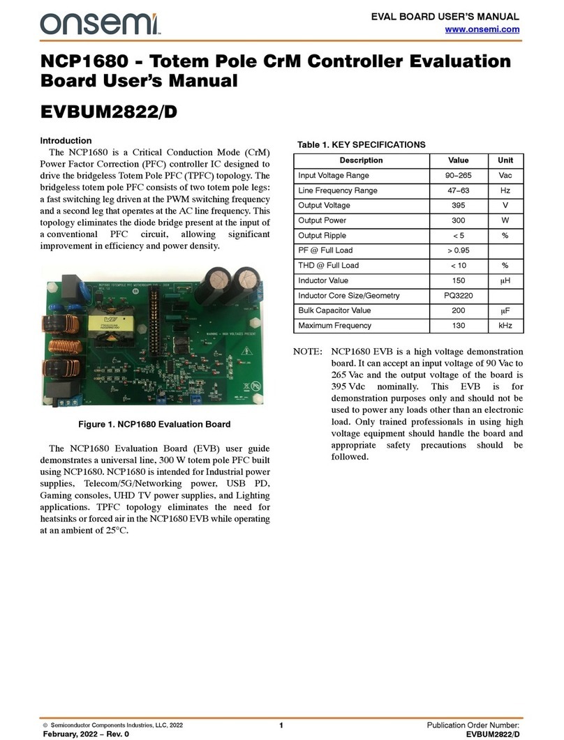
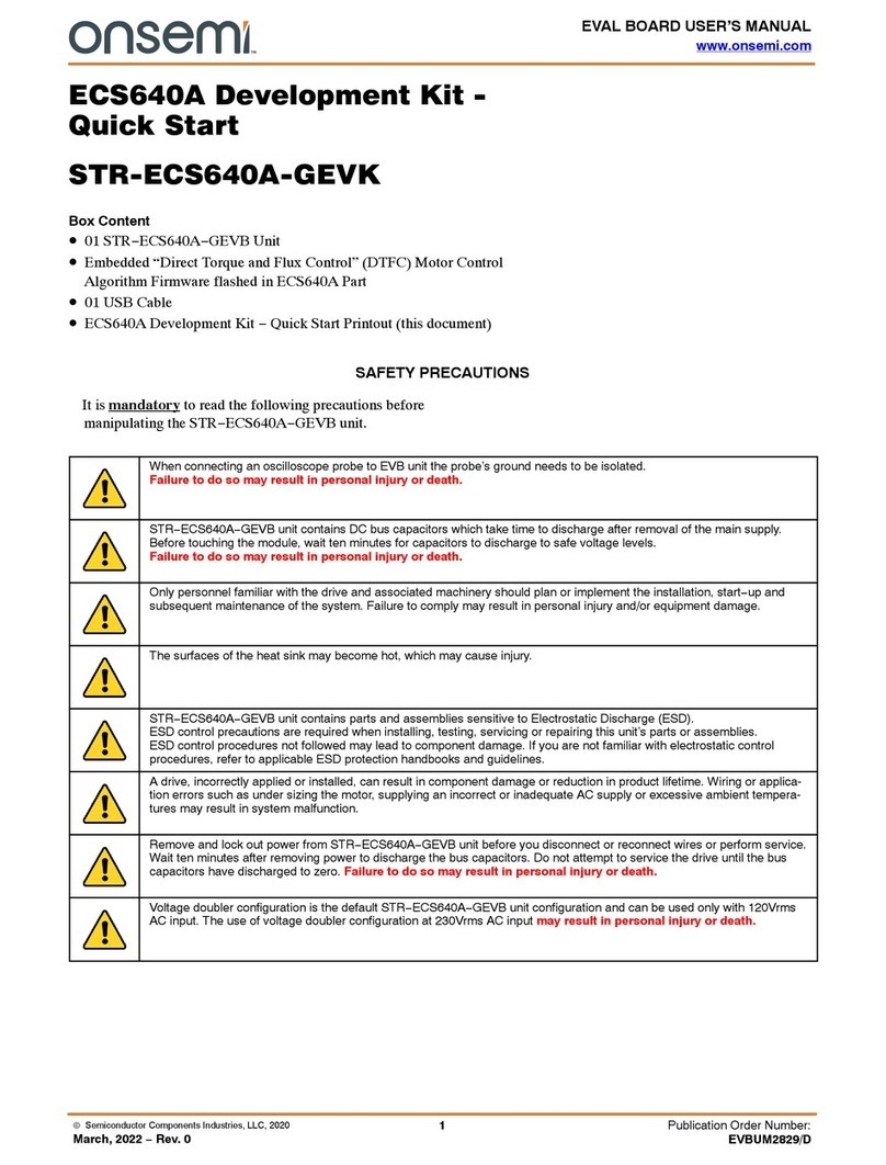
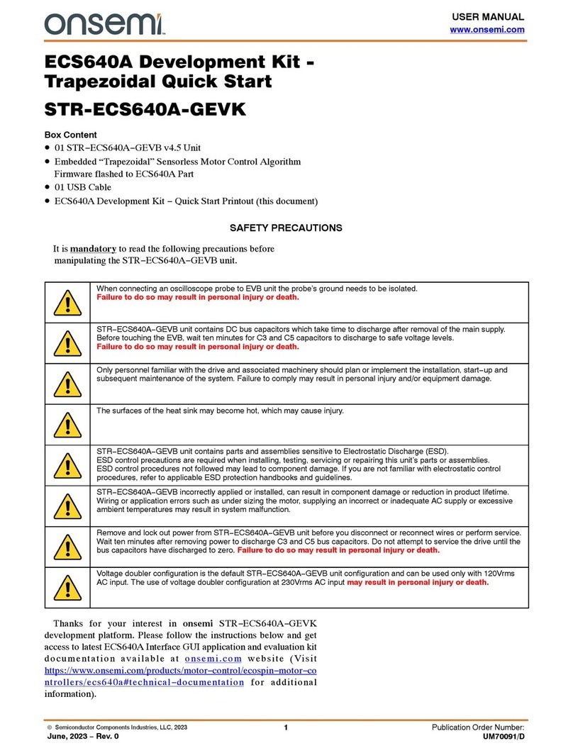
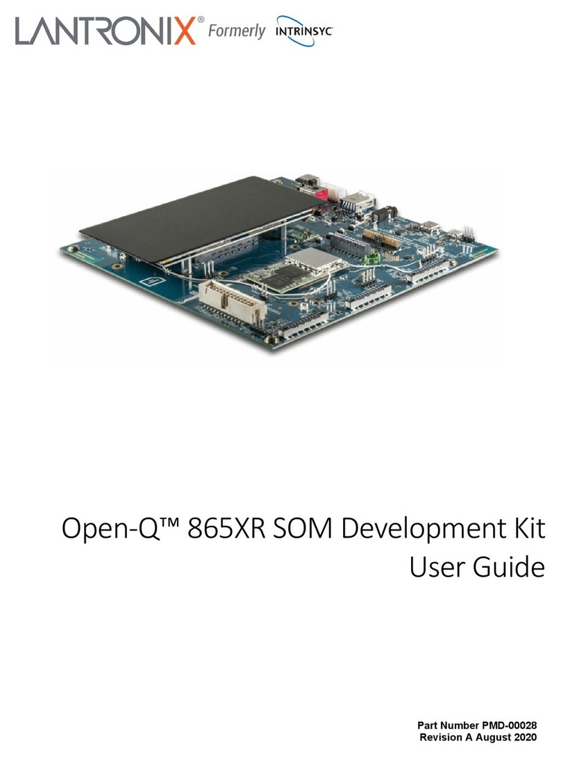
onsemi AXM0F343 User manual

www.onsemi.com
2
Table of Contents
1. Introduction................................................................................................ 3
2. Installation ................................................................................................. 4
3. Create a new Project................................................................................... 5
3.1. Import Eclipse Projects................................................................................... 5
3.2. Upgrading AXM0F343 CMSIS Pack ................................................................... 7
4. AX-ConfigurationUtility Main Panel ............................................................. 9
4.1. Wake on Radio Mode (WOR) ..........................................................................13
4.2. RX Synchronized with TX Mode.......................................................................15
5. Kit Configuration Panel ............................................................................. 18
6. Pin Configuration Panel............................................................................. 20
7. PHY Panel ................................................................................................. 21
8. Framing Panel........................................................................................... 24
9. Basic and Regulatory Tests Panel ............................................................. 28
10. Programming the Target boards ............................................................... 30
11. Comments on C-code Firmware ................................................................ 31
11.1. File Structure ...........................................................................................31
11.2. Define Statements for Tweaking the Firmware .............................................31
11.3. SYNC Packet RX Timing.............................................................................32
12. XTAL/TCXO Precision, Frequency Tracking and Bandwidth....................... 33
12.1. How to set up AFC range, FSK deviation and RX bandwidth ...........................33
Case 1: XTAL/TCXO precision, bitrate and carrier frequency are given .................33
Case 2: Bitrate and carrier frequency and FSK deviation are given ......................38
12.2. Background information ............................................................................40
13. Revision History........................................................................................ 42

AX-ConfigurationUtility User Manual
www.onsemi.com
3
1. Introduction
The AX-ConfigurationUtility is a hands-on configuration and firmware source code
generation tool for the AXM0F343.
It creates C-code firmware projects based on the AX-ConfigurationUtilityAPIManual
(described in DOCU/ AX-ConfigurationUtilityAPIManual.pdf), which demonstrate the use of
the AX5043 transceiver together with the AXM0F343 SoC for packet transmission and
reception in several modes.
Using the simple GUI, the transmitter (MASTER) and receiver (SLAVE) can be easily
configured into the desired mode. The generated Eclipse-compatible firmware can then be
imported within the ON Semiconductor IDE and flashed via the standard AXM0F343
toolchain.
Further modification of the generated firmware source code can be done directly using the
ON Semiconductor IDE. Additionally, the project can be at any time be reloaded into AX-
ConfigurationUtility, to automatically modify the desired wireless parameters.
This document first illustrates installation requirements and the steps needed to create a
new project within a GUI, and how to import it within the ON Semiconductor IDE.
Afterwards, each panel of the GUI is described in detail with explanations and hints on how
to build the desired radio firmware. Finally, a generic overview on the code and utilities is
given.

AX-ConfigurationUtility User Manual
www.onsemi.com
4
2. Installation
Hardware and requirements:
•64-bit Windows 7 or later
•at least 4GByte RAM
•1GB free hard disk space
•free USB port
Software requirements:
•Install the ON Semiconductor IDE and all sub-components. The IDE is used
to edit and flash the firmware.
•Install the AX-ConfigurationUtility. The GUI is used to generate custom
projects
•For AX-ConfigurationUtility to work correctly you need to import the ON
Semiconductor AXM0F343 CMSIS Pack within the ON Semiconductor IDE
first.
Additionally, you need to install the ARM.CMSIS.5.8.0 Pack downloadable
from https://github.com/ARM-software/CMSIS_5/releases/tag/5.8.0
•To verify and validate SoC AXM0F343, compiler such as ARM GCC (Version
5.0 and above) is required to be installed.
AX-ConfigurationUtility is included as a standalone installer. Please uninstall any previously
installed versions of this software before starting a new installation.
At the end of installation, a reboot may be requested; however, this is not mandatory.

AX-ConfigurationUtility User Manual
www.onsemi.com
5
3. Create a new Project
The AX-ConfigurationUtility GUI can be used to create projects for AXM0F343.
Open the AX-ConfigurationUtility.exe to create a new project as below:
•Device: This populates the devices supported in the current AX-ConfigurationUtility
GUI namely AXM0F343-64 and AXM0F343-256.
•Compiler: For either of the device the compiler supported is ARM-GNU-GCC.
•Debugger: JLINK (version 670e and above) is the only debug interface available
with the current AX-ConfigurationUtility GUI.
•Kit Types: This option is also populated based on the selected device
oFor AXM0F343-64
▪AXM0F343-64-868-1-GEVB
▪AXM0F343-64-915-1-GEVB
oFor AXM0F343-256
▪AXM0F343-256-868-1-GEVB
▪AXM0F343-256-915-1-GEVB
3.1. Import Eclipse Projects
The project created using AX-ConfigurationUtility consists of folder templatefirmware. This
directory consists of eclipse projects and template source code specific to AXM0F343-64
and AXM0F343-256 SoC.

AX-ConfigurationUtility User Manual
www.onsemi.com
6
Based on the Target board, the eclipse project can be imported relatively using
Projectdir\MASTER\axm0f343-64 or Projectdir\MASTER\axm0f343-256.Similar logic
applies to Slave/Tests.
Eclipse projects for various configurations can be opened as below: -
•Open Projects from File System using Eclipse IDE

AX-ConfigurationUtility User Manual
www.onsemi.com
7
•Open Eclipse Project
•Enable Message Box Popup in Eclipse if File got updated outside of Eclipse Editor:
Goto Window -> Preferences -> General -> Workspace and uncheck the
option "Refresh on access" in Eclipse.
•To debug the driver firmware in the library included in the pack, path to the
library source requires remapping as below
a. Goto Eclipse→Window→Preferences→C/C++→Debug→Source Lookup
Path→Add
b. Add Path mapping and enter the below item in the path mapping
c. C:\Users\fg8y4b\ON_Semiconductor\PACK on the LHS
d. C:\Users\ID\ON_Semiconductor\PACK →ID to be replaced with the User’s
ID where pack is installed in respective PC’s.
By doing the above steps, the firmware drivers source files within the F343
pack is available for debug.
3.2. Upgrading AXM0F343 CMSIS Pack
The Template firmware accesses CMSIS pack specific to the AXM0F343 SoC.
The Eclipse projects in Template firmware accesses the CMSIS pack drivers relatively be
defining environment variable in the project settings namely
AXM0F343_CMSIS_PACK_ROOT. Currently, this variable is set to a value
“${cmsis_pack_root} \ONSemiconductor\AXM0F343\1.4.0”
“1.4.0” denotes the PACK version that is configured. This needs to be updated to the
upgraded version as below. For example: if the pack version is upgraded to 1.5.0, it
should be modified in the eclipse project settings as below in the installation directory of

AX-ConfigurationUtility User Manual
www.onsemi.com
8
AX Configuration Utility located at C:\Program Files (x86)\ON Semiconductor\AX-ConfigurationUtility
in 6 different locations for debug and release configurations:-
e. Master
i. axm0f343-64
ii. axm0f343-256
f. Slave
i. axm0f343-64
ii. axm0f343-256
g. Tests
i. axm0f343-64
ii. axm0f343-256
The variable is defined in the environment section of the eclipse project in each of the
above 6 different sets in debug and release configurations. The Variable can be
accessed by navigating to Project→Properties→C/C++ Build →Environment

AX-ConfigurationUtility User Manual
www.onsemi.com
9
4. AX-ConfigurationUtility Main Panel
Start a new project using the Project menu. You must specify a project directory where
AX-ConfigurationUtility will create firmware projects called MASTER, SLAVE and TESTS. To
open an existing project, use the directory chooser dialog to descend into the project
directory (where the axradiolabstate.xml file resides) and hit done. Note: do not open the
template_firmware_504x project inside the AX-ConfigurationUtility installation directory,
as this is the template from which the firmware is copied upon creating a new project.
Follow through the main panel step-by-step to configure your project:
1. Select the TX operation mode:
•TX periodic (LPOSC): Periodic packet transmission driven by the MCUs low
power RC oscillator.
•TX periodic (LPXOSC): Periodic packet transmission driven by the MCU’s low
power 32kHz tuning fork crystal oscillator
1.
.
2.
4.
.
7.
.
.
5.
.
.
8.
.
.
3.
.
6.
.

AX-ConfigurationUtility User Manual
www.onsemi.com
10
•TX on demand: Packet transmission upon pressing a button.
2. Select the RX operation mode: RX Continuous (RX always on): Packet reception
keeping the receiver continuously on. This mode is used for AC-powered systems and
allows asynchronous packet reception with low latency.
•Wake on Radio: Packet reception with the receiver waking up periodically and
going immediately back to sleep if no signal is detected. The wake-up is driven
by the Radio’s low power RC oscillator and does not require any MCU activity.
The MCU is only woken up once a valid packet has been received. This mode is
well suited e.g. for infrequently operated remote-control applications and
achieves very low (idle) current consumption. Mind that preambles longer
than the time between RX wakeups are necessary. The latter also
determines the RX latency.
•RX Synchronized with TX: Periodic packet reception enabling the receiver
only for the time slots in which packets are expected. This is appropriate
whenever periodic data transmission is required. Timing is driven by the MCU’s
low power 32kHz tuning fork crystal oscillator and thus requires MCU activity.
It is mandatory to use TX periodic (LPXOSC) on the transmitter side.
•The Send acknowledge checkbox causes the slave module (“RX”) to answer
successful packet reception with an acknowledge packet. The master module
(“TX”) tries to receive the acknowledge packet. The smiley on the LCD/UART
print indicates whether the acknowledge packet has been received. Failure is
also signaled via LED1. Optionally the MASTER can retransmit a packet if
acknowledge fails. This feature is enabled by setting Max number of
retransmissions to a nonzero value. The acknowledge mode is the reason why
the terminology MASTER and SLAVE (rather than TX and RX) has been chosen.
The acknowledge feature can be selected in all TX and RX modes.
3. Buttons to open configuration panels for Kit Configuration, Pin Configuration, PHY layer
and Framing. The PHY panel covers physical parameters of the wireless link such as
carrier frequency, data rate and the modulation scheme. The Framing panel deals with
packet delimiting, CRC etc.
4. Calculate Registers calculates register values to configure the selected device/Radio
according to your Pin Configuration, PHY and Framing selections.
5. Save & Write Output:
The MASTER and SLAVE firmware projects are created in your project directory (if not
present yet) upon hitting the Save & Write Output button. Manual changes in the
firmware projects are never overwritten by the GUI except for the configuration files
in your_projectdir /AX_Radio_Lab_output/.
•Saves configuration and register values into
your_projectdir\axradiolabstate.xml, allowing you to reopen your project with
AX-ConfigurationUtility.
AX-ConfigurationUtility User Manual
www.onsemi.com
11
•Outputs files config.c, configmaster.[ch] and configslave.[ch] to
your_projectdir\AX_Radio_Lab_output\
These files are included by / linked to the MASTER, SLAVE and TESTS
firmware projects.
•The firmware projects MASTER and SLAVE are written into your project
directory if they are not present yet.
6. After calculating register values, you can optionally tweak values using Expert
Settings. Click values in the rightmost column of the Expert Settings panel to edit.
Tweaked values are sticky. They keep overriding the defaults even if the defaults have
changed (e.g. upon making changes in the PHY panel and hitting Calculate
Registers). Tweaked values are highlighted in yellow (or green if they accidentally
correspond to the default values). The changes active indicator in the main panel
reminds you that tweaked values are being used. Double click a tweaked register
(column 1, 2 or 3) to return to the default value. Hitting Reset Changes at the bottom
of the Expert Settings panel or clicking the changes active indicator in the main
panel drops all tweaks.
7. Opens the Basic & Regulatory Tests panel, allowing you to transmit CW, simple
patterns, or random data and to measure bit error rates.
8. Open Project Folder –This enables the user to open the project directory in the
explorer.

AX-ConfigurationUtility User Manual
www.onsemi.com
12
9. TX-RX Modes and timer usage
Mode, Purpose
Used timer
Radio / MCU activity1
TX periodic (LPOSC),
Periodic packet transmission
MCU CMSIS Pack based timer infrastructure
with timer0 clocked by MCU LPOSC (640hz RC
oscillator)
MCU periodically wakes up, powers up the
TX and initiates packet transmission
TX periodic (LPXOSC),
Periodic packet transmission
(used with RX Synchronized
with TX)
MCU CMSIS Pack based timer infrastructure
with timer0 clocked by MCU LPXOSC (32kHz
tuning fork crystal oscillator)
MCU periodically wakes up, powers up TX
and initiates packet transmission.
TX on demand,
Packet transmission upon
pressing a button or similar
event.
MCU CMSIS Pack based timer infrastructure
with timer0 clocked by MCU LPOSC (640hz RC
oscillator)
Only used for generating a timeout in ACK
mode
MCU wakes up upon pressing a button,
powers up the TX and initiates packet
transmission.
RX Continuous,
AC-powered systems
(allows asynchronous
packet reception)
MCU CMSIS Pack based timer infrastructure
with timer0 clocked by MCU LPOSC (640hz RC
oscillator)
Only used for ACK timing and channel state
polling.
RX is continuously on. Upon receiving a
valid packet, it generates an interrupt
waking up the MCU.
Wake on Radio,
Remote control
(asynchronous packet
reception at low idle
currents at the expense of
long preambles and
increased latency)
AX5043 LPOSC (640Hz RC oscillator) for
autonomous wake-up of the AX5043
MCU CMSIS Pack based timer infrastructure
with timer0 clocked by MCU LPOSC (640hz RC
oscillator)
Only used for generating a timeout in ACK
mode
RX periodically wakes up and checks for
signal. Upon receiving a valid packet, it
generates an interrupt waking up the MCU.
RX Synchronized with
TX,
Low power periodic data
transmission
MCU CMSIS Pack based timer infrastructure
with timer0 clocked by MCU LPXOSC (32kHz
tuning fork crystal oscillator)
MCU periodically wakes up, powers up the
RX and waits for packet reception or
timeout.
Table 1: Summary of TX and RX modes and corresponding firmware projects for AXM0F343 SoC
1
MCU activity apart from timekeeping wake-ups due to the running CMSIS pack-based timer infrastructure.

AX-ConfigurationUtility User Manual
www.onsemi.com
13
4.1. Wake on Radio Mode (WOR)
In Wake on Radio mode the receiver periodically wakes up and searches the channel for
a signal. In absence of signal the receiver is switched off again immediately to save power.
If a signal is detected the receiver stays on and looks for a valid packet delimiter. The
Radio performs this task autonomously. Only after a valid packet has been received and
is waiting in the FIFO, the Radio wakes up the micro controller via an interrupt. A typical
application of this mode would be an infrequently operated remote control. The “WOR
Settings” button opens the Wake on Radio panel:
Figure 1: Wake on Radio. WOR settings panel.
1. This field configures how often the receiver wakes up and checks for signal. Waking
up less often reduces the average RX (idle) current. However, it increases the
necessary preamble length and average latency since the preamble needs to be at
least as long as the gap between two successive wake ups.
2. The “enable RSSI threshold” option determines how the RX searches for signal upon
wake up:
a. If this option is disabled, the RX directly scans for preamble pattern.
Sensitivity in this mode is comparable to continuous RX operation.
b. If this option is enabled the RX first acquires an RSSI value. The scan for
preamble pattern is performed only if RF energy is detected. This reduces
current consumption (most notably at low data rates) since the RSSI
measurement is faster than the scan for preamble pattern. The drawback is
a reduction of sensitivity, since the RSSI threshold has to be set several dB
above the sensitivity limit to prevent false positives.
The RX proceeds to scanning for preamble if RSSI > absolute threshold AND
RSSI >= (background RSSI + relative threshold). Background RSSI is the
RSSI average over past wake ups.
1.
.
.
2.
.
.
3.
.
.

AX-ConfigurationUtility User Manual
www.onsemi.com
14
3. This field allows customization of the RSSI settling time. Longer settling times give
more stable RSSI measurements at the expense of higher current consumption.
Changes are written to the expert panel.
Make sure you understand the following points:
•An important part of the process of powering-up the receiver and deciding whether
a preamble signal is present takes a time inversely proportional to the data rate.
To achieve minimum current consumption, you should therefore use the maximum
possible data rate (100kbps). The time the receiver searches for a preamble signal
can be customized via the TMGRXPREAMBLE1 register in the expert panel.
•Frequency tracking (AFC) requires settling time, which adds to the receiver start-
up time and therefore increases the average current consumption. Large data rates
and precise frequency references render frequency tracking unnecessary.
•The average receiver (idle) current is proportional to the wake-up frequency. On
the other hand, in the remote control mentioned above, the wake-up frequency
determines how quickly the receiver will react.
•Mind that the current estimate displayed in the main panel is the idle current in
absence of a signal. Thus, while the RX wakes up periodically, actual packet
reception is the exception in this mode, occurring only e.g. if a remote-control
button was pressed. This is in contrast to the Synchronized with TX mode; in
which a packet is expected each time the RX wakes up.

AX-ConfigurationUtility User Manual
www.onsemi.com
15
4.2. RX Synchronized with TX Mode
The purpose of RX Synchronized with TX mode is periodic reception of packets with
minimal current consumption by enabling the RX only for the time slots in which packets
are expected. Short preambles can be used on the TX side
2
. The following points explain
how the RX Synchronized with TX mode works:
•RX Synchronized with TX mode is used together with TX periodic (LPXOSC)
on the TX side. Timing is driven by the MCU’s low power 32kHz tuning fork crystal
oscillator which ensures an accurate packet frequency and thus allows for tight
margins in the time slots in which the RX is enabled.
•After power up LPXOSC is settled and the RX is switched continuously on until a
packet is received, or a timeout occurs. LED1 indicates the RX is running. When a
packet is received the RX is put to sleep and only wakes up again for the time slot
in which the next packet is expected.
•With each further packet reception, the RX measures the effective time elapsed
since the last packet and (via low pass filtering) corrects its own wake-up frequency
accordingly. This corrects for crystal variations as well as temperature differences
and slow gradients and minimizes required margins in the RX-on time slots. (An
increased margin is used for the packet reception right after synchronization, where
the effective period has not been measured yet.)
•If no packet is received during an RX-on time slot, the RX margins are increased
for the next time slot. If no packet is received during N subsequent time slots, the
RX module switches back to synchronization mode, i.e. the RX is switched on
continuously until a packet is received or a timeout occurs. (This synchronization
mode is the same as for initial synchronization after power up. The only difference
lies in the timeout interval: A timeout (in seconds) can be configured for initial
synchronization after power-up (e.g. time to put batteries into the TX module). A
second timeout (in packet periods) applies for re-synchronization after losing
multiple packets in a row.
•If (re-)synchronization fails, (no packet is received until the timeout), the RX
module is put to sleep for a configurable, typically long, period before trying to
synchronize again. The rationale here is to limit RX power consumption in the case
where the TX is off or out of reach.
•The Sync Timing button opens the Sync Timing panel, where various timing
parameters can be configured.
2
This contrasts with the asynchronous nature of Wake on Radio mode, where a preamble is at least as long as
the RX sleep interval is required.

AX-ConfigurationUtility User Manual
www.onsemi.com
16
Figure 2: RX Synchronized with TX, Sync Timing panel for AXM0F343
1. Packet period (send packet every): This is simply a duplicate of the TX
periodic (every) field in the main panel for convenience.
2. Synchronization time-out after power-up: Time the RX tries to receive the first
packet, before temporarily giving up and switching to re-sync pause mode. E.g.
this is the time you have to put batteries into the TX module after powering up the
RX.
3. Re-Synchronization after N lost packets: Determines in how many subsequent
RX-on time slots packet reception can fail before the RX switches to back to
synchronization mode.
4. Re-synchronization time-out: Time the RX tries to receive a packet for (re-)
synchronization before temporarily giving up and switching to re-sync pause mode.
5. Re-synchronization pause (upon re-synchronization time-out): Time for
which the RX sleeps after failing to re-synchronize before trying again.
6. LPXOSC frequency: Frequency of the low power tuning fork crystal oscillator.
7. LPXOSC precision: Precision of the low power tuning fork crystal oscillator.
8. LPXOSC settling time (after power-up): TX as well as RX modules wait for this
time before transmitting / trying to receive packets. This is to prevent
synchronization and period measurement with an insufficiently settled clock source.
1.
.
2.
.
3.
.
4.
.
5.
.
6.
.
.
7.
.
.
8.
.
.
9.
.
10.
.
11.
.
.

AX-ConfigurationUtility User Manual
www.onsemi.com
17
9. Minimum RX margin: RX margin determines how long the RX is running before
the expected packet start. The same margin is also used as a timeout: The RX is
powered down if no frame delimiter is detected by the time it was expected plus
RX margin. (RX running means synthesizer running and analog baseband settled,
but no AGC, AFC and bit synchronization, since there is no signal yet.) The minimum
value specified here must accommodate timing fluctuations in normal operation. A
default value is computed from packet period and LPXOSC precision. Double
click the field to change it manually. If packet reception fails in a given RX-on time
slot, the firmware automatically increases the margin for the next time slot.
10. RX margin after re-synchronization: An increased RX margin which is used for
the RX-on time slot right after (re-) synchronization. This is necessary, since (re-)
synchronization only aligns the phases of periodic TX and RX. The RX needs a
further packet to measure and adjust the wake-up period. Therefore, the margin
of the first RX-on time slot has to be large enough for the full, uncorrected timing
deviation.
11. Radio XTAL prestart time: Determines how long the XTAL reference oscillator of
the radio chip is settled before the RX synthesizer is started.

AX-ConfigurationUtility User Manual
www.onsemi.com
18
5. Kit Configuration Panel
In the Kit Configuration panel displays the devices/compiler/debugger and the kit type as
chosen by the user while creating the radio configurator project.
Further, it allows the user to enable/disable debug prints, sleep options etc
The displayed device info is non-configurable and shows based on the user selection as
below.
Devices/MCUs:
oAXM0F343-64
oAXM0F343-256
Kit types based on the selected device:
oFor AXM0F343-64
▪AXM0F343-64-868-1-GEVB
▪AXM0F343-64-915-1-GEVB
oFor AXM0F343-256
▪AXM0F343-256-868-1-GEVB
▪AXM0F343-256-915-1-GEVB
The kit configuration panel consists of device, compiler, debugger, and kit type. This
panel displays the devices, kit types, compilers and debuggers as selected by the User
for reference. Enable/Disable debug print, Sleep options etc could be selected/deselected
by the user.
Figure 3: Kit Configuration panel for AXM0F343
Output Debug Info: For AXM0F343, the debug messages are transmitted to a serial
terminal via UART0. This option enables to print debug information. The terminal settings
should be configured to set baud rate = 115200, stop = 1, parity none, data = 8 bits.

AX-ConfigurationUtility User Manual
www.onsemi.com
19
Extra debug messages on debug window: This option produces extra information
about the status change of the radio state.
Use MCU hibernate instead of sleep option decides if the MCU uses hibernate mode
instead sleep mode. When hibernate mode is enabled in the kit configuration panel, after
programming the device with the generated firmware, jumper J10 should be removed and
hard reset should be done for the hibernate mode to work.

AX-ConfigurationUtility User Manual
www.onsemi.com
20
6. Pin Configuration Panel
Figure 4: Pin Configuration panel for AXM0F343
•VCO Cal Config: VCO calibration is enabled by default
•Ref Osc Config: select XTAL or TCXO
•PA Config: select differential, single ended or both power amplifier(s)
•Loop Filter Config: determines whether the internal or an external PLL loop filter is
used.
•VCO Config: Select VCO 1 (fully integrated VCO with on-chip inductor), VCO 2
(using an external inductor), or an entirely external VCO
•SYS CLK config: default selected as 1
•IRQ Config: Output IRQ. No other setting is sensible if the AX5043 module is
connected to the main board.
Table of contents
Other onsemi Microcontroller manuals