OSD Audio OSD024T1983-38 User manual
OSD DISPLAYS
12124 High Tech Av. Ste. 100
Orlando, FL 32817
Phone: 407-629-0500
Fax: 407-645-5376
www.osddisplays.com
Customer:
Model Number: OSD024T1983-38
Specification Number:
Date: 09/09/2010
Version: 1.1
For Customer’s Acceptance
Approved by Comments
Approved by Reviewed by Prepared by
P.2
REVISIONRECORD
REVNO. REVDATE CONTENTS REMARKS
0.1 2009-12-23 Firstrelease Preliminary
1.0 2010-1-13 Fullspec /
1.1 2010-9-9 Updatethedrawing P.5

P.3
CONTENTS
GENERALINFORMATION
EXTERNALDIMENSIONS
ABSOLUTEMAXIMUM RATINGS
ELECTRICALCHARACTERISTICS
BACKLIGHTCHARACTERISTICS
ELECTRO-OPTICALCHARACTERISTICS
INTERFACEDESCRIPTION
REFERENCE APPLICATIONCIRCUIT
RELIABILITY TESTCONDITIONS
INSPECTIONCRITERION
PRECAUTIONSFORUSINGLCDMODULES
PACKINGSPECIFICATION
PRIOR CONSULTMATTER
FACTORY CONTACTINFORMATION
WRITTENBY CHECKEDBY APPROVEDBY
HUANGYANXUE ZHAO ZHIWEI ZHANG SHUHANG
P.4
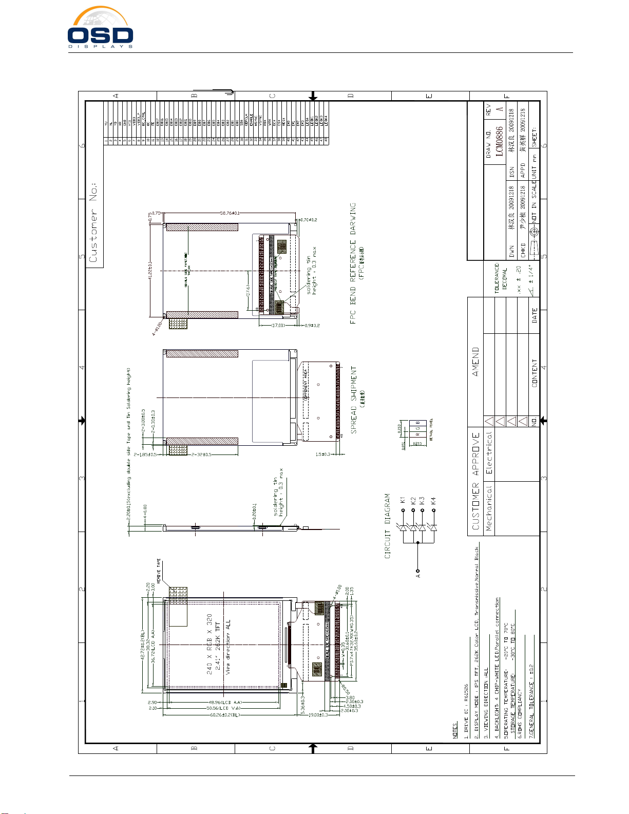
nGENERALINFORMATION
ItemContents Unit
LCDtype TFT/TRANSMISSIVE /
Viewing direction Fullviewingangle O Clock
Modulearea(W ´H ´T) 42.72×60.26×2.20 mm3
Viewing area(W´H) 38.32×50.56 mm2
Activearea(W´H) 36.72×48.96 mm2
NumberofDots 240RGB×320 /
Pixelpitch(W ´H) 0.153×0.153 mm2
DriverIC R61526 /
InterfaceType MPU/SPI+RGB /
Inputvoltage 2.8 V
ModulePowerconsumption 279 mw
Colors 262K /
BacklightType LED /
P.5
nEXTERNALDIMENSIONS
1/1
K4
K3
K2
K1
A
K4
K3
K2
K1
A
P.6
nABSOLUTEMAXIMUM RATINGS
Parameter Symbol Min Max Unit
Supplyvoltageforlogic VDD3/VCI -0.3 4.6 V
InputvoltageVIN -0.3 VDD3+0.3 V
Operating temperatureTop -20 70 °C
StoragetemperatureTST -30 80 °C
HumidityRH - 90%(Max60 °C) RH
nELECTRICALCHARACTERISTICS
DC CHARACTERISTICS
ParameterSymbol Min Typ Max Unit
Supplyvoltageforlogic VCI 2.5 2.8 3.3 V
I/O powersupply VDD3 1.65 1.8/2.8 3.3 V
InputCurrent Idd - 10.03 20.06 mA
Inputvoltage'H'level VIH 0.8VDD3 - VDD3 V
Inputvoltage'L'level VIL 0 - 0.2VDD3
V
Outputvoltage'H'level VOH 0.8VDD3 - - V
Outputvoltage'L'level VOL - - 0.2VDD3
V
nBACKLIGHTCHARACTERISTICS
ItemSymbol Min.
Typ. Max. Unit Condition
ForwardvoltageVf 2.9 3.1 3.4 V
LuminanceLv 39004300 4700 cd/m2
If=72mA
Ta=25℃
NumberofLED- - 4 - Piece -
ConnectionmodeP - Parallel
- - -
Using condition:constantcurrentdrivingmethodIf=72mA(+/-10%).
P.7
nELECTRO-OPTICALCHARACTERISTICS
ItemSymbol Condition Min Typ Max Unit
Remark
Note
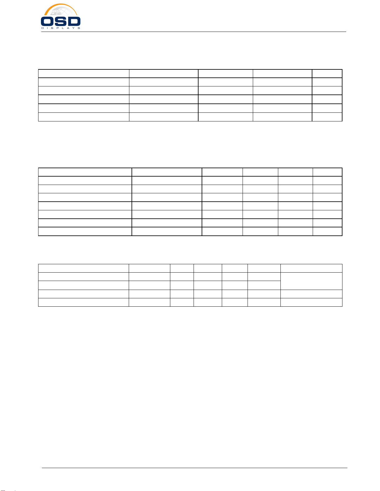
Responsetime
Tr+Tf - 26 39 ms Fig.1 4
Contrastratio
Cr 300 842 - --- FIG2. 1
Luminance
uniformitydWHITE 85 94 - % FIG2. 3
Surface
LuminanceLv
θ=0°
Æ=0°
Ta=25
209 261 - cd/m2
FIG2. 2
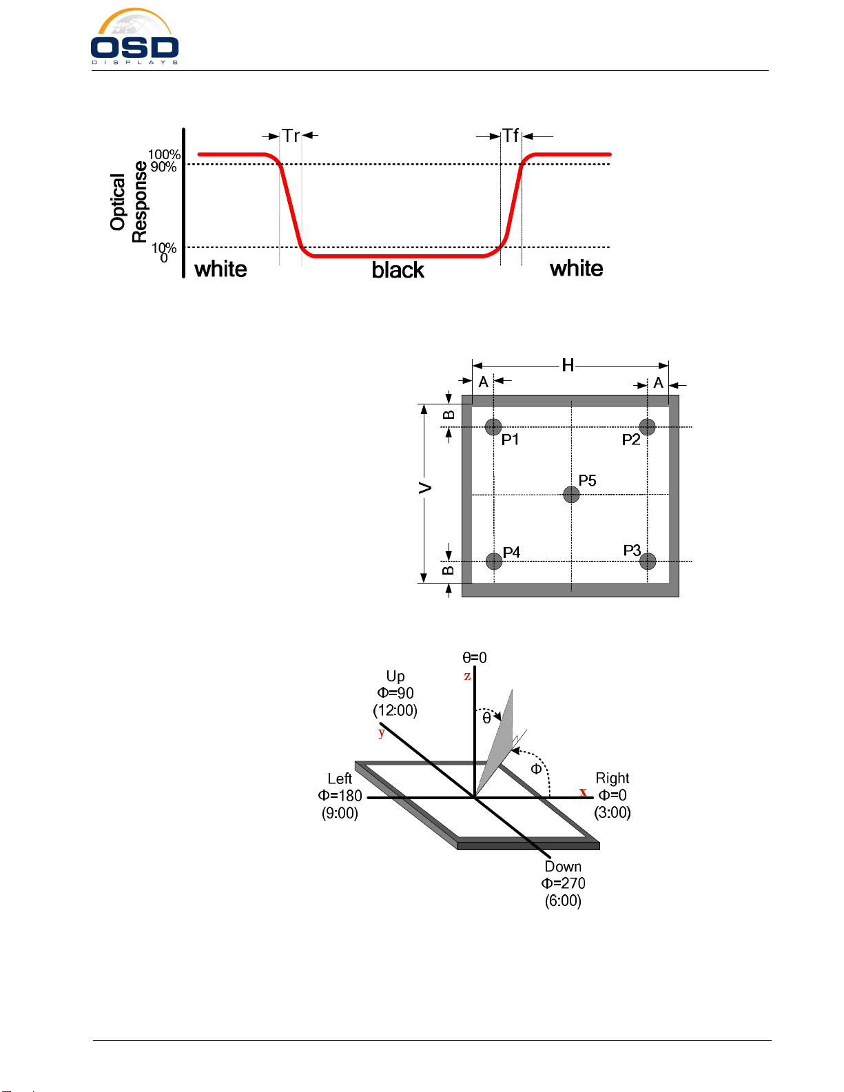
Æ=90°70 80 - deg FIG3.
Æ=270°70 80 - deg FIG3.
Æ=0°70 80 - deg FIG3.
Viewing angle
rangeq
Æ=180°70 80 - deg FIG3.
6
Redx 0.5918
0.6418
0.6918
-
Redy 0.2804
0.3304
0.3804
-
Greenx 0.2555
0.3055
0.3555
-
Greeny 0.5186
0.5686
0.6186
-
Bluex 0.0930
0.1430
0.1930
-
Bluey --- 0.0382
0.0882
-
Whitex 0.2207
0.2807
0.3407
-
CIE(x,y)
chromaticity
Whitey
θ=0°
Æ=0°
Ta=25℃
0.2288
0.2888
0.3488
-
FIG2. 5
Note1. ContrastRatio(CR)isdefinedmathematicallybythefollowingformula.Formore
informationseeFIG2.:
(
)
( )
AverageSurface Luminance with all white
pixels P1,P2,P3,P4,P5
ContrastRatio = AverageSurfaceLuminance withall black
pixelsP1,P2,P3,P4,P5
Note2. SurfaceluminanceistheLCDsurface from thesurfacewithallpixelsdisplaying white.
FormoreinformationseeFIG2.
Lv=AverageSurfaceLuminancewithallwhitepixels(P1,P2, P3,P4,P5)
Note3. Theuniformityinsurfaceluminance(dWHITE)isdeterminedbymeasuringluminanceat
eachtestposition1through5,andthendividing themaximumluminanceof5pointsluminanceby
minimumluminanceof5pointsluminance.Formoreinformationsee FIG2.
,
,
SurfaceLuminancewithallwhitepixels
(,,,)
WHITE= MaxiSurfaceLuminancewithallwhitepix
els(,,,)
d
12345
12345
MinimumPPPPP
mumPPPPP
Note4. ResponsetimeisthetimerequiredforthedisplaytotransitionfromWhitetoblack(Rise
Time,Tr) andfromblacktowhite(DecayTime,Tf).ForadditionalinformationseeFIG1..
Note5. CIE(x,y)chromaticity,Thex,yvalueisdeterminedbyscreenactiveareaposition5.For
moreinformationseeFIG2.
Note6. Viewingangleistheangleatwhichthecontrastratioisgreaterthan2.ForTFTmodulethe
conrastratioisgreaterthan10.Theanglesaredeterminedforthehorizontalorxaxisandthe
verticaloryaxiswithrespecttothezaxiswhichisnormaltotheLCDsurface.Formore
informationseeFIG3.
Note7. ForViewingangleandresponsetimetesting,thetestingdataisbaseonAutronic-Melchers s
ConoScope.SeriesInstruments.Forcontrastratio,Surface Luminance,Luminanceuniformityand
CIE,thetestingdataisbaseonTOPCON sBM-5photodetector.
Note8. ForTFT module, Grayscalereverseoccursinthedirectionofpanelviewing angle
P.8
FIG.1. ThedefinitionofResponseTime
FIG.2. MeasuringmethodforContrastratio,surfaceluminance, Luminanceuniformity,CIE (x,
y)chromaticity
FIG.3. Thedefinitionofviewingangle
A:5mm
B:5mm
H,V:ActiveArea
Lightspotsize Æ=5mm, 500mm distance fromthe
LCDsurface todetectorlens
measurementinstrumentisTOPCON sluminance
meterBM-5

P.9
nINTERFACEDESCRIPTION
Pin
NO.
Symbol I/Oor
connectto Description Whennot
inuse
1 YU NC NC -
2 XL NC NC -
3 YD NC NC -
4 XR NC NC -
5 GND Powersupply Ground -
6 VCI Powersupply Powersupplyforliquidcrystalanalogcircuit.
AMP:2.5V~3.3V,TYPE:2.8V -
7 VDD3 Powersupply Powersupplytointerface pinsandthelogic.
AMP:1.65V~3.3V,TYPE:2.8V -
8 VDD3_P Powersupply
PowersupplytoLEDPWM.
Supplyavoltageaccording toLEDdriverinput.
ThisshouldbeconnectedtoVDD3evenwhen
LEDPWM isnotused.
VDD3
9 BC_CTRL
10 BC
O
ThesepinsareLEDPWMforthismodule.Control
signalforbrightnessofLEDbacklight.PWM
signal swidthisselectedfrom 256 values
between0%(Low)and100%(High)byVDD3_P
amplitude.LEDPWMcanbeusedasasignalto
turnLEDon/offwhenthebacklightcontrol
functionisnotused.
Open
11 TE O
Hostprocessor
TearingEffectoutputsignal.Leaveopenwhen
notused. Open
12~
29 DB[17:0] I/O
Hostprocessor
18-bitbi-directionaldatabusinDBITypeB
operation.
8-bitinterface:UseDB[7:0]
9-bitinterface:UseDB[8:0]
16-bitinterface:UseDB[15:0]
18-bitinterface:UseDB[17:0]
Abnormalcurrent(throughcurrent)isnot
conductedwhenCSXisHigh andthedatabusis
Hi-z.
18-bitinputdatabusinDPIoperation.
16-bitinterface:UseDB[15:0]
18-bitinterface:UseDB[17:0]
VDD3
orGND
orOPEN
30 SDA I/O
Hostprocessor
Serialdatainput/outputpininDBITypeC
operation.Dataisinputontherisingedgeof
signalSCL. Dataisoutputonthefallingedgeof
SCLwhenserialdataoutputpinisselected.
VDD3or
GND
31 DOTCLK I
Hostprocessor
Pixelclocksignal.Thedatainputtiming isseton
therisingedge.LeaveopenwhenDPIisnot
selected.Connecttohostprocessorandinputan
IOVCC1/GND signalalwayswhenDPIis
selected.
VDD3or
GND
32 ENABLE I
Hostprocessor
DataenablesignalinDPIoperation.
Low:Select(Accessible)
High:Notselect(Inaccessible)Leaveopenwhen
DPIisnotselected.Connecttohostprocessorand
inputanIOVCC1/GND signalalwayswhenDPI
isselected.
VDD3or
GND

p,
P.10
33 HSYNC I
Hostprocessor
Linesynchronoussignal. Lowactive.
LeaveopenwhenDPIIsnotselected.
Connecttohostprocessorandinputan
IOVCC1/GND signalalwayswhenDPIis
selected.
VDD3or
GND
34 VSYNC I
Hostprocessor
Framesynchronoussignal. Lowactive.
LeaveopenwhenDPIisnotselected.
Connecttohostprocessorandinputan
IOVCC1/GND
signalalwayswhenDPIisselected.
VDD3or
GND
35 RDX I
Hostprocessor
Readstrobesignal.DataarereadwhenRDXis
low. VDD3
36 WRX I
Hostprocessor
WritestrobesignalinDBITypeBoperation.
DataarewrittenwhenWRXisLow.
SynchronousclocksignalinDBITypeC
operation.
-
37 DCX I
Hostprocessor
Command/dataselectsignal
Low:Command
High:Data
Command/dataselectsignalinDBITypeC
operation(Option3).
-
38 CSX I
Hostprocessor
Systembusselectsignal.
Low:Select(Accessible)High:Notselect
(Inaccessible)
Makesuretoconnecttohostprocessor.Follow
ACtiming
tocontrolthesignal.ChipenablesignalinDBI
TypeCoperation(Option3).
-
39 RESX
I
HostProcessor
orexternalRC
oscillator
Resetpin.TheModuleisinitializedwhenRESX
isLow.Makesuretoexecutepower-onresetwhen
turning thepowersupplyon.
-
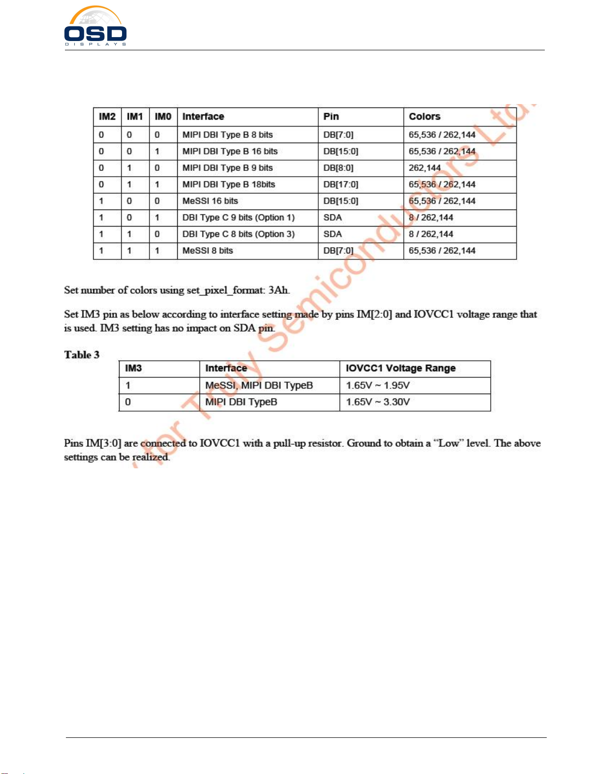
40 IM0 -
41 IM1 -
42 IM2 -
43 IM3
I
Hostprocessor
Interfaceselectingsignal.UsedtoswitchDBI
TypeB(18/16/9/8bits)andTypeC
(Option1/Option3).
Internallyconnectedtoapull-up resistor.Ground
ifnecessary.Forthedetails,pleasereferto
NOTE1.
-
44 LEDA LEDdriver LEDANODE -
45 LEDK1 LEDdriver LEDK1(CATHODE ) -
46 LEDK2 LEDdriver LEDK2(CATHODE ) -
47 LEDK3 LEDdriver LEDK3(CATHODE ) -
48 LEDK4 LEDdriver LEDK4(CATHODE ) -
P.11
Note1
nREFERENCEAPPLICATIONCIRCUIT
Pleaseconsult ourtechnicaldepartmentfordetailinformation.

P.12
nRELIABILITYTESTCONDITIONS
No. TestItem TestCondition Inspectionafter test
1 HighTemperatureStorage80±2℃/200hours
2 LowTemperatureStorage-30±2℃/200hours
3 HighTemperatureOperating
70±2℃/120hours
4 LowTemperatureOperating
-20±2℃/120hours
5 TemperatureCycle-20±2℃~25~70±2℃×10cycles
(30min.)(5min.)(30min.)
6 DampProofTest50℃±5℃×90%RH/120hours
7 VibrationTest
Frequency:10Hz~55Hz~10Hz
Amplitude:1.5mm,X,Y,Zdirection
fortotal3hours(Packing condition)
8 Dropping test
Droptothegroundfrom1mheight,
onetime,everysideofcarton.
(Packingcondition)
9 ESDtestVoltage:±8KVR:330ΩC:150pF
Airdischarge, 10time
Inspectionafter
2~4hoursstorageat
roomtemperature, the
sampleshallbefreefrom
defects:
1.AirbubbleintheLCD;
2.Sealleak;
3.Non-display;
4.missingsegments;
5.Glasscrack;
6.CurrentIddistwice
higherthaninitialvalue.
Remark:
1.Thetestsamplesshouldbeappliedtoonlyonetestitem.
2.Samplesizeforeachtestitemis5~10pcs.
3.ForDampProofTest,Purewater(Resistance>10MΩ)shouldbeused.
4.IncaseofmalfunctiondefectcausedbyESDdamage,ifitwouldberecoveredtonormalstateafter
resetting, itwouldbejudgedasagoodpart.
5.ELevaluationshouldbeexceptedfromreliabilitytestwithhumidityandtemperature:Somedefects
suchasblackspot/blemishcanhappenbynaturalchemicalreactionwithhumidityandFluorescence EL
has.
6.FailureJudgmentCriterion:BasicSpecification,ElectricalCharacteristic,MechanicalCharacteristic,
OpticalCharacteristic.
P.13
nINSPECTIONCRITERION
OUTGOING QUALITYSTANDARD PAGE1OF4
TITLE:FUNCTIONALTEST&INSPECTION CRITERIA MDSProduct
Thisspecificationismadetobeusedasthestandardacceptance/rejectioncriteriaforColormobile
phoneLCM.
1Sampleplan
SamplingplanaccordingtoGB/T2828.1-2003/ISO2859-1:1999andANSI/ASQCZ1.4-1993,
normallevel2andbasedon:
Majordefect:AQL0.65
Minordefect:AQL1.5
2. Inspectioncondition
Viewing distanceforcosmeticinspectionisabout30cmwithbareeyes,andunderan
environmentof20~40Wlightintensity,alldirectionsforinspecting thesampleshouldbewithin
45°againstperpendicularline.
3.DefinitionofinspectionzoneinLCD.
ZoneA:character/Digitarea
ZoneB:viewing areaexceptZoneA(ZoneA+ZoneB=minimumViewing area)
ZoneC:Outsideviewing area (invisibleareaafterassemblyincustomer sproduct)
Fig.1InspectionzonesinanLCD.
Note:Asageneralrule,visualdefectsinZoneCarepermissible, whenitisnotroublefor
qualityandassemblyofcustomer sproduct.
C
B
A

P.14
OUTGOING QUALITYSTANDARD PAGE2OF4
TITLE:FUNCTIONALTEST&INSPECTION CRITERIA MDSProduct
4.Inspectionstandards
4.1MajorDefect
Item
No
Itemstobe
inspected InspectionStandard Classification
ofdefects
4.1.1
All
functional
defects
1)Nodisplay
2)Displayabnormally
3)Missingvertical,horizontalsegment
4)Shortcircuit
5)Back-lightno lighting,flickering and abnormallighting.
4.1.2Missing Missingcomponent
4.1.3
Outline
dimension
Overalloutlinedimensionbeyondthedrawing isnotallowed.
Major
4.2CosmeticDefect
Item
No
Itemstobe
inspected InspectionStandard Classification of
defects
Fordark/whitespot, sizeΦis definedy
as Φ=
2
)( yx +x
1.
AcceptableQty
Zone
Size(mm) A B C
Φ≤0.10 Ignore
0.10<Φ≤0.15 2
0.15<Φ≤0.20 1
Clear
Spots
Blackand
whiteSpot
defect
Pinhole,
Foreign
Particle,
Dirtunder
polarizer
Φ>0.20 0
Ignore
Minor
4.2.1
DimSpots
Circle
shapedand
dimedged
defects
2.
AcceptableQty2. Zone
Size(mm) A B C
Φ≤0.2 Ignore
0.20<Φ≤0.40 3
0.40<Φ≤0.60 2
0.60<Φ≤0.80 1
Ignore
0.80<Φ0
Minor
P.15
OUTGOING QUALITYSTANDARD PAGE3OF4
TITLE:FUNCTIONALTEST&INSPECTION CRITERIA MDSProduct
4.2. CosmeticDefect
Item
No
Items tobe
inspected Inspection Standard Classification
ofdefects
Size(mm) AcceptableQty
Zone
L(Length) W(Width) A B C
Ignore W≤0.02 Ignore
L≤3.0 0.02<W≤0.03 2
L≤2.0 0.03<W≤0.05 1
0.05<W Defineas spot
defect
Ignore
4.2.2
Linedefect
Blackline,
Whiteline,
Foreign
material
under
polarizer,
Minor
4.2.3
Polarizer
scratch
If thePolarizerscratchcanbeseenaftermobilephone
coverassembling orintheoperatingcondition,judgeby
thelinedefectof4.2.2.
If thePolarizerscratchcanbeseenonlyinnon-operating
conditionorsomespecialangle, judgebythefollowing.
Size(mm) AcceptableQty
Zone
L(Length) W(Width)
A B C
Ignore W≤0.03 Ignore
5.0<L≤10.0
0.03<W≤0.05 2
L≤5.0 0.05<W≤0.08 1
0.08<W 0
Ignore
Minor
4.2.4
Polarize
Airbubble
Airbubbles betweenglass &polarizer
AcceptableQty2.Zone
Size(mm) A B C
Φ≤0.2 Ignore
0.20<Φ≤0.30 2
0.30<Φ≤0.50 1
0.50<Φ0
Ignore
Minor
P.16
OUTGOING QUALITYSTANDARD PAGE4OF4
TITLE:FUNCTIONALTEST&INSPECTION CRITERIA MDSProduct
4.3. CosmeticDefect
Item
No
Itemstobe
inspected InspectionStandard Classificationof
defects
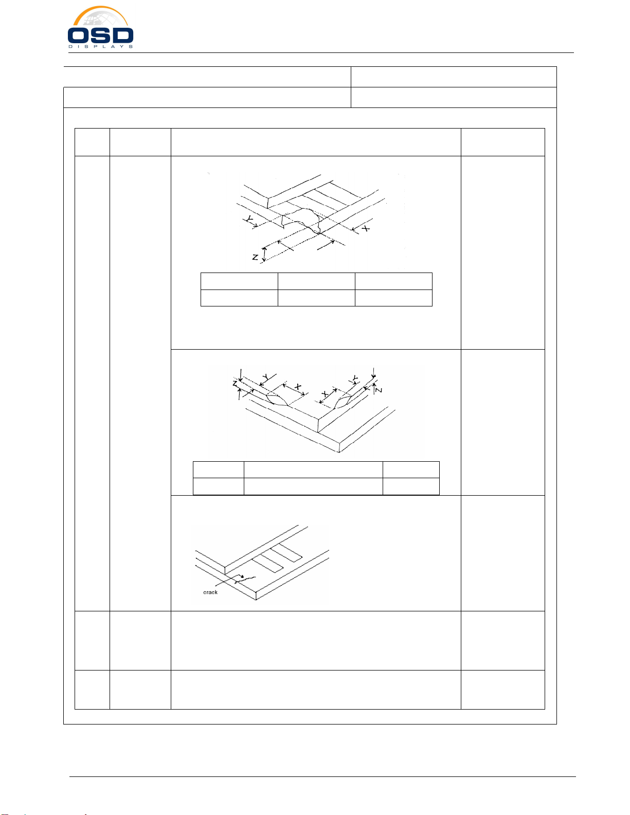
(i)Chips on corner
Notes:S=contactpadlength
Chipson thecornerofterminalshall notbeallowedtoextend
intotheITOpadorexposeperimeterseal.
X Y Z
≤2.0 ≤S Disregard
Minor
(ii)Usualsurfacecracks
X Y Z
≤3.0 <Innerborderlineoftheseal Disregard
Minor
4.3.5
Glass
defect
(iii)Crack
Crackstend tobreakarenotallowed.
Major
4.3.6
Parts
alignment
1) NotallowICand FPC/heat-sealleadwidthismorethan50%
beyondleadpattern.
2)Notallowchiporsoldercomponentisoff centermorethan
50% ofthepadoutline.
Minor
4.3.7
SMT
According tothe<Acceptabilityofelectronicassemblies>
IPC-A-610Cclass 2standard.Componentmissingorfunction
defectareMajordefect, theothersareMinordefect.
P.17
nPRECAUTIONSFORUSINGLCDMODULES
1HandingPrecautions
1.1 Thedisplaypanelismadeofglassandpolarizer.Asglass isfragile.Ittendstobecomeor
chippedduring handling especiallyontheedges.Pleaseavoiddroppingorjarring.Donot
subjectittoamechanicalshockbydropping itorimpact.
1.2 Ifthedisplaypanelisdamagedandtheliquidcrystalsubstanceleaksout,besurenottogetany
inyourmouth.If thesubstancecontactsyourskinorclothes,washitoffusing soapandwater.
1.3 Donotapplyexcessiveforcetothedisplaysurfaceortheadjoiningareassincethismaycause
thecolortonetovary.Donottouchthedisplaywithbarehands.Thiswill stainthedisplayarea
anddegradedinsulationbetweenterminals(somecosmeticsaredeterminedtothepolarizer).
1.4 Thepolarizercoveringthedisplaysurface oftheLCDmoduleissoftandeasilyscratched.
Handlethispolarizercarefully.Donottouch, pushorrubtheexposedpolarizerswithanything
harderthananHBpencillead(glass,tweezers,etc.).Donotputorattachanythingonthe
displayareatoavoidleavingmarksonit.Condensationonthesurfaceandcontactwith
terminalsduetocoldwilldamage,stainordirtythepolarizer.Afterproductsaretestedatlow
temperaturetheymustbewarmedupinacontainerbeforecoming intocontactwithroom
temperatureair.
1.5 Ifthedisplaysurface becomescontaminated,breatheonthesurfaceandgentlywipeitwitha
softdrycloth. If itisheavilycontaminated,moistenclothwithoneofthefollowingsolvents
-Isopropylalcohol
-Ethylalcohol
Donotscrubhardtoavoiddamagingthedisplaysurface.
1.6 Solventsotherthanthoseabove-mentionedmaydamagethepolarizer.Especially,donotuse
thefollowing.
-Water
-Ketone
-Aromaticsolvents
Wipeoffsalivaorwaterdropsimmediately,contactwithwateroveralongperiodoftime
maycausedeformationorcolorfading.Avoidcontactwithoilandfats.
1.7 Exercisecaretominimizecorrosionoftheelectrode.Corrosionoftheelectrodesisaccelerated
bywaterdroplets, moisturecondensationoracurrentflowinahigh-humidityenvironment.
1.8 InstalltheLCDModulebyusing themounting holes.WhenmountingtheLCDmodulemake
sureitisfree oftwisting,warpinganddistortion.Inparticular,donotforciblypull orbendthe
I/Ocableorthebacklightcable.
1.9 Donotattempttodisassembleorprocess theLCDmodule.
1.10 NCterminalshouldbeopen. Donotconnectanything.
1.11 Ifthelogiccircuitpowerisoff, donotapplytheinputsignals.
1.12 Electro-StaticDischargeControl,SincethismoduleusesaCMOSLSI,thesamecareful
attentionshouldbepaidtoelectrostaticdischargeasforanordinaryCMOSIC.Toprevent
destructionoftheelementsbystaticelectricity,becarefultomaintainanoptimum work
environment.
-BeforeremovingLCMfromitspackingcaseorincorporating itintoaset,besure
themoduleandyourbodyhavethesameelectricpotential. Besuretogroundthebodywhen
handling theLCDmodules.
-Toolsrequiredforassembling, suchassoldering irons,mustbeproperlygrounded.
MakecertaintheACpowersource forthesoldering irondoesnotleak.Whenusingan
electricscrewdrivertoattachLCM,thescrewdrivershouldbeofgroundpotentialityto
minimize asmuchaspossibleanytransmissionofelectromagneticwavesproducedsparks
comingfromthecommutatorofthemotor.
-Toreducetheamountofstaticelectricitygenerated,donotconductassembling

P.18
andotherworkunderdryconditions.Toreducethegenerationofstaticelectricitybecareful
thattheairintheworkisnottoodry.Arelativehumidityof50%-60%isrecommended.As
faraspossiblemaketheelectricpotentialofyourworkclothesandthatoftheworkbench
thegroundpotential.
-TheLCDmoduleiscoatedwithafilmtoprotectthedisplaysurface. Exercisecare
whenpeeling offthisprotectivefilmsincestaticelectricitymaybegenerated.
1.13 SinceLCMhasbeenassembledandadjustedwithahigh degree ofprecision,avoidapplying
excessiveshockstothemoduleormaking anyalterationsormodificationstoit.
-Donotalter, modifyorchangetheshapeofthetabonthemetalframe.
-Donotmakeextraholesontheprintedcircuitboard,modifyitsshapeorchangethe
positionsofcomponentstobeattached.
-Donotdamageormodifythepatternwritingontheprintedcircuitboard.
-Absolutelydonotmodifythezebrarubberstrip(conductiverubber)orheatseal
connector.
-Exceptforsolderingtheinterface,donotmakeanyalterationsormodificationswitha
soldering iron.
-Donotdrop,bend ortwisttheLCM.

P.19
2HandlingprecautionforLCM
2.1 LCMiseasytobedamaged.Pleasenotebelowandbecarefulforhandling.
2.2 Correcthandling:
2.3 Incorrecthandling:
Asabove picture, please handlewithanti
-
stati
cglovesaroundLCMedges.
Pleasedon tholdthe surface ofpanel.
Pleasedon ttouchICdirectly.
Pleasedon tstackLCM.
Pleasedon toperatewithsharpsticksuchas
pens.
Pleasedon tstretchinterfaceofoutput,such
asFPCcable.
Pleasedon tholdthe surface ofIC.
P.20
3StoragePrecautions
3.1 WhenstoringtheLCDmodules,thefollowing precautionarenecessary.
3.1.1 Storetheminasealedpolyethylenebag.If properlysealed,thereisnoneedforthe
desiccant.
3.1.2 Storetheminadarkplace.Donotexposetosunlightorfluorescentlight,keepthe
temperaturebetween0°Cand35°C,andkeeptherelativehumiditybetween40%RHand
60%RH.
3.1.3 Thepolarizersurface shouldnotcomeincontactwithanyotherobjects(Weadviseyouto
storethemintheanti-staticelectricitycontainerinwhichtheywereshipped).
3.2 Others 它
3.2.1 Liquidcrystalssolidifyunderlowtemperature(belowthestoragetemperaturerange)
leadingtodefectiveorientationorthegenerationofairbubbles(blackorwhite).Air
bubblesmayalsobegeneratedifthemoduleissubjecttoalowtemperature.
3.2.2 If theLCDmoduleshavebeenoperating foralongtimeshowingthesamedisplay
patterns,thedisplaypatternsmayremainonthescreenasghostimagesandaslight
contrastirregularitymayalsoappear.Anormaloperatingstatuscanberegainedby
suspending useforsometime.Itshouldbenotedthatthisphenomenondoesnotadversely
affectperformance reliability.
3.2.3 Tominimize theperformancedegradationoftheLCDmodulesresultingfrom destruction
causedbystaticelectricityetc., exercisecaretoavoidholdingthefollowingsectionswhen
handling themodules.
3.2.3.1 -Exposedareaoftheprintedcircuitboard.
3.2.3.2 -Terminalelectrodesections.
4USINGLCD MODULES
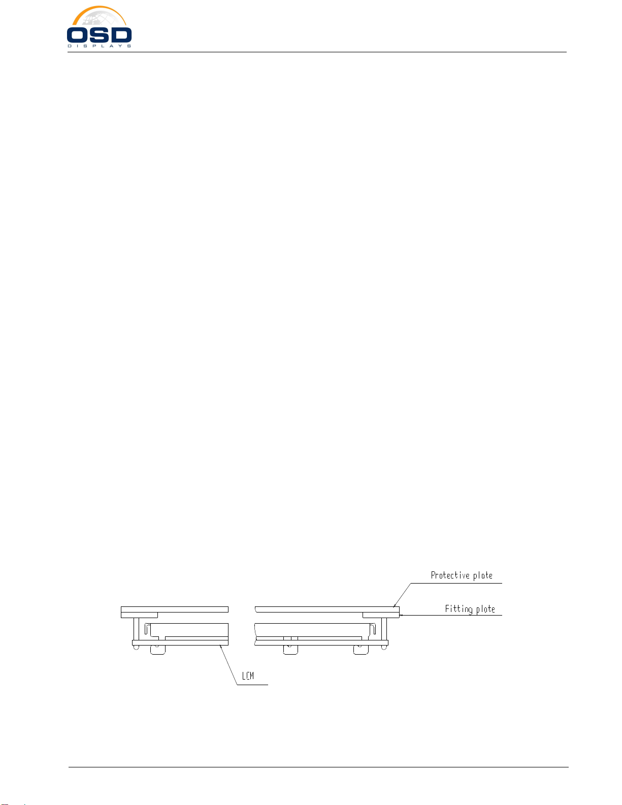
4.1 InstallingLCDModules
TheholeintheprintedcircuitboardisusedtofixLCMasshowninthepicturebelow.
Attendtothefollowing itemswheninstalling theLCM.
4.1.1 CoverthesurfacewithatransparentprotectiveplatetoprotectthepolarizerandLCcell.
4.1.2 Whenassembling theLCMintootherequipment,thespacertothebitbetweentheLCM
andthefittingplateshouldhaveenough heighttoavoidcausingstresstothemodule
surface,refertotheindividualspecificationsformeasurements.Themeasurement
toleranceshouldbe ±0.1mm.
Table of contents


