ozQRP DDS VFO 2 Instructions for use

DDS VFO 2 Construction Manual –Issue 1 Page 1
DDS VFO 2
CONSTRUCTION MANUAL

DDS VFO 2 Construction Manual –Issue 1 Page 2
Important
Please read before starting assembly
STATIC PRECAUTION
The DDS VFO kit contains the following components which can be
damaged by static discharge:
The DDS chip which is pre-soldered to the PCB and shipped in
an anti-static bag.
The microcontroller which is pre-programmed and shipped in
an anti-static bag.
Do not remove the devices from their protective anti-static bags until
you have taken precautions against static discharge.
If possible use an anti-static wrist strap and conductive mat.
These can be purchased readily from electronic retailers.
If these are not available then at least ensure you have
discharged yourself by touching an earthed metal surface.
Try not to directly touch the pins of the devices.
Ensure your soldering iron has an earthed tip.

DDS VFO 2 Construction Manual –Issue 1 Page 3
Contents
1Introduction..............................................................................................................................................................5
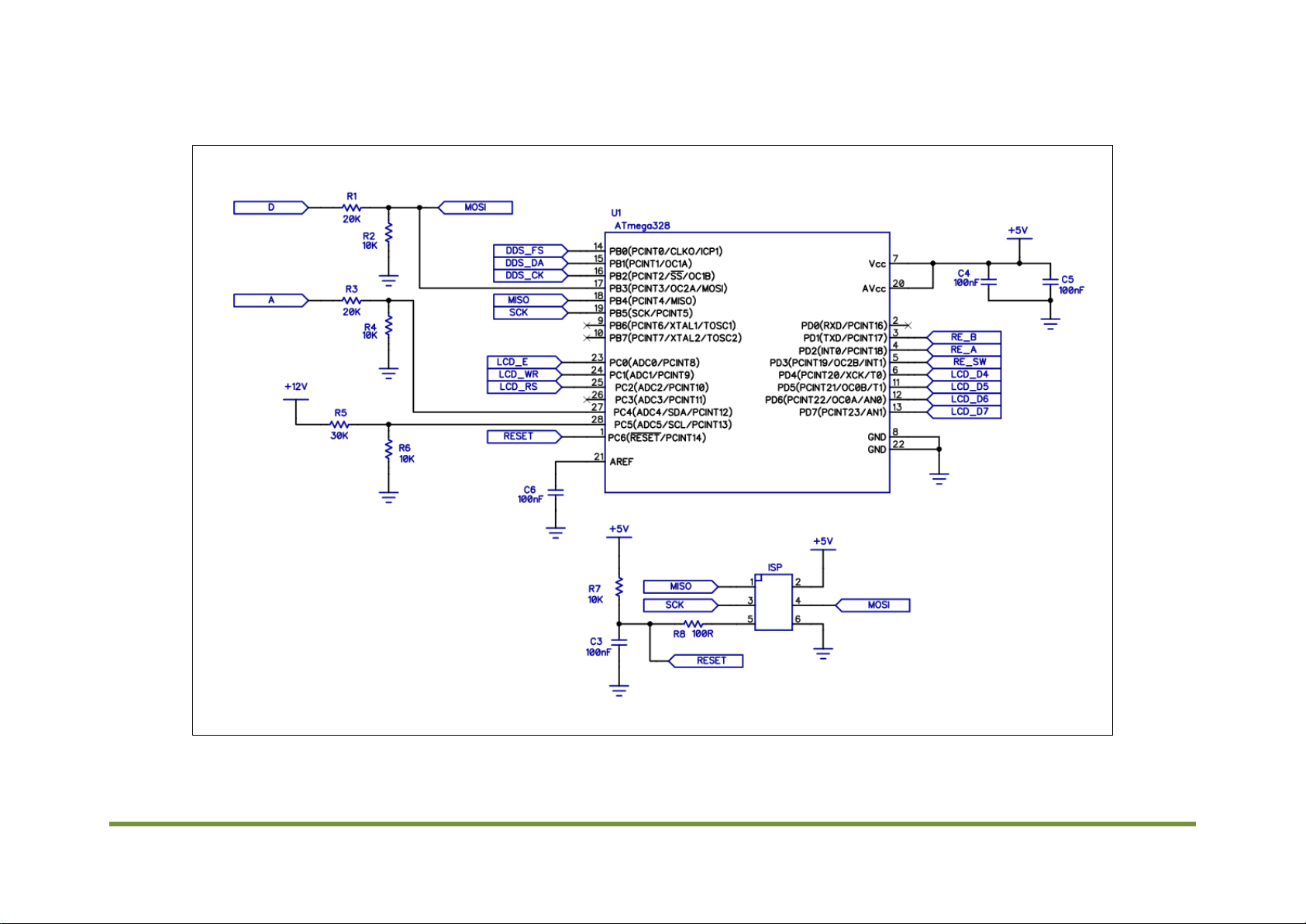
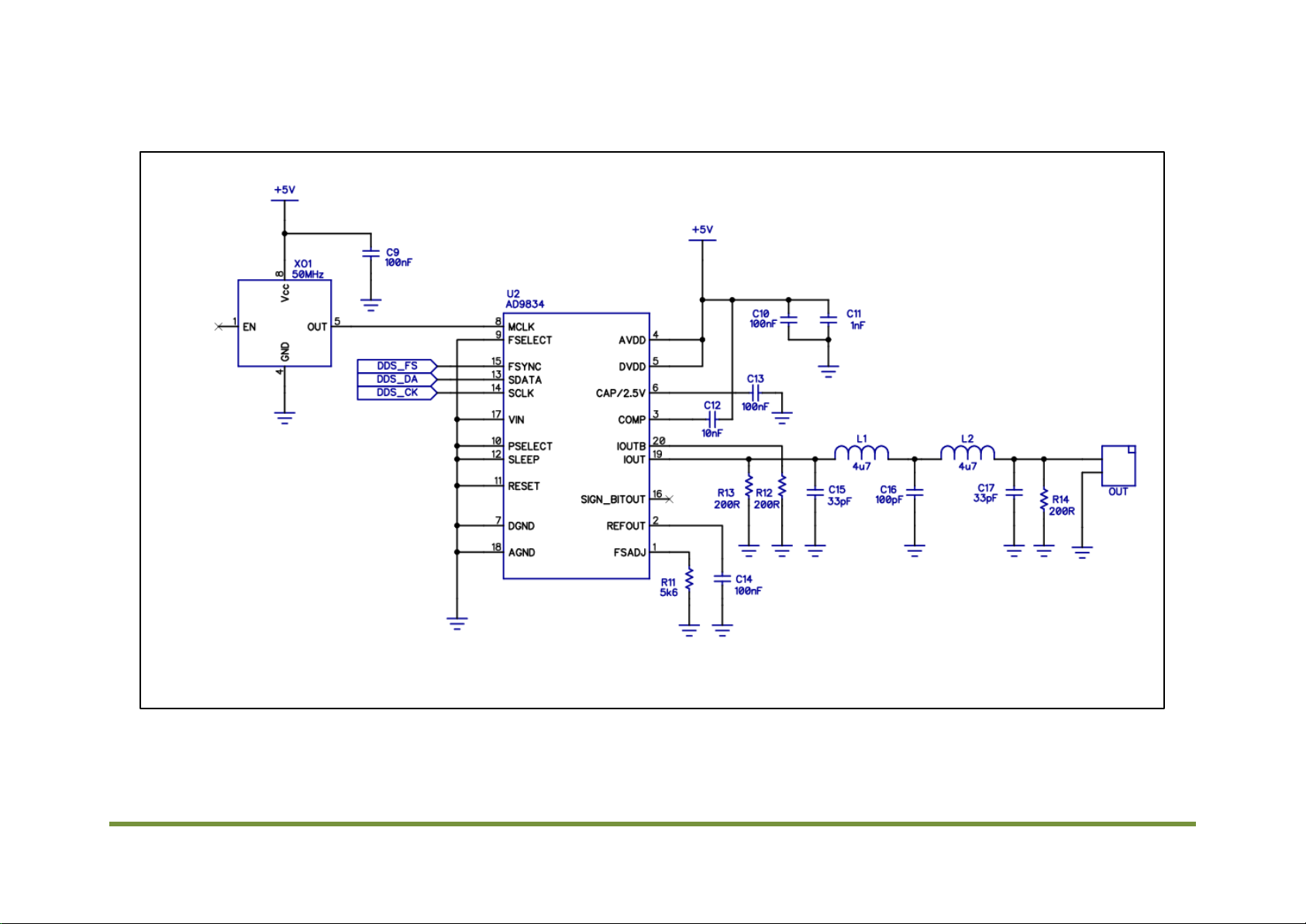
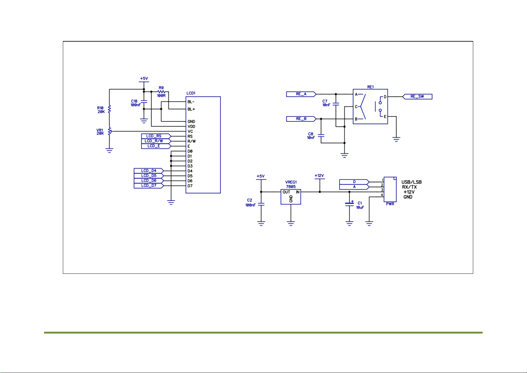
2Circuit Description .................................................................................................................................................6
3Kit Supplied Parts List........................................................................................................................................ 10
4The DDS VFO and the Superhet...................................................................................................................... 11
5Construction........................................................................................................................................................... 12
5.1 General............................................................................................................................................................ 12
5.2 Construction Steps..................................................................................................................................... 12
6First time power on............................................................................................................................................. 15
7Configuration......................................................................................................................................................... 16
7.1 Understanding options ............................................................................................................................ 16
7.2 Using the rotary encoder ........................................................................................................................ 18
7.3 Configuration Preview............................................................................................................................. 18
7.4 Entering New Values................................................................................................................................. 18
8Installing in a MST............................................................................................................................................... 20
8.1 Front Panel.................................................................................................................................................... 20
8.2 Wiring ............................................................................................................................................................. 21
8.3 Power .............................................................................................................................................................. 21
8.4 Output............................................................................................................................................................. 21
9Operation................................................................................................................................................................. 22
9.1 Power on........................................................................................................................................................ 22
9.2 Tuning............................................................................................................................................................. 22
9.3 Frequency steps.......................................................................................................................................... 22
9.4 RIT.................................................................................................................................................................... 22
9.5 Voltage Display............................................................................................................................................ 22
9.6 Frequency calibration .............................................................................................................................. 23
9.7 Voltage display calibration..................................................................................................................... 23
10 Notes ......................................................................................................................................................................... 24
10.1 Overclocking................................................................................................................................................. 24
10.2 DDS output.................................................................................................................................................... 24
10.3 Frequency range......................................................................................................................................... 24
10.4 LCD................................................................................................................................................................... 24
10.5 Firmware upgrades................................................................................................................................... 24

DDS VFO 2 Construction Manual –Issue 1 Page 4
List of Figures
Figure 1 CPU....................................................................................................................................................................... 7
Figure 2 DDS generator..................................................................................................................................................8
Figure 3 LCD, Rotary Encoder and Power Supply...............................................................................................9
Figure 4 Component overlay .................................................................................................................................... 14
Figure 5 Installing in a MST....................................................................................................................................... 20
Figure 6 MST3 cable..................................................................................................................................................... 21
Figure 7 LCD operating display ............................................................................................................................... 22

DDS VFO 2 Construction Manual –Issue 1 Page 5
1INTRODUCTION
The DDS VFO 2 is designed as a companion for the MST3 transceiver board although it could be
used with many other Superhet or Direct Conversion radios. It is simple to use having only one
control yet offers many advanced features. A kit of parts, with the DDS chip already loaded onto
PCB and blue backlit LCD, is available from www.ozQRP.com.
DDS VFO Features:
1. Stable frequency –no more drift!
2. Simple to operate using a single rotary encoder control with press button switch.
3. Bright 16 character by 2 line LCD display. Can also be used with a non-backlight display
to reduce current consumption if needed.
4. Output frequency range of 10KHz to 10MHz. Frequency range can be extended by
‘overclocking’ (see text).
5. Selectable 10KHz, 1KHz, 100Hz or 10Hz frequency steps.
6. RIT control allows fine adjustment of receive frequency without affecting the transmit
frequency.
7. Display of power supply voltage.
8. Display state of USB/LSB and TX/RX inputs.
9. Programmable IF frequencies. Separate high and low side IF frequencies ensure the
displayed frequency is the same as the transmitted frequency when changing sidebands.
10. Programmable option to save the current frequency and step value into memory. These
are re-loaded at power up.
11. Fine adjustment of frequency in configuration to allow for master clock tolerance.
12. Voltage display can be trimmed in configuration to allow for voltage reference errors.
13. Can be configured without an IF Offset to allow use as a signal generator or with Direct
Conversion transceivers.
14. Draws only around 50mA at 13.8V DC (with LCD backlight).
15. Spurious outputs at least -45dB.
16. Typically 300mV pk-pk sine wave output (200 ohms).
17. High quality double sided PCB with ground plane, plated through holes, solder mask and
silk screen.
18. Simple and easy to build using through hole components apart from one SMD chip. To
assist constructors the PCB comes shipped with the SMD chip already installed.

DDS VFO 2 Construction Manual –Issue 1 Page 6
2CIRCUIT DESCRIPTION
Integrated circuit U2 is an Analog Devices AD9834 Direct Digital Synthesis (DDS) chip and
forms the heart of the DDS VFO. A 50MHz crystal oscillator module supplies the master clock
and gives usable output frequencies up to a quarter of that value or 12.5MHz.
The DDS is controlled by a 3 wire serial data bus from microcontroller U1.The microcontroller is
an Atmel ATmega328 and runs an internal 8MHz clock which avoids the use and expense of an
external crystal.
A rotary encoder produces quadrature signals when rotated and one line is fed into the
microcontroller interrupt input and becomes the reference input. Once an interrupt is detected
the state of the other input is read and the direction determined. The rotary encoder also
incorporates a press button switch and is used for a number of functions as described later. U1
incorporates pull-up resistors for the encoder inputs so they are normally held high and
capacitors C7 and C8 help filter out switch bounce.
The microcontroller has an internal analog to digital converter (ADC) which uses the 5 volt rail
as a reference. The ADC measures the incoming power supply rail via a resistive attenuator
formed with R5 and R6. The calculated value is displayed on the LCD during use.
The A input is used to monitor the TX/RX state, while the D input is used to detect the state of
the USB/LSB switch. The inputs expect a nominal +12 Volt to 0V state change and are buffered
by resistive attenuators to protect the microprocessor inputs.
The PCB also includes an ISP connector to allow future software upgrades without having to
remove the chip from its socket.
Most of the remaining pins of U1 are dedicated to driving the LCD in 4 bit mode. R9 sets the
backlight current and may be left out if a non-backlight LCD is used. VR1 adjusts the LCD
contrast and normally only needs to be set once at the commissioning stage.
The outputs from the DDS chip are current sources and the output is converted to a voltage by
the 200 ohm resistors R12 and R13. The full scale value of the current and hence the pk-pk
output voltage is set by the 5.6K ohm resistor R11. The output is passed through a simple 5 pole
low pass filter to attenuate unwanted high frequency components.
R14 is used to terminate the filter if the external load is high impedance. In most circumstances
it can be left off the board.
The incoming power supply is regulated to 5V by a 7805 1A regulator which mounts flat on the
PCB to act as a heatsink.

DDS VFO 2 Construction Manual –Issue 1 Page 7
Figure 1 CPU

DDS VFO 2 Construction Manual –Issue 1 Page 8
Figure 2 DDS generator

DDS VFO 2 Construction Manual –Issue 1 Page 9
Figure 3 LCD, Rotary Encoder and Power Supply

DDS VFO 2 Construction Manual –Issue 1 Page 10
3KIT SUPPLIED PARTS LIST
Quantity
Comment
Designator
Capacitors
2
33pF 50V disc ceramic
C15, C17
1
100pF 50V disc ceramic
C16
1
1nF 50V disc ceramic
C11
3
10nF 50V ceramic MLCC
C7, C8, C12
10
100nF 50V ceramic MLCC
C2, C3, C4, C5, C6, C9, C10, C13, C14, C18
1
10uF 25V RB electrolytic
C1
Resistors
2
100R 1/4W 1% resistor
R8, R9
3
200R 1/4W 1% resistor
R12, R13, R14
1
5.6K 1/4W 1% resistor
R11
4
10K 1/4W 1% resistor
R2, R4, R6, R7
3
20K 1/4W 1% resistor
R1, R3, R10
1
30K 1/4W 1% resistor
R5
1
20K horizontal trimpot
VR1
Semiconductors
1
ATmega328 - 28pin DIP
U1
1
AD9834 DDS 20 pin TSSOP
U2
1
7805 5V regulator TO220
VREG1
1
50MHz crystal oscillator module
XO1
1
16 x 2 LCD with backlight.
LCD1
Inductors
2
4.7uH moulded RF choke
L1, L2
Hardware
1
DDS VFO PCB
1
28 pin DIP narrow IC socket
1
3 pin x 2 row 2.54mm pitch header
HDR1 (ISP)
1
Rotary Encoder
RE1
1
4 pin 2.54mm pitch header RA
SK1 (PWR)
1
2 pin 2.54mm pitch header RA
SK2 (OUT)
1
4 pin plug + pins
1
2 pin plug + pins
4
12mm long 3mm nylon spacer
4
2.5mm x 20mm screws
4
2.5mm nuts
1
16 way SIL male pin header
1
16 way SIL female pin header
1
3mm x 10mm screw
1
3mm nut

DDS VFO 2 Construction Manual –Issue 1 Page 11
4THE DDS VFO AND THE SUPERHET
When the DDS VFO is used in a Superhet transceiver, the relationship between the displayed
frequency, the DDS output frequency and the actual transmit frequency can be confusing. This
section contains an example to help illustrate the relationship. The example assumes a DDS VFO
connected to a MST operating LSB on the 40M band.
The balanced modulator in the MST takes the nominal 10MHz carrier (BFO) signal and mixes
this with the audio signal when you speak. The output of the balanced modulator is comprised
of an upper sideband (USB) and a lower sideband (LSB) signal centered on the carrier
frequency. The carrier is not present at the output (suppressed) and so we use the term Double
Sideband Suppressed Carrier modulation or simply DSB. The DSB signal is applied to the crystal
filter.
The filter’s upper skirt is at 10MHz, and so the LSB is passed by the crystal filter, while the USB
is blocked. The LSB signal is then mixed with the output of the DDS VFO to obtain the final
transmit signal.
We will assume the DDS VFO is configured for an IF frequency of 10MHz, and display frequency
of 7.100MHz.
The DDS computes the output frequency to be 10.000MHz - 7.100MHz = 2.900MHz.
The final transmitted signal will be 10.000MHz - 2.900MHz = 7.100MHz.
Now let's assume that we want to move the carrier frequency 300Hz higher. This could be due
to a slightly higher crystal filter response or after testing we find the USB is not suppressed
sufficiently.
The new carrier frequency will be 10.0003MHz, however the DDS VFO will still be programmed
for an IF frequency of 10.000MHz and generate an output frequency of 2.9MHz. As a result the
displayed frequency will be 10.000MHz - 2.900MHz = 7.100MHz, but the actual transmit
frequency will be: 10.0003MHz - 2.900MHz = 7.1003MHz.
This creates an error situation where the LCD displayed frequency and the actual
transmit frequency are not the same.
To fix this we need to measure the actual suppressed carrier frequency and re-configure the
DDS VFO IF frequency parameter.
Using this example we would now configure the DDS VFO with IF frequency of 10.0003MHz.
The DDS output frequency will now become 10.0003MHz - 7.100MHz = 2.9003MHz, and the
final transmitted signal will be 10.0003MHz - 2.9003MHz = 7.100MHz.
The displayed frequency now correctly matches the transmitted signal frequency.

DDS VFO 2 Construction Manual –Issue 1 Page 12
5CONSTRUCTION
5.1 GENERAL
The DDS VFO is a built on a high quality fiberglass PCB. The PCB is doubled sided with tracks on
both sides along with a ground plane. The holes are plated through and so it is not necessary to
solder both sides to make connections. To assist construction the component overlay is screen
printed on both sides and a solder mask is included to guard against solder bridges.
The ground plane is substantial and can sink quite a bit of heat from low wattage soldering irons
so ensure you use a good quality iron that can sustain the power required. You may find that
sometimes solder doesn’t appear to flow through to the top side. This is not necessarily a
problem because the plated through holes make a connection to the top side automatically.
Another point to consider is that plated through holes consume more solder than non-plated
holes and makes it more difficult to remove components.
The lesson is to double check the values and orientation of components before
installation.
There isn’t a ‘best’ scheme for loading the components, however, the suggested procedure is to
load the smaller components first and then work upwards.
5.2 CONSTRUCTION STEPS
Refer to the parts list and Figure 4 when installing the components.
Step 1: Resistors
If in doubt check the values with a multimeter before soldering. Pass the pigtails through
from the top and bend out slightly underneath to hold them in place. Turn the PCB over and
press down slightly to make them rest against the surface and then solder. Cut off the excess
pigtail with side cutters. The trimpot can also be installed at this stage. If the DDS VFO is used
with the MST3, R14 is not installed. It is included on the PCB to terminate the filter if required
when used with high impedance loads.
Step 2: RF chokes
These are not polarized and can go in either way. Make sure they sit flat against the board
before soldering.
Step 3: Capacitors
Install the capacitors with minimal lead length. The electrolytic is the only polarized capacitor
and the positive lead points towards the edge of the PCB.

DDS VFO 2 Construction Manual –Issue 1 Page 13
Step 4: IC socket
The IC socket is installed next with the notch facing the right side of the PCB.
Step 5: Crystal oscillator module
Ensure pin 1 of the oscillator module faces the bottom left of the PCB.
Step 6: 5 volt regulator
The regulator lays flat against the PCB so needs the leads bent at right angle to fit through the
holes in the PCB. Insert into the PCB holes and secure with a 3mm screw and nut before
soldering the leads.
Step 7: Connectors
The Output connector is a 2 pin right angle header while the Power connector is a 4 pin right
angle header. Push them into the PCB so they lay flat against the board and then solder.
The ISP header is an un-shrouded 3 pin x 2 row header and the shorter pins are inserted into
the PCB and soldered.
The LCD connector is a 16 way male pin header and is mounted on the reverse side with the
short ends of the pins located in the PCB. Ensure it is pushed in completely and solder the end
pins first and check it is at right angle to the PCB before soldering the remaining pins.
Step 8: Rotary encoder
The rotary encoder is mounted on the reverse side. Insert into the holes and check that it is at
right angle to the board before soldering. It is not necessary to completely fill the mechanical
mounting holes in the PCB with solder.
Step 9: Microcontroller
Remove the microcontroller from the bag and insert into the IC socket ensuring pin 1 points to
the top right of the PCB towards the contrast control. It may be necessary to squeeze the rows of
pins slightly together to get it to fit into the socket.
Step 10: LCD
Solder a 16 way female pin header to the rear side of the LCD PCB.
The LCD can then be mounted onto the DDS VFO and mate with the 16 way male pin header.
Place four 12mm long nylon spacers between the LCD and DDS VFO PCB at each corner and
secure the assembly with 2.5mm screws and nuts.

DDS VFO 2 Construction Manual –Issue 1 Page 14
Figure 4 Component overlay

DDS VFO 2 Construction Manual –Issue 1 Page 15
6FIRST TIME POWER ON
Before applying power check the board over one more time. Look for solder bridges and
components in the wrong way. A moment spent here may save a lot of frustrating time later on.
Once you are satisfied connect the DDS VFO to a power supply between 9 and 15V DC. If the
power supply has current limiting set this to about 100mA.
Apply power and check that the LCD backlight turns on. Also check with a multimeter that the
output of the regulator is between 4.75 and 5.25V DC. The power supply current should be
around 50mA. If the LCD installed is not the one supplied in the kit the current may be different
depending on the backlight characteristics.
If the readings are way outside this range turn off immediately and look for problems.
At this stage you may or may not see anything on the LCD. Most likely this is because the LCD
contrast has not been set. Adjust the contrast trimpot until the characters are clear and easy to
read.
Turn the power off then on again and check that the first thing displayed is the firmware version
number. This is then followed by the operating display.
As the DDS VFO has not been configured the LCD will display default settings. These are
frequency of 7.1MHz and a 1KHz Step. Verify with an oscilloscope or a frequency counter that
the DDS is outputting a 2.9MHz sine wave signal of around 300mV pk-pk.

DDS VFO 2 Construction Manual –Issue 1 Page 16
7CONFIGURATION
7.1 UNDERSTANDING OPTIONS
Master Clock
The DDS VFO requires a master clock to generate the output frequencies. The firmware can
accept three clock frequencies of 50MHz, 80MHz or 100MHz. The 50MHz clock rate is the
default setting while the other options allows ‘over clocking’ of the DDS chip to generate higher
frequencies if required. See section 10 for more details.
IF Offset
When the IF Offset is set to Yes, the LCD will display the desired transmit frequency while the
actual DDS signal frequency will be equal to the difference between the IF and transmit
frequencies.
For example, the MST3 transceiver employs a 10MHz IF frequency. If the desired transmit
frequency is 7.1MHz then the DDS VFO frequency would be 10 –7.1 = 2.9MHz.
The relationship between the IF frequency, DDS VFO frequency and transmit frequency when
used with the MST3 is shown below:
Band
IF frequency
DDS VFO frequency
Transmit frequency
80M
10MHz
6.5MHz
3.5MHz
40M
10MHz
3MHz
7MHz
20M
10MHz
4MHz
14MHz
17M
10MHz
8MHz
18MHz
Note that the DDS VFO firmware assumes that the DDS VFO frequency is always
below the IF frequency.
If the IF Offset is set to No the DDS output frequency will be the same as the displayed
frequency. This is the setting selected when the DDS VFO is to be used as a general purpose
signal generator or with a Direct Conversion receiver.
IF Freq High and IF Freq Low
To generate an accurate output frequency the DDS VFO must know the exact IF frequency. To do
this the frequency must be measured using a frequency counter and the value entered at
configuration. If not the default values will be used and the displayed frequency may not
accurately match the transmit frequency.
Also, the MST3 moves the IF frequency when changing sidebands by about 3KHz. So that the
displayed frequency and the actual transmitted frequency are matched it is necessary to enter
both upper and lower IF frequencies. Using these values the DDS VFO firmware automatically
adjusts the output frequency when sidebands are changed.

DDS VFO 2 Construction Manual –Issue 1 Page 17
Band
This option is used in conjunction with the IF Freq to determine the actual DDS frequency.
30S Freq Save
This option enables automatic saving of the current frequency and step in EEPROM so that it is
recalled the next time the DDS VFO is powered on. The EEPROM has a maximum specification of
100,000 write/erase cycles, so to protect it from excessive writes, the save is performed only
once per frequency change and only after a 30 second idle period has elapsed. If the encoder is
operated so that there is less than 30 seconds between changes no saves will be performed.
Freq Calibrate
The DDS frequency is directly related to the master clock frequency. Due to component
tolerances the master clock may not be exact and as a consequence the transmitted signal will
be slightly off frequency when compared to the display frequency. This option allows trimming
of the DDS output frequency in firmware. The range is plus and minus 500Hz in 10Hz steps.
Volts Calibrate
The microcontroller measures the battery voltage using an analog to digital converter with the
+5V rail as the reference voltage. As the +5V rail is supplied by an ordinary 7805 regulator, it
may not be exactly +5V, and therefore the displayed voltage may not be correct. This option
allows the displayed value to be trimmed by plus and minus 1V in 0.1V steps to match the
correct value.
Frequency
When the IF Offset option is set to No the DDS VFO displayed frequency is the same as the
transmit frequency. This option allows the initial frequency to be set.

DDS VFO 2 Construction Manual –Issue 1 Page 18
7.2 USING THE ROTARY ENCODER
In Configuration the rotary encoder has four states:
1. Rotate clockwise. Used to increment values
2. Rotate counter-clockwise. Used to decrement values.
3. Short (less than 1 second) press of the encoder button. Used to toggle between options
or move the cursor to the right.
4. Long (greater than 1 second) press of the encoder button. Used to move to next
configuration menu.
When a configuration menu is exited the selected values are automatically stored in
memory.
7.3 CONFIGURATION PREVIEW
The configuration parameters are stored in non-volatile memory and recalled at power up.
During configuration the current parameters are displayed as each menu is accessed. By simply
stepping through the menus without making changes the current parameters can be viewed.
7.4 ENTERING NEW VALUES
1. Hold down the encoder button and apply power to the DDS VFO.
2. Wait until the LCD displays Configuration (about 3 seconds) and then release the
button.
3. The Master Clock menu will be displayed. Pressing the encoder button for less than 1
second will toggle through the clock options. Once completed press the encoder button
for longer than 1 second and release.
4. The IF Offset menu will be displayed. Pressing the encoder button for less than 1
second will toggle between Yes and No. Once completed press the encoder button for
longer than 1 second and release. If this option is set to No, the IF Freq High and IF Freq
Low menus will be bypassed.
5. The IF Freq High menu will be displayed and the cursor will be positioned on the
10MHz digit. Rotating the encoder clockwise increments the digit while rotating the
encoder anti-clockwise decrements the digit. Pressing the encoder button for less than 1
second will step the cursor onto the next digit. Once completed press the encoder
button for longer than 1 second and release.
6. The IF Freq Low menu will be displayed and the cursor will be positioned on the
10MHz digit. Rotating the encoder clockwise increments the digit while rotating the
encoder anti-clockwise decrements the digit. Pressing the encoder button for less than 1
second will step the cursor onto the next digit. Once completed press the encoder
button for longer than 1 second and release. If the IF Offset option has been set to Yes
the Frequency menu will be bypassed.
7. The Frequency menu will be displayed and the cursor will be positioned on the 10MHz
digit. Rotating the encoder clockwise increments the digit while rotating the encoder
anti-clockwise decrements the digit. Pressing the encoder button for less than 1 second
will step the cursor onto the next digit. Once completed press the encoder button for
longer than 1 second and release.

DDS VFO 2 Construction Manual –Issue 1 Page 19
8. The Band menu will be displayed. Pressing the encoder button for less than 1 second
will toggle through the band options. Once completed press the encoder button for
longer than 1 second and release.
9. The 30 second Freq Save menu will be displayed. Pressing the encoder button for less
than 1 second will toggle between the Yes and No options. Once completed press the
encoder button for longer than 1 second and release.
10. The Freq Calibrate menu will be displayed. Rotating the encoder clockwise increments
the value while rotating the encoder anti-clockwise decrements the value. Pressing the
encoder button for less than 1 second will toggle the plus/minus sign. Once completed
press the encoder button for longer than 1 second and release.
11. The Volts Calibrate menu will be displayed. Rotating the encoder clockwise increments
the value while rotating the encoder anti-clockwise decrements the value. Pressing the
encoder button for less than 1 second will toggle the plus/minus sign. Once completed
press the encoder button for longer than 1 second and release.
12. The DDS VFO will then store the values in non-volatile memory and return to normal
operation.

DDS VFO 2 Construction Manual –Issue 1 Page 20
8INSTALLING IN A MST
8.1 FRONT PANEL
The DDS VFO is simply screwed to the inside of the front panel of the MST. The DDS VFO PCB is
set back from the panel using threaded spacers to allow room for the LCD. If you use the LCD
supplied in the kit the distance will be 22mm. This can be made up of a 10mm spacer and 12mm
spacer or a single 22mm spacer or a long screw and nuts.
A countersink screw is used on the front panel to provide a flush surface for the front panel
label to sit. If preferred round head screws can be used which means that holes need to be made
in the label and also the heads will be visible from the front.
If a LCD is used that does not incorporate a backlight it will not be as high and so the length of
the screws and spacers need to be reduced accordingly.
The general mounting arrangement is shown in Figure 5.
.
Figure 5 Installing in a MST
12mm x 3mm tapped
nylon spacer
10mm x 3mm tapped
nylon spacer
3mm x 16mm C/S screw
Front panel
PCB
LCD
3mm x 6mm screw
Table of contents