Paia 9710 Guide

9710 VCA 1
000216
Model 9710
Assembly and Using Manual
Triple VCA w/Modulator
(c) 2000 PAiA Electronics, Inc.
Ordinarily, Voltage Controlled Amplifiers are pretty
routine. But by combining 2 VCAs, a Balanced
Modulator, a White Noise Source and Envelope
Generator in a single module and interconnecting
them with a powerful normalization design, the 9710
redefines what a VCA module should be.
At the highest level, you can use the 9710 like a
traditional VCA but with the added convenience of a
built-in Voltage Controlled Input Submixer and ADSR
Envelope Generator. This configuration of elements
allows a couple of signals to be mixed together
before being processed by the VCA which is con-
trolled by the ADSR. It would ordinarily require three
or four modules and a handful of patch cords but is
embodied as a single element in the 9710.
And the versatility of individual modules is not
sacrificed because patch cords can be used to
override the normalization and access progressively
lower level functional sub-groups or even the indi-
vidual elements.

2 9710 VCA 000216
ASSEMBLING THE 9710 Triple VCA W/Modulator
Before beginning assembly, go through the manual.
Look at the drawings. Feel the parts. You’re
naturally eager to plunge right in, but take a few
deep breaths first. Check the parts supplied against
the packing list on the last page of this manual.
In some cases, notes packed with the parts will
be used to call your attention to special situations.
These notes may be in the yellow "MISSING PARTS"
postcard. If parts are missing please notify PAiA at
Notice that each step in the manual is marked with
a checkoff box like this:
DESIGNATION VALUE COLOR CODE
( ) R27 100 ohm brown-black-brown
Checking off each step as you do it may seem
silly and ritualistic, but it greatly decreases the
chance of omitting a step and also provides
some gratification and reward as each step is
completed.
Numbered figures are printed in the Illustrations
Supplement in the center of this manual. These pages
may be removed for easy reference during assembly.
THE CIRCUIT BOARD
The 9710 VCA is built on a double-sided circuit
board. No special preparation or cleaning is necessary
before assembly. The "top" of the board is the side that
is printed with component designations and parts are
mounted from this side. The "bottom" of the board is
also called the solder side and is masked with a
conformal coating to lessen the chance of solder bridges.
Solder pads are tin-lead plated for ease of soldering and
assembly.
TOOLS
You’ll need a minimum of tools to assemble the kit
- a small pair of diagonal wire cutters and pliers,
screwdriver, sharp knife, ruler, soldering iron and

9710 VCA 3
000216
solder.
Modern electronic components are small (in case you
hadn’t noticed) and values marked on the part are
often difficult to see. Another handy tool for
your bench will be a good magnifying glass. Also
use the magnifier to examine each solder joint as
it is made to make sure that it doesn’t have any of
the problems described in the SOLDERING section
which follows.
SOLDERING
Select a soldering iron with a small tip and a
power rating not more than 35 watts. Soldering
guns are completely unacceptable for assembling
solid state equipment because the large magnetic
field they generate can damage components.
Use only a high quality 60/40 alloy rosin core solder
(acid core solder is for plumbing, and silver solder is
for jewelry - neither is for electronics work). A proper solder
joint has just enough solder to cover the soldering
pad and about 1/16-inch of lead passing through it.
There are two improper connections to beware of:
Using too little solder will sometimes result in a
connection which appears to be soldered when
actually there is a layer of flux insulating the
component lead from the solder bead. This
situation can be cured by reheating the joint and
applying more solder.
Too much solder may produce a conducting bridge of
excess solder between adjacent pads causing a
short circuit. If WAY too much solder is used it may flow
through the hole and cause bridges between conductors
on the component side of the board or even impede the
action of mechanical components such as trimmer
potentiometers. Accidental bridges can be cleaned off by
holding the board upside down and flowing the excess
solder off onto a clean, hot soldering iron.
Use care when mounting all components. Never force
a component into place.
Special thanks to the
beta crew -
Scott Lee
Tim Furry
Johnny Klonaris
David Hillel Wilson
and me - John Simonton

4 9710 VCA 000216
Resistors
Solder each resistor in place following the parts placement
designators printed on the circuit board and the
assembly drawing fig 1. Note that resistors are nonpolarized
and may be mounted with either lead in either of the holes
in the board. Before mounting each resistor, bend its leads
so that they are at a right angle to the body of the part. Put
the leads through the holes and then push the resistor firmly
into place. Cinch the resistor in place by bending the leads
on the solder side of the board out to an angle of about
45 degrees. Solder both ends of each resistor in place
as you install it. Clip each lead flush with the solder joint
and save a few of the clippings for use in later steps.
A tip: If you can't find the location for a resistor, go on to the
next one and come back. DO NOT CHECK OFF A PART
UNTIL IT IS INSTALLED AND SOLDERED.
DESIGNATION VALUE COLOR CODE A-B-C
listed below:
100 brown-black-brown
( ) R28 ( ) R33 ( ) R40 ( ) R44
listed below:
100k brown-black-yellow
( ) R4 ( ) R5 ( ) R8 ( ) R9
( ) R11 ( ) R14 ( ) R65 ( ) R67
( ) R73 ( ) R89 ( ) R92 ( ) R94
( ) R96 ( ) R105
listed below:
10k brown-black-orange
( )R12 ( ) R13 ( ) R21 ( ) R50
( ) R64 ( ) R66 ( ) R91 ( ) R93
( ) R95 ( ) R100 ( ) R102 ( ) R104
( ) R108 ( ) R118
( ) R38 10m brown-black-blue
( ) R48 10m brown-black-blue
listed below:
120k brown-red-yellow
( ) R3 ( ) R6 ( ) R7 ( ) R10
( ) R19 ( ) R76
( ) R15 1500 brown-green-red
( ) R18 1500 brown-green-red
( ) R41 15k brown-green-orange
( ) R42 15k brown-green-orange

9710 VCA 5
000216
listed below:
18k brown-grey-orange
( ) R71 ( ) R81 ( ) R85 ( ) R87
listed below:
1k brown-black-red
( ) R25 ( ) R26 ( ) R80 ( ) R99
( ) R107
listed below:
220 red-red-brown
( ) R35 ( ) R36 ( ) R45 ( ) R46
( ) R98
( ) R20 2200 red-red-red
listed below:
220k red-red-yellow
( ) R16 ( ) R17 ( ) R75 ( ) R78
( ) R88 ( ) R97
listed below:
22k red-red-orange
( ) R23 ( ) R37 ( ) R47 ( ) R60
( ) R69
listed below:
33 orange-orange-black
( ) R1 ( ) R2 ( ) R62 ( ) R68
( ) R82 3300 orange-orange-red
listed below:
330k orange-orange-yellow
( ) R53 ( ) R55 ( ) R58 ( ) R83
( ) R84
listed below:
33k orange-orange-orange
( ) R51 ( ) R52 ( ) R70 ( ) R103
( ) R29 390 orange-white-brown
( ) R30 3900 orange-white-red
( ) R32 3900 orange-white-red
( ) R79 3900 orange-white-red
( ) R74 4.7meg yellow-violet-green
( ) R27 470k yellow-violet-yellow
( ) R86 470k yellow-violet-yellow
listed below:
47k yellow-violet-orange
( ) R31 ( ) R49 ( ) R54 ( ) R56
( ) R57 ( ) R59 ( ) R90 ( ) R101
( ) R106 ( ) R119 ( ) R120

6 9710 VCA 000216
( ) R22 6800 blue-grey-red
( ) R39 910k white-brown-yellow
( ) R43 910k white-brown-yellow
listed below:
91k white-brown-orange
( ) R61 ( ) R63 ( ) R72 ( ) R77
Disk Capacitors
Many of the capacitors used in the 9730 are nonpolarized
Ceramic Disk types. For each of these, either lead can go in
either of the holes in the circuit board. The leads are already
parallel to each other but still may need to be bent slightly to
match the spacing of the circuit board holes. Like the resistors,
insert the leads of these parts through the holes in the board
and push the part against the circuit board as far as it wants to go.
Don't force it, it's OK if it sits a little off the board.
Capacitors are often marked with obscure codes that
indicate their values. The 3 digit number that specifies
value may be preceded or followed by letters indicating
such things as tolerance. If you get confused about
which capacitors are which, it may help to group them
by same type and check them against quantities on the
packing list at the end of this manual.
DESIGNATION VALUE MARKING
( ) C18 0.005 502
( ) C22 0.005 502
( ) C23 0.005 502
listed below:
0.01 103
( ) C3 ( ) C5 ( ) C7 ( ) C9
( ) C10 ( ) C13 ( ) C17
listed below:
100pF 100
( ) C8 ( ) C11 ( ) C12 ( ) C14
( ) C15
Ceramic Disk
Capacitors

9710 VCA 7
000216
Electrolytic Capacitors
The remaining capacitors are electrolytic types.
Unlike the previous components, electrolytic
capacitors are polarized and the leads are not
interchangeable. Leads are marked "+" and/or "-"
and the "+" lead must go through the "+" hole in the
circuit board. Frequently the positive lead of the
capacitor is significantly longer than the negative lead.
Usually the Negative lead of the capacitor is marked rather
than the positive. It naturally goes through the unmarked hole.
Capacitors supplied with specific kits may have a higher
Voltage (V) rating than the minimum specified below.
DESIGNATION VALUE
( ) C20 10uF / 15V
( ) C21 10uF / 15V
( ) C16 1uF / 15V
( ) C1 220uF / 25V
( ) C2 220uF / 25V
( ) C19 33uF / 15V
( ) C4 4.7uF / 15V
( ) C6 4.7uF / 15V
Diodes
Like the Electrolytic Capacitors, diodes are polarized
and must be installed so that the lead on the banded
end of the part corresponds to the banded end of the
designator on the circuit board. Bend the leads so they
are at right angles to the body of the part and insert
them through the holes provided in the circuit board.
Diodes are also somewhat heat sensitive so the
soldering operation should be done as quickly as possible.
DESIGNATION TYPE
listed below: 1N4148 Silicon Diode
( ) D1 ( ) D2 ( ) D3 ( ) D4
( ) D5 ( ) D6 ( ) D7
Note diode
polarity band

8 9710 VCA 000216
Transistors
Install the transistors by inserting their three leads
through the holes provided for them in the circuit board.
Note that the transistors are polarized by the flat side
of the case. When the transistors are properly
installed this flat will align with the corresponding mark
on the circuit board legending.
Notice that two different types of transistors (2N3904 and 2N3906)
are used. The type will be written on the body of the part.
Two of the transistors have been specially selected to have
matching characteristics and will be packed together.
Keeping this pair together is important for optimum circuit
performance. Since they are matched, it makes no difference
which transistor is used for which designation.
DESIGNATION TYPE
( ) Q3/Q4 2N3904 NPN Si Transistor Matched Pair
One transistor has been selected for use as a noise
source and has one of its leads cut short.
( ) Q5 2N3906 Selected for noise.
Install the remaining transistors as follows:
listed below: 2N3906 PNP Silicon Transistor
( ) Q1 ( ) Q2 ( ) Q6 ( ) Q7
( ) Q13
listed below: 2N3904 NPN Silicon Transistor
( ) Q8 ( ) Q9 ( ) Q10 ( ) Q11
( ) Q12 ( ) Q14 ( ) Q15
Trimmer Potentiometers
The two trimmer potentiometers surface mount to the
board rather than having their leads pass through it.
First "tin" the trimmer mounting pads on the circuit boar
by melting a little solder onto them. Solder the trimmer
to the board by holding the pins against the tinned pads
and remelting the solder.
The straight line of the pc
graphic symbol corresponds
to the flat face of the
transistor case.
Note flat
Q5 has one lead removed
Trimmer potentiometers surface
mount by tinning the mounting
pads and remelting the solder to
the component pins
Note cut-off
lead

9710 VCA 9
000216
DESIGNATION VALUE MARKING
( ) R26 100k 100K
( ) R34 100k 100K
Integrated Circuits
Of all the parts, the ICs are the most easily damaged
and should be treated with some respect. In particular,
they may be destroyed by discharges of static electricity.
Modern ICs are not nearly as sensitive to this kind
of damage as were earlier versions, but it is still good
practice to handle these parts as little as possible.
Also good practice: don't wear nylon during assembly.
Don't shuffle around on the carpet immediately before
assembly (or if you do, touch a lamp or something to
make sure you're discharged). Don't be intimidated.
It's rare for parts to be damaged this way.
ICs are polarized in one or both of two ways; A dot
formed into the case of the IC corresponding to pin 1
or a semicircular notch that indicates the end of the
package with pin 1. Take care that this polarizing
indicator corresponds to the similar indicator on the
circuit board graphics.
The pins of the ICs may be splayed somewhat and not
match the holes in the circuit board exactly. Carefully
re-form the leads if necessary so that they are at right
angles to the part.
Solder each IC in place as it is installed by initially
soldering two pins in diagonal corners of the
pattern. Make sure that the part is seated firmly
against the circuit board by pressing it down while re-
melting the solder joint at first one corner, then
the other. Finally, solder the remaining
connections.
DESIGNATION PART NO. DESCRIPTION
( ) IC3 LM324 Quad OpAmp
( ) IC4 LM1496 Balanced Modulator
( ) IC5 LM13600 Dual OTA
( ) IC6 LM324 Quad OpAmp
( ) IC7 LM324 Quad OpAmp
LM13600
16 pins
Note pin 1
LM324
LM1496
14 pins

10 9710 VCA 000216
Voltage Regulators
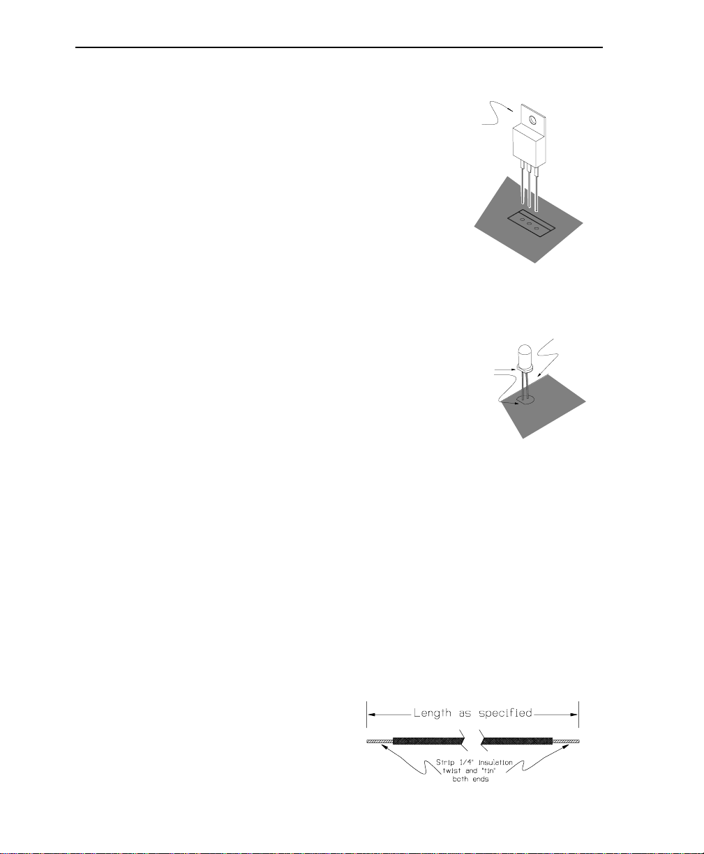
The voltage regulators are polarized and
must be mounted so that their tabs correspond to
the tab markings on the circuit board graphics.
Solder all three leads and clip any excess off
flush with the solder joint.
( ) IC1 7912 -12V Voltage Regulator
( ) IC2 7812 +12V Voltage Regulator
LEDs
LEDs are polarized by the flat in the collar at the base
of part. When properly installed, this flat will align with
the corresponding flat in the LED symbol printed on
the circuit board.
When the 9730 is installed behind its front panel, the
LED will engage the hole in the front panel and be
supported by its leads. Install the LED by pushing it's
two leads through the holes in the circuit board. With
3/8" of space between the bottom of the LED and the
circuit board, solder one lead. Check spacing and polarization
before soldering the second lead and trimming both leads
off flush with the solder joint.
DESIGNATION TYPE
( ) LED1 Red LED
"Flying" Wires
(i.e. those which go from circuit board to panel mounted parts.)
In the following steps, wires will be soldered to the 9730 board
which in later steps will be connected to the front panel controls
and switches. At each step, cut a piece of wire to the specified
length and strip 1/4" of insulation from each end. Twist the
exposed wire strands together and "tin" them by melting a small
amount of solder into the strands. This will make soldering easier
when the wires are installed and prevents fraying
of the wire strands when they are pushed through
the holes. Solder each connection as it is made
and clip any excess wire from the solder side
of the board.
Leave about 3/8" space
between the circuit
board and LED base.
Note Tab
Note: If you also have the
9710frm FracRak
Accessory kit do not use
the wire from that kit in
these steps. 9710frm
wires are already cut to
length for use with the
power connector.
Flat
3/8"

9710 VCA 11
000216
Stereo Jack lugs are
labeled Tip (T), Ring (R)
and (S) Sleeve.
Closed Circuit Jacks
have a Switch (X) in
place of the R lug.
T
R
S
(X)
PC POINT WIRE LENGTH PC POINT WIRE LENGTH
( ) "A" 6-1/2" ( ) "B" 6-3/4"
( ) "C" 6-1/2" ( ) "D" 7"
( ) "E" 5-3/4" ( ) "F" 6-1/2"
( ) "H" 5" ( ) "I" 5-1/4"
( ) "J" 4-3/4" ( ) "K" 4-1/2"
( ) "L" 4-1/2" ( ) "M" 4-1/2"
( ) "N" 5" ( ) "O" 7-1/4"
( ) "P" 7-1/4" ( ) "R" 7"
( ) "S" 5-3/4" ( ) "T" 5-3/4"
( ) "U" 5" ( ) "V" 4-1/2"
( ) "W" 6-1/4" ( ) "X" 6-1/2"
( ) "Y" 5-1/4" ( ) "Z" 5
( ) "AA" 5" ( ) "AB" 5"
This completes assembly of the 9710 circuit board. Admire your work for a few minutes
then take a break. When you come back, admire your work again but this time be critical. It
would be a good time to double check the orientation of polarized parts and that the right
resistors and capacitors are in the right places. Examine the solder joints. On the component
side make sure excess solder has not flowed though the hole. On the solder side, are they all
nice and shiny? If they have the "lumpy" granular look that indicates a cold joint, reheat them.
Solder bridges are less likely with a solder masked circuit board but they can still happen. If
you're not sure about a bridge refer to the foil patterns in fig 1.
Front Panel Controls
Now we will put the circuit board aside temporarily and mount the
controls, jacks and switch to the front panel. If you have the optional
FracRak accessory kit you will be installing these parts at the
locations shown in fig 2.
Two kinds of jacks are used in the 9710; Closed Circuit Mono
(which have a built-in switch) and TRS (stereo). The differences
between these types are not apparent on casual inspection so
the two TRS jacks will be packed separately or otherwise indicated.
( ) Using the nuts supplied with them mount the two 1/8"
TRS Jacks (J3, J6) at the locations shown in Fig 2.
Orient as shown in Fig 3 and hand-tighten the nuts.
( ) Mount the 11 remaining jacks at the locations shown in fig 2.
Orient as shown in fig 3 before fully tightening the nuts on
all of the Jacks to secure them. Use only enough force to keep
the jack from rotating. Do not overtighten.

12 9710 VCA 000216
It will be easier to do the ground wiring of J10-J13 before the rest
of the panel controls are mounted.
( ) Cut a 3" length of the bare wire supplied and pass it through
the holes in the "S" lugs of J10 and J13 (lift these two lugs away
from the panel and twist them so the wire can pass through).
Solder the connection at J13 so the wire ends at that lug and at
J11 so that a stub about 1-3/4" long extends beyond the lug.
Connect the "S" lugs of J11 and J12 to the wire by bending
them up until they touch the wire then soldering the two
together.
( ) Using the flat washers and nuts supplied, mount
the five potentiometers to the panel as shown
in fig 2. Note that two different values are used so be
careful that the correct value is placed in the correct
location. Value is stamped or printed on the body
of the part. Orient the pots with the solder lugs as
shown in fig 3 and fully tighten the nuts to secure them.
A tip: marking the part number (e.g. R109) on the back
of the pots with an indelible pen will make later wiring
easier and less prone to error.
( ) Using the nut and washer supplied, mount the
miniature toggle switch as shown in fig 2.
While the circuitry only requires a SPST switch
(with two solder lugs) the part supplied will
most likely be SPDT types (with three lugs)
and only two of the lugs will be used. Orient
the switch as shown in fig 3 and fully
tighten the nut to secure it. The switch is
symmetrical so whichever soldering lug
is on the left is #1.
Now we’ll continue wiring of the front panel parts as shown in fig 3. First,
notice that Individual solder lugs are identified by part number and lug
number. For example, R109-1 means the lug labeled “1” of the Potentiometer
R109.
Bend or remove this tab so
against the front panel.
that the pot will seat flush
A SPDT switch may
be supplied even
though only SPST
is requred.
1
32
1
23

9710 VCA 13
000216
Also, this convention will be followed in these steps: Do not solder a connec-
tion to a lug until told to do so with an instruction such as (s2), which means
that at that point there will be two wires on the lug in question. If there are not
the number of wires specified at the lug when you get ready to solder, recheck
to see what has gone wrong. Connections which should not be soldered yet
will be marked (ns) for NO SOLDER. On these unsoldered connections simply
push the end of the wire through the lug and crimp it back to mechanically
secure it.
( ) Connect the free end of the solid bare wire extending beyond
J10-S to R109-3 (ns).
( ) Cut a 6-1/4" length of bare wire and pass it through the holes
in the "S" lugs of J1 and J9 so that a stub about 1-1/4" long
extends beyond J9. Solder the connections to the "S" lugs of
J1 and J9 first, then bend the "S" lugs of J2-J8 up and solder
them to the wire as was done on the previous jacks.
( ) Connect the free end of the wire extending from J9-S to R111-1 (s1).
( ) Connect the free end of the wire extending from J1-S to R109-3 (ns)
In the following steps cut a piece of insulated stranded wire to the length
indicated, strip 1/4" of insulation from each end and twist and tin the
exposed strands before using it to connect the component lugs specified.
"Clipping" indicates that a component lead clipping saved from previous
steps is to be used for the connection. See Fig 3.
LENGTH FROM TO
( ) 4-3/4" R109-1 (ns) R111-3 (s1)
( ) clipping R110-3 (s1) R110-2 (ns)
( ) 1-1/4"" R110-2 (s2) R112-2 (ns)
( ) clipping R112-2 (s2) R112-3 (ns)
( ) 3-1/2" R112-3 (s2) R113-3 (ns)
( ) clipping R113-3 (s2) R113-2 (ns)
The resistors not used during circuit board assembly will now
mount directly on the lugs of the controls (see fig 3).

14 9710 VCA 000216
( ) Locate a 10K ohm resistor (brown-black-orange) and bend
the leads at right angles to the part as if installing on a circuit
board but slip one lead through J11-T and the other through
J12-T. Position the resistor close to the lugs and bend the leads
back to mechanically secure them then cut off the excess.
Do not solder these connections. This is R117 in fig 3.
( ) Locate the remaining 10k (orange-orange-brown) resistor
and trim both leads off to 1/2". Connect one lead to J12-T (ns)
and the other to J10-X (s1). This is R116.
( ) Locate the 91k resistor (white-brown-orange) and extend
one lead with a 1" length of bare wire as shown.
Cut a 2-1/4" length of the large sleeving and slide it over
the resistor to make sure 1/4" or more of lead extends
from each end of the sleeving. If length is OK, remove the
sleeving and connect the extended lead to J12-T. Solder
the three wires at this connection. This is R115 in fig 3.
( ) Slip the length of sleeving from above over R115 and connect
the free lead to J3-R. Bend back to secure Do not solder.
( ) Locate the 47k resistor (yellow-violet-orange) and trim both
leads off to a length of 1/2". Slip one lead through J9-T and
solder this connection. This is R114.
( ) Slip the free end of R114 through S2-2 and bend back to
secure. Do not solder this connection.
This completes the wiring between parts on the front panel.
Before going further, make sure that the bare wire is dressed
down against the panel and not in danger of shorting to unintended
solder lugs. Dress the insulated wires down also - they need not be
close to the panel but should not loop out away from the assembly.
A few connections will be made between the circuit board and
front panel before the two are fastened together. The figure that
illustrates the connection is shown to the right of the step.
FROM TO FROM TO
( ) "U" R110-1 (s1)
Fig 4
( ) "Z" R112-1 (s1)
Fig 4
( ) "F" J10-T (s1)
Fig 4
( ) "T" J11-T (s2)
Fig 4
( ) "I" J13-T (s1)
Fig 5
2-1/4"
Twist leads
and solder

9710 VCA 15
000216
Now it's time to use the #4 hardware and "L" brackets to attach the
front panel to the circuit board. Before beginning, take a good look
at the "L" Brackets and note that one of the holes is threaded and
the other is not.
( ) Attach the "L" brackets to the circuit board using two
4-40 X 1/4" Machine Screws through the board from the
solder side and then through the unthreaded holes in
the "L" brackets. Secure each with a #4 nut. Some
adjustment will be required when the board is attached,
so do not fully tighten the screws.
( ) Bend the LED over so that it engages the hole provided
for it in the front panel as shown in fig 2. Attach the circuit
board to the front panelby passing 4-40 X 1/4" Machine
Screws through the panel from the front and into the
threaded hole in the "L" brackets. When satisfied with
the alignment of panel, LED and circuit board, fully
tighten the hardware.
Finish panel assembly by connecting the remaining wires from
the circuit board to the jacks and controls on the front panel.
Solder as indicated. Proceed with wiring by columns, doing
all the wiring in fig 4 before continuing with wiring from fig 5.
This order will prevent installed wiring from blocking access
to future connections.
Fig 4 Fig 5
FROM TO FROM TO
( ) "W" R113-1 (s1) ( ) "J" J6-T (s1)
( ) "A" R109-1 (s2) ( ) "N" J7-T (s1)
( ) "C" R109-2 (s1) ( ) "AB" S1-1 (s1)
( ) "D" R109-3 (s3) ( ) "AA" S1-2 (s2)
( ) "X" R111-2 (s1) ( ) "R" J8-T (s1)
( ) "M" R110-3 (s2) ( ) "P" J1-X (s1)
( ) "O" J1-T (s1) ( ) "K" J3-R (s2)
( ) "S" J2-T (s1) ( ) "Y" J4-X (s1)
( ) "V" J3-T (s1) ( ) "B" J5-X (s1)
( ) "E" J4-T (s1) ( ) "L" J6-R (s1)
( ) "H" J5-T (s1)
Note: Be careful when
soldering the wires to the
switch. Too much heat
can soften the body of
the part causing the
solder lugs to shift
position. If you are using
a 30W or less soldering
iron there is little danger,
but higher power irons
should not be left on the
lugs too long.

16 9710 VCA 000216
POWER CABLE AND CONNECTOR
If you have the 9710frm accessory kit, locate the power connector
housing and pins. You will be connecting wires to the pins and
will need to be able to hold the pin steady while soldering. Using an
old-fashioned wooden clothes pin as a vise is a good choice, but try to
find one these days. A pair of needle-nose pliers with a rubber band
around the handle to hold the jaws closed works but too heavy a rubber
band can apply too much pressure and crush the pin.
Proceed with assembly of the power connector as follows:
( ) Prepare the four 16" lengths of stranded insulated wire
supplied with the 9710frm kit by stripping 1/4" of insulation
from one end of each wire only. Twist and tin the exposed
wire strands then clip off the tinned end so that a 1/8" stub
remains.
( ) Solder one of the power connector pins to the end of each
wire. Steady the pin as discussed above and lay the tinned
end of the wire in the "trough" of the pin as shown in the
illustration. Solder the connection by holding the soldering
iron against the wire and pin until the solder remelts. You
should not need to add more solder. Allow the joint to cool
and test it by wiggling the wire to make sure the joint is firm.
Do not wrap the "wings" of the pin around the wire.
( ) Slide the power pins into the connector body. Note the
orientation of the pin as shown in the illustration. Slide
the pin in until the catch on the back of the pin engages
the slot in the connector body and you feel the "snap" as
it locks in place. Give the wire another good tug to test
the solder joint and that the pin is latched in place.
If the wire comes loose, don't panic. The pins can be
released from the connector by using a knife blade or
small tool to reach through the slots in the connector
body to press down the catch.
( ) Prepare the free ends of the wires by stripping 1/4" of
insulation from the end and twisting the exposed wire
strands tightly. Do not tin these wires. Push each wire
though the "+", "G", "SG" and "-" holes in the board as
shown in the illustration (note the polarizing tabs on the
connector body) and check to make sure there are no
stray wire strands before soldering in place. Clip off
any excess on the solder side of the board.
heat to remelt
solder
polarizing tabs
press catch here
to remove pin
16"
9730 VCF

9710 VCA 17
000216
Use the 3 nylon wire ties to group the four wires together by placing
one in the middle and the other two halfway to either end. Cinch the
ties tight and clip off the excess.
( ) Turn the control shafts of all the potentiometers fully Counter
ClockWise and mount each knob in turn by placing it on the
shaft and aligning the pointer with CCW end of the panel
graphic. Tighten the set screw slightly and rotate the control
back and forth to see that its range of rotation is centered
with respect to the panel graphic. Loosen the screw and
realign the knob as needed and fully tighten when done.
Locate the power connector header. If there is an unused connector
location on the power supply, this is the best place to mount the
header. Because of the 9700 series star grounding system it is also
acceptable to chain power from one module to the next as shown in
the illustration.
Be very careful that the Signal Ground (SG) and
power Ground (G) lines are not interchanged between modules.
Note the orientation of the locking tab shown in the illustrations.
( ) Push the header's 4 pins through the board but solder only
one. Make sure the base is flush with the board before
soldering the remaining three pins.
The next step will be to power up the module and start testing, which makes this is an great
time to take another break, stretch and think about something else for a while. When you
come back take the time to do a final check. The flying wires to the panel aren't bundled with
wire ties yet, and we'll leave them that way for now, so move them around a little to check the
connections. Inspect the wiring on the panel and make sure none of the bare wire used as the
panel ground is in danger of shorting against other connections. One more pass of inspecting
the board for component polarity and quality of solder joints is a
good idea too. TESTING
Set the Modulation Null and Carrier Null trimmers (R24 and R34)
to the midpoint of their rotation, make sure the power supply is
turned off and mate the power connectors. No signal inputs or
outputs are needed for these first tests.
1) Set the 9710 knobs and switch as shown and turn on power.
First observe the POWER light on the power supply and if it
doesn't come on stop and find out why.
It may be just a dead
outlet or some more serious problem such as a solder bridge
on the 9710 board. If the power supply light comes on when the
9710 is disconnected, it's a sure sign of a problem on the 9710
board. The most likely area for this problem is in the area around
the power connector, R1, R2, C1, C2 and regulators IC1 and IC2.
locking tab
FracRak format
power supply
(9770, midi2cv8, etc.
)
(-)
(SG)
(+)
(G)
Powered
Board
(-)
(SG)
(+)
(G)
Powered
Board
(-)
(SG)
(+)
(G)
Power Supply
(9770, midi2cv8, etc.)
ETC.

18 9710 VCA 000216
2) With the controls still set as on the preceding page check the front panel ADSR LED which
should be cycling between fully on and fully off over a period of less than a second.
If the LED
is "stuck" in a dark or lit condition, quickly feel around on the circuit board to see if any parts
are hot or very warm. If you find any, disconnect the power and carefully examine the circuitry
around the hot part looking for solder bridges, backward capacitors or other polarized parts. If
nothing seemed warm but the LED is still not cycling between dark and light it may be a
problem in the Modulator circuit. Carefully check the modulator parts (Q9-Q15, IC7, panel
controls R110-R113 and associated components). Check the LED, it may be in backwards or
may be bad. It's human to suspect the ICs but most problems relate to the mechanics of
assembly - the wrong part in the wrong place or facing the wrong way or not soldered well.
3) Connect a signal source such as
a 1V to 5V p-p 300 Hz. triangle or sine
to the "R" input and an amplifier to the
"L+R" output. Rotate the Pan control
back and forth and observe that at "L"
the output is exclusively the white noise
source and at "R" you just hear the pitched
source. At intermediate settings you should
hear a mix of the two.
Problems here probably involve IC3, IC5, IC6,
Q1, Q2 or the other components associated with
the L and R VCAs. Patterns of failure will help
narrow the possibilities; e.g., if when panning from
L to R you hear the pitched source increase in
volume but hear no noise it means that at least
the R VCA is working OK. But you can infer more
than that - since sections of all the ICs mentioned are part of the working VCA and it's
unusual to have only a single section of an IC go bad (though it does happen) probably all of
the ICs mentioned above are functional. You can check the VCAs individually by listening to
the L and R outputs.
If you hear no noise it may be the noise source itself is not working. You can check this by
removing the amp input from the L+R output jack and inserting it VERY GENTLY into the "L"
input jack (just enough that the tip of the plug touches the Tip connection of the jack without
going in far enough to activate the switch that is part of the Jack). If the noise source is
working, you should be able the hear it here and if not focus your attention on the components
around Q5-Q7. If noise is OK, check on the components associated with the R VCA (see
schematic and Design Analysis sections starting on page 22 for more details) and particularly
the parts that are unique to that block, Q1 and D1 for example.
If one of the VCAs is on and the other off no matter the setting of the Pan control, focus
your attention on the connections to the Pan control R109, the common element.
4) Disconnect the amp from the L+R output and listen to the A output. You should hear the
noise/tone mix being modulated in volume following the changes in the ADSR output. An
equal mix of noise and pitched source modulated by a fast attack and somewhat slower
Release should sound like a snare drum.

9710 VCA 19
000216
A problem here most likely involves IC4, Q3, Q4 or associated parts. IC6 might be a problem,
but sections of it are working OK in the VCAs so the chip is most likely good. Check front panel
wiring involving J3 and J6. If you don't find anything, continue to the next test which may help
localize the difficulties.
5) Connect a second signal source to the
CVa (Mod) input and listen to the A output
for a balanced modulator sound while the
relative frequencies of the two sources
are varied. If you're not sure what Balanced
Modulator should sound like there are .wav file
samples at http://paia.com/9730.htm.
If this step checks out OK but step 4
didn't, you should suspect the expo
converter, which comprises Q3 and Q4
and the parts around them.
If this is not working and there was also
a problem in step 4 the culprit may be IC4 or
the parts associated with it. The Carrier input
buffer IC6:C or the differential output buffer
IC6:D may not be working.
If step 4 was OK but there's a problem here in step 5 there is probably something wrong
with the way J6 is wired.
6) Switch the modulator from Cycle to ADSR and connect a gate source to Modulation input G
(Gate). Gate signals should be "true positive" (transition from ground to a positive voltage
between 4 and 15V to trigger the ADSR). Set all the ADSR controls at about their mid-range
and activate the Gate. Either by listening or watching the LED verify that the output rises to a
peak level then falls back to a Sustain level where if holds until the Gate is removed then falls
back to 0. Try different setting of all controls from minimum (fully CounterClockWise) to
maximum (full CW). Change the gate signal from the Gate input to the Trigger input and verify
that the Sustain phase is eliminated.
Most of the ADSR circuitry has been verified while
using it as an LFO. If there is a problem now it most
likely has to do with the wiring of the J8 and J9 or the
ADSR controls R110 - R113 and the board components
directly involved with them.
Successful completion of these tests is a good indication
that the module is working properly.
( ) Gather the wires from the circuit board to the front
panelcontrols together and cinch the bundle with the
three Nylon Wire Ties supplied as shown in the photo.
Cinch the ties tight and clip off the excess.

20 9710 VCA 000216
THE PANEL CONTROLS
You got to know the panel controls pretty well during testing. Here's a different perspective on
what they do.
VCAs
Left input. 5V p-p nominal max input. The arrow
is a reminder that the Noise source normals to this
input. The normal is overridden by an external input.
Right input. 5V p-p nominal max input. May be
audio signal or Control Voltage.
A input. 5V p-p nominal max input. The mix of L
and R input is normalled to this input and overridden
when an external input is applied.
Left and Right Control Voltage inputs. The symbol from CVLto CVRis a
reminder that these inputs are normalized with an inverter between them so that
an increasing Control Voltage applied to CVLincreases the gain of the Left VCA
while decreasing the gain of the Right resulting in a panning or morphing between the Left and
Right inputs. An external CV applied to CVRinterrupts the inverter and increasing CVs
increase gain.
A Control Voltage input. The arrow reminds that this input normals to the
ADSR output. You'll have to remember on your own that there's a 10dB/V
exponential converter as part of this connection. External inputs interrupt the normal and the
expo converter. External signals may be up to +/- 10V p-p for VCA or Balanced Modulator.
Left output. The output of the Left VCA. It's not shown on the graphics but a
plug inserted in this jack interrupts its normal connection to the L+R output and
also the A input which allows the noise source to isolated and used alone.
Right output. The output of the Right VCA.
Left + Right mix output. The mix of the L VCA and R VCA outputs as set by the
Pan control and other CVs on the CVLand CVRinputs. Because of the passive
mixing at this output it is -6dBV relative to either of the direct outputs or the nominal peak A
VCA output.
A output. The output of the A VCA. Like most VCAs the 9710 sections are
actually attenuators that have unity gain when CVs are their nominal max (10V).
PAN Control - Sets the relative gain of the L and R VCAs. The linear control voltage response
of the L and R VCAs means that for equal L and R inputs, Peak signal level at either the L+R
or A outputs remains constant during panning.
Other Paia Music Equipment manuals