7.5. Lead of wiring (5) 18
7.6. Lead of wiring (7) 19
8SelfCheck 20
8.1. Power LED Blinking timing chart 21
8.2. No Power 22
8.3. No Picture 23
8.4. Local screen failure 23
9 Service Mode Function 24
9.1. How to enter SERVICE 1 24
9.2. How to enter SERVICE 2 24
9.3. Option Description 26
10 CAT (Computer Aided Test) mode 28
10.1. IIC mode 28
10.2. CD mode 29
10.3. SD mode 29
10.4. IIC mode structure (following items value is sample data.)
30
11 Adjustment Procedure 31
11.1. +B Set-up 31
11.2. Driver Set-up 31
11.3. Initialization Pulse Adjust 32
11.4. P.C.B. (Printed Circuit Board) exchange 33
11.5. Adjustment Volume Location 33
11.6. Test Point Location 33
12 Alignment 34
12.1. Pedestal setting 34
12.2. PAL panel white balance 35
12.3. PC panel white balance 36
12.4. Sub brightness setting 37
12.5. ABL Level 37
13 Hotel mode 38
14 Conductor Views 39
14.1. PF-Board 39
14.2. P-Board 41
14.3. PA-Board 43
14.4. D-Board 45
14.5. DG-Board 47
14.6. H and T-Board 49
14.7. C1-Board (For TH-37PE30B) 51
14.8. C1-Board (For TH-42PE30B) 52
14.9. C2-Board (For TH-37PE30B) 53
14.10. C2-Board (For TH-42PE30B) 54
14.11. SC-Board 55
14.12. SU-Board (For TH-37PE30B) 58
14.13. SU-Board (For TH-42PE30B) 59
14.14. SD-Board (For TH-37PE30B) 60
14.15. SD-Board (For TH-42PE30B) 61
14.16. SS-Board 62
14.17. SS2, SS3, SS4 and SS5-Board 64
14.18. K and S-Board 65
14.19. G-Board 66
14.20. JG-Board 67
14.21. XV-Board 69
15 Block and Schematic Diagrams 71
15.1. Schematic Diagram Notes 71
15.2. Main Block Diagram 72
15.3. PF-Board Block Diagram 73
15.4. PF-Board Schematic Diagram 74
15.5. P-Board Block Diagram 75
15.6. P-Board Schematic Diagram 76
15.7. PA-Board Block Diagram 77
15.8. PA-Board (1 of 2) Schematic Diagram 78
15.9. PA-Board (2 of 2) Schematic Diagram 79
15.10. H and T-Board Block Diagram 80
15.11. H-Board (1 of 2) Schematic Diagram 81
15.12. H-Board (2 of 2) and T-Board Schematic Diagram 82
15.13. DG-Board (1 of 2) Block Diagram 83
15.14. DG-Board (2 of 2) Block Diagram 84
15.15. DG-Board (1 of 9) Schematic Diagram 85
15.16. DG-Board (2 of 9) Schematic Diagram 86
15.17. DG-Board (3 of 9) Schematic Diagram 87
15.18. DG-Board (4 of 9) Schematic Diagram 88
15.19. DG-Board (5 of 9) Schematic Diagram 89
15.20. DG-Board (6 of 9) Schematic Diagram 90
15.21. DG-Board (7 of 9) Schematic Diagram 91
15.22. DG-Board (8 of 9) Schematic Diagram 92
15.23. DG-Board (9 of 9) Schematic Diagram 93
15.24. D-Board Block Diagram 94
15.25. D-Board (1 of 12) Schematic Diagram 95
15.26. D-Board (2 of 12) Schematic Diagram 96
15.27. D-Board (3 of 12) Schematic Diagram 97
15.28. D-Board (4 of 12) Schematic Diagram 98
15.29. D-Board (5 of 12) Schematic Diagram 99
15.30. D-Board (6 of 12) Schematic Diagram 100
15.31. D-Board (7 of 12) Schematic Diagram 101
15.32. D-Board (8 of 12) Schematic Diagram 102
15.33. D-Board (9 of 12) Schematic Diagram 103
15.34. D-Board (10 of 12) Schematic Diagram 104
15.35. D-Board (11 of 12) Schematic Diagram 105
15.36. D-Board (12 of 12) Schematic Diagram 106
15.37. C1, C2, G and K-Board Block Diagram 107
15.38. C1-Board Schematic Diagram (TH-37PE30B) 108
15.39. C1-Board Schematic Diagram (TH-42PE30B) 109
15.40. C2-Board (1 of 2) Schematic Diagram (TH-37PE30B) 110
15.41. C2-Board (2 of 2) Schematic Diagram (TH-37PE30B) 111
15.42. C2-Board Schematic Diagram (TH-42PE30B) 112
15.43. G-Board Schematic Diagram 113
15.44. K-Board Schematic Diagram 114
15.45. SC-Board Block Diagram 115
15.46. SC-Board (1 of 3) Schematic Diagram 116
15.47. SC-Board (2 of 3) Schematic Diagram 117
15.48. SC-Board (3 of 3) Schematic Diagram 118
15.49. SU-Board Block Diagram 119
15.50. SU-Board Schematic Diagram (TH-37PE30B) 120
15.51. SU-Board Schematic Diagram (TH-42PE30B) 121
15.52. SD-Board Block Diagram 122
15.53. SD-Board Schematic Diagram (TH-37PE30B) 123
15.54. SD-Board Schematic Diagram (TH-42PE30B) 124
3
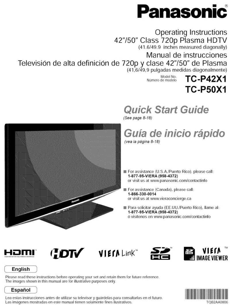
TH-37PE30B / TH-42PE30B
