TABLE OF CONTENTS
1. Specifications ...... . ................... . ...... . ....... . . Page No.
1
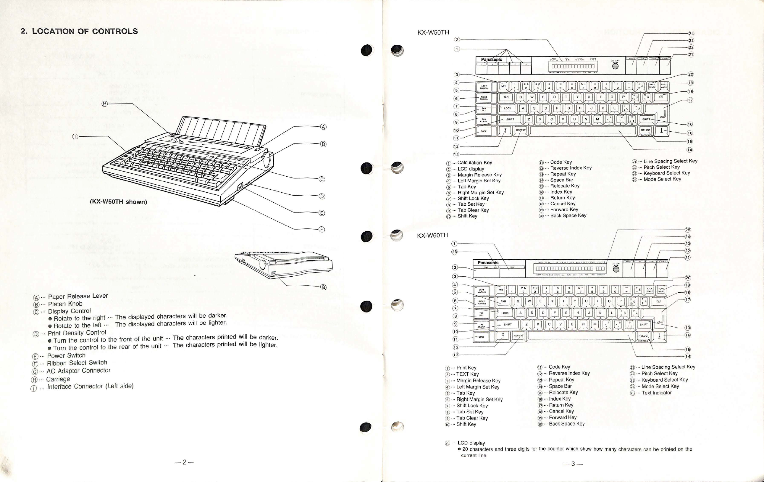
2 . Location of Controls ................. .. ... .... .. ... . . ... .
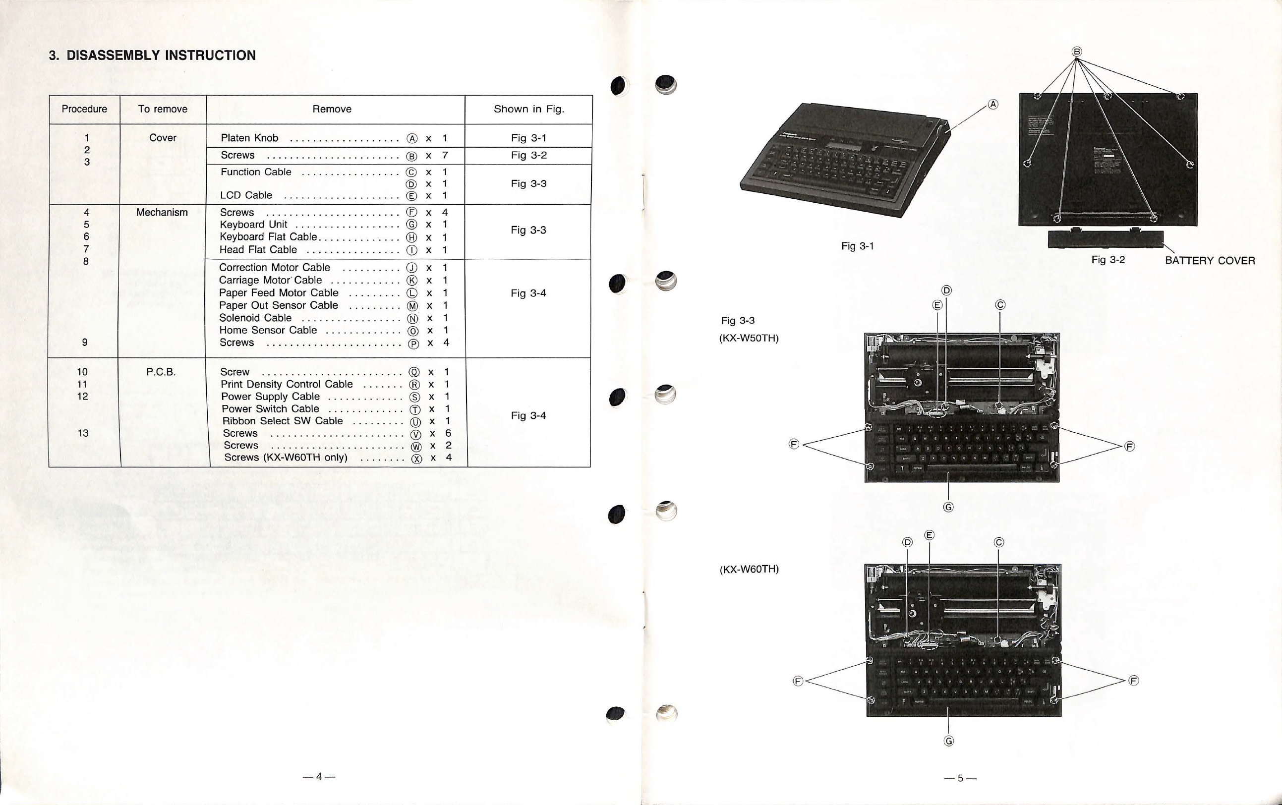
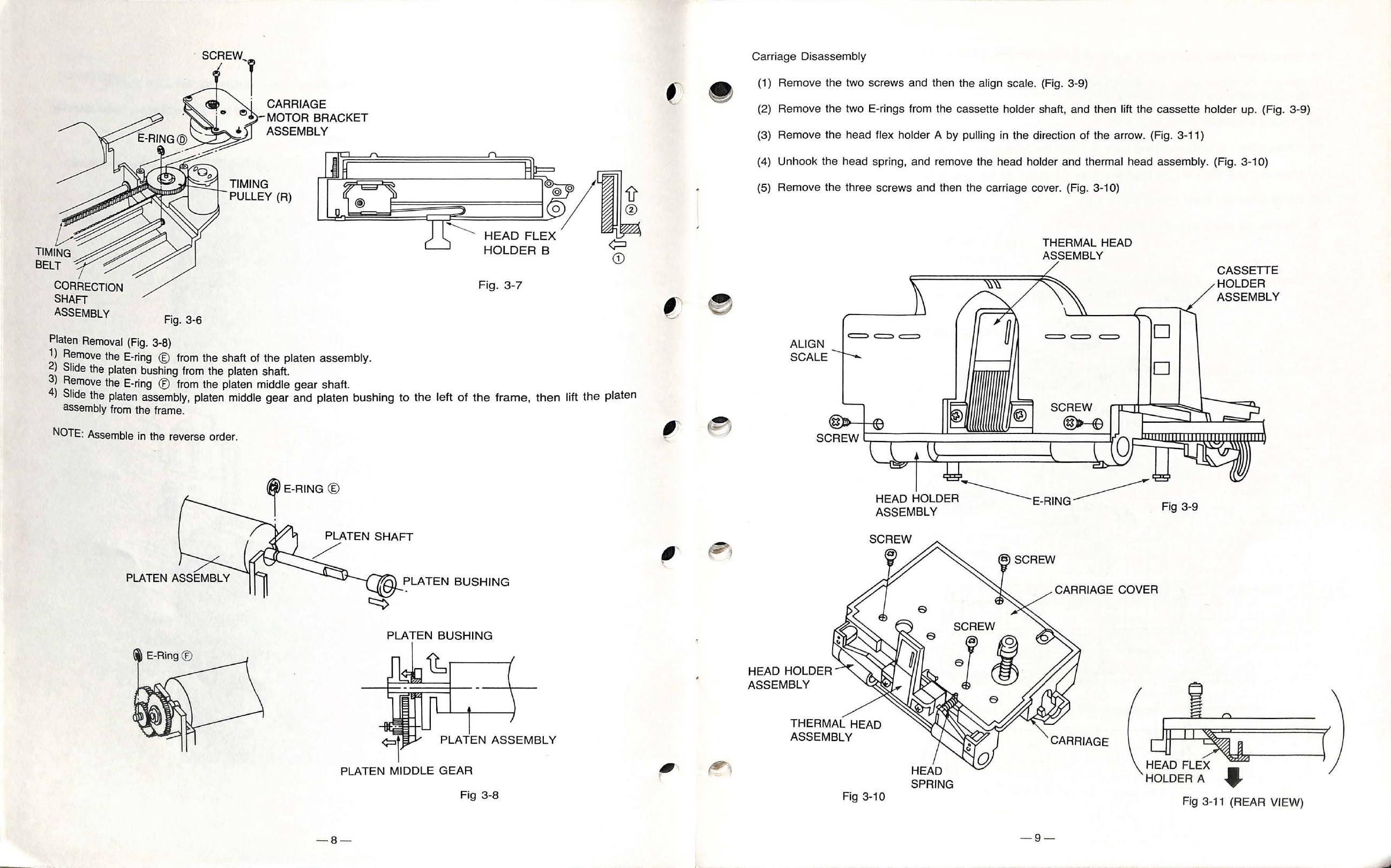
3. Disassembly Instruction ........... .. . . ....... . ....... .. .. .
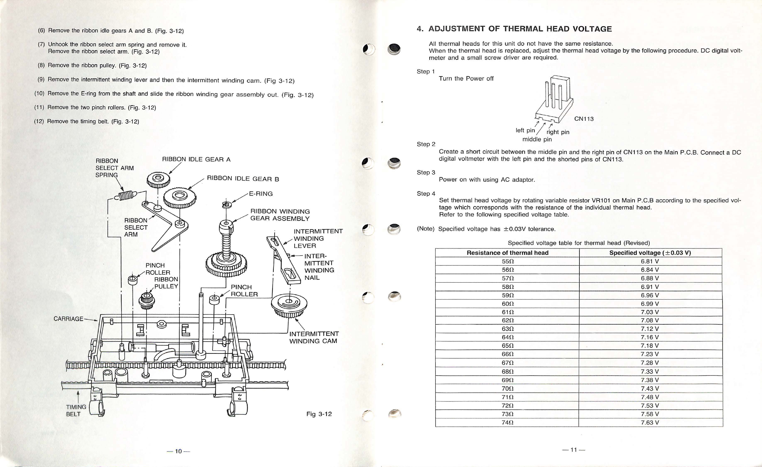
4. Adjustment of Thermal Head Voltage ............ .. . . ... .. .. .
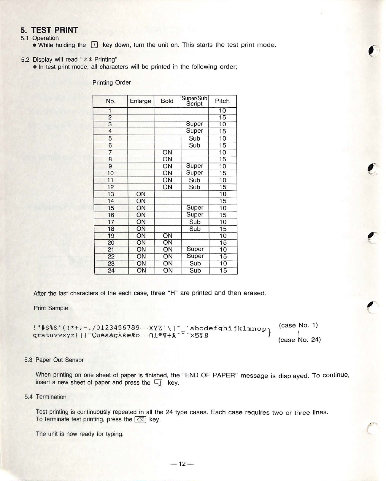
5. Test Print . .. ... .... . ............................ . .... . .
6. Schematic Diagram .. . ........ . ....... . ............ .. ... .
7. Print Circuit Boards .. . ... ............................ .. . .
8. Block Diagram ......... . .... . .......................... .
9. Explanation of Mechanism . ..... ... .......... ... . ..... . .. .
9.1 Printing Section ............................ . . .... . .
9.2 Ribbon Feed Section ... .. .. . .... ...... ..... ... . .... .
9.3 Carriage Spacing Section ... ..................... .
9.4 Paper Feed Section .. .... . . ... . . .. . .... .. .. ... . .... .
10. Explanation of Electronic Operation .. .. ....... ........ ..... .
10.1 Principle of Operation ..... . .. . . .. ... .. . .. . ... . . .. .
10.2 Circuitry . ......... . .. ......... . ... ........ . ... .. .
10.3 Explanation of Connectors . . . . . . . . . . . . . . . . . . . . . . . . . · ·
11. Troubleshooting .. . ..... ... . .......... ... ..... . .. ·. . . · · ·
11.1 Symptoms . . . . . . . . . . . . . . . . . . . . . . . . . . . . . . . . . . . · · · · ·
11.2 Troubleshooting Flow Chart .. ... . . .... .. .... .... : : : :
12. IC Pin Configuration .. . ... . ... ....... ... . .. .. .... .
12.1 Logic Symbol Chart . . . . . . . . . . . . . . . . . ....
.. ..... .. .. . .. .
12.2 Pin Configuration . . . .. .. . ... . .. .. .. .... .. . . .. .... .
13. Parts Location and Parts List ................. ... . .. . . .. .. .
13.1 Covers .... . . .................. ... . ..... . . ..... ....
13.2 Chassis ... . ........ . .. .. . .. .. .. . . .. ..... ..... ...
13.3 Carrier .. . . . ........ .. . . ... . ... ... .... . . . . ... ... .
13.4 Keyboard ... . . . ............... .. . .. .... . .. ... ... .
13.5 Circuit Boards ................... . .. .. .... .
(Main-1/F·DensityControl-RAM Board) .. .. .. ...
13.6 Packing Materials ...... . .................. . .... . . .
2
4
11
12
13
15
17
18
18
19
20
21
22
22
22
41
46
46
49
58
58
58
61
61
64
66
67
70
73
•
•
•
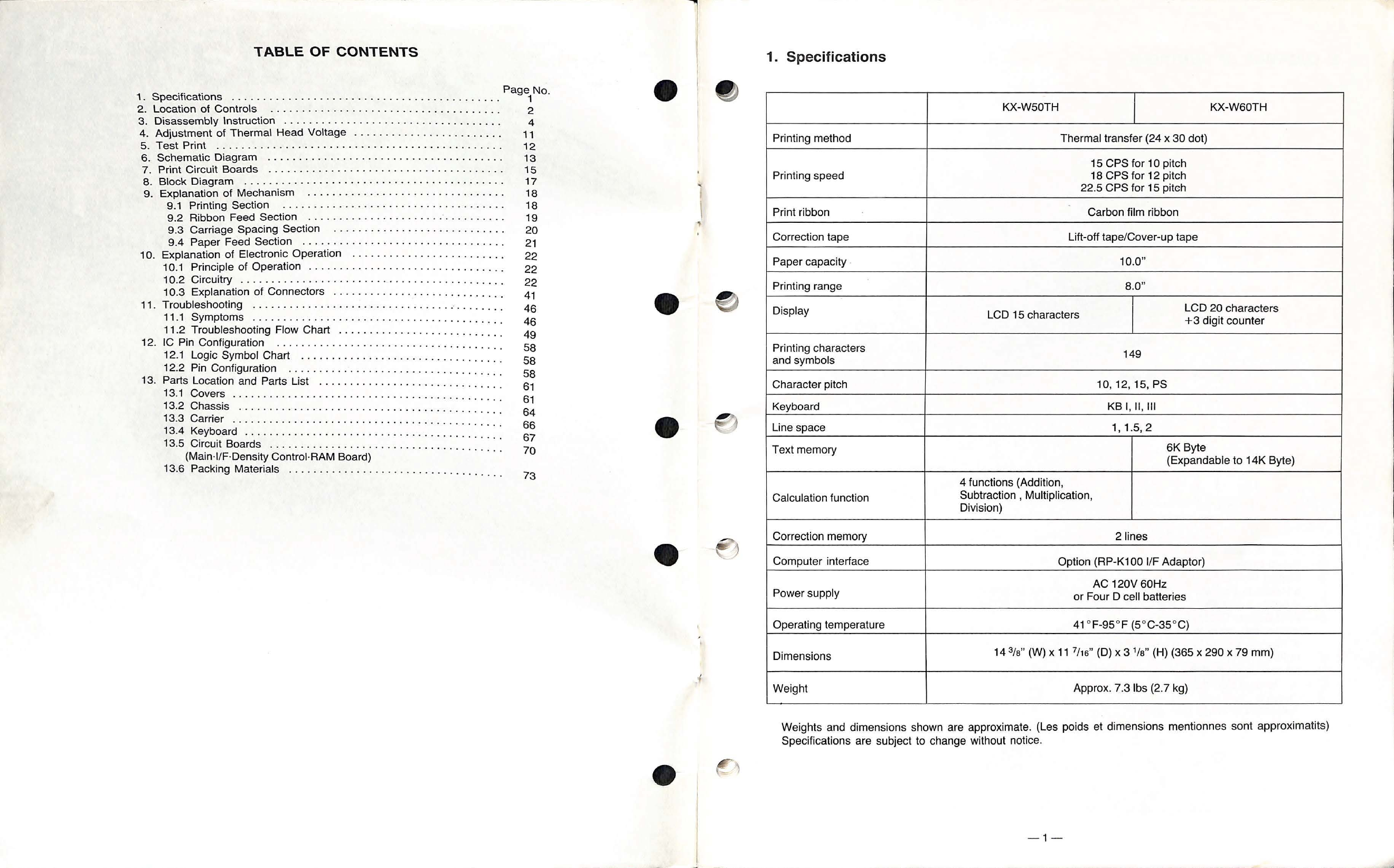
1. Specifications
KX-W50TH KX-W60TH
Printing method Thermal transfer (24 x 30 dot)
15 CPS for 10 pitch
Printing speed 18 CPS for 12 pitch
22.5 CPS for 15 pitch
Print ribbon Carbon film ribbon
Correction tape Lift-off tape/Cover-up tape
Paper capacity 10.0"
Printing range 8.0"
Display LCD 15 characters LCD 20 characters
+3 digit counter
Printing characters 149
and symbols
Character pitch 10, 12, 15, PS
Keyboard KB I, II, Ill
Line space 1, 1.5, 2
Text memory 6K Byte
(Expandable to 14K Byte)
4 functions (Addition,
Calculation function Subtraction , Multiplication,
Division)
Correction memory 2 lines
Computer interface Option (RP-K100 1/F Adaptor )
AC 120V 60Hz
Power supply or Four D cell batteries
Operating temperature 41°F-95°F (5°C-35 °C)
Dimensions 14 3/a"(W)x 11 7/ 16" (D) x 3 1/a" (H) (365 x 290 x 79 mm)
Weight Approx. 7.3 lbs (2.7 kg)
Weights and dimensions shown are approximate. (Les poids et dimensions mentionnes sont approximatits)
Specifications are subject to change without notice.
-1-