For the customer use only
Pericom Semiconductor Corp.
www.pericom.com
Page 3 of 8 9/3/2010
AN 05/05/04
zBoard Circuit
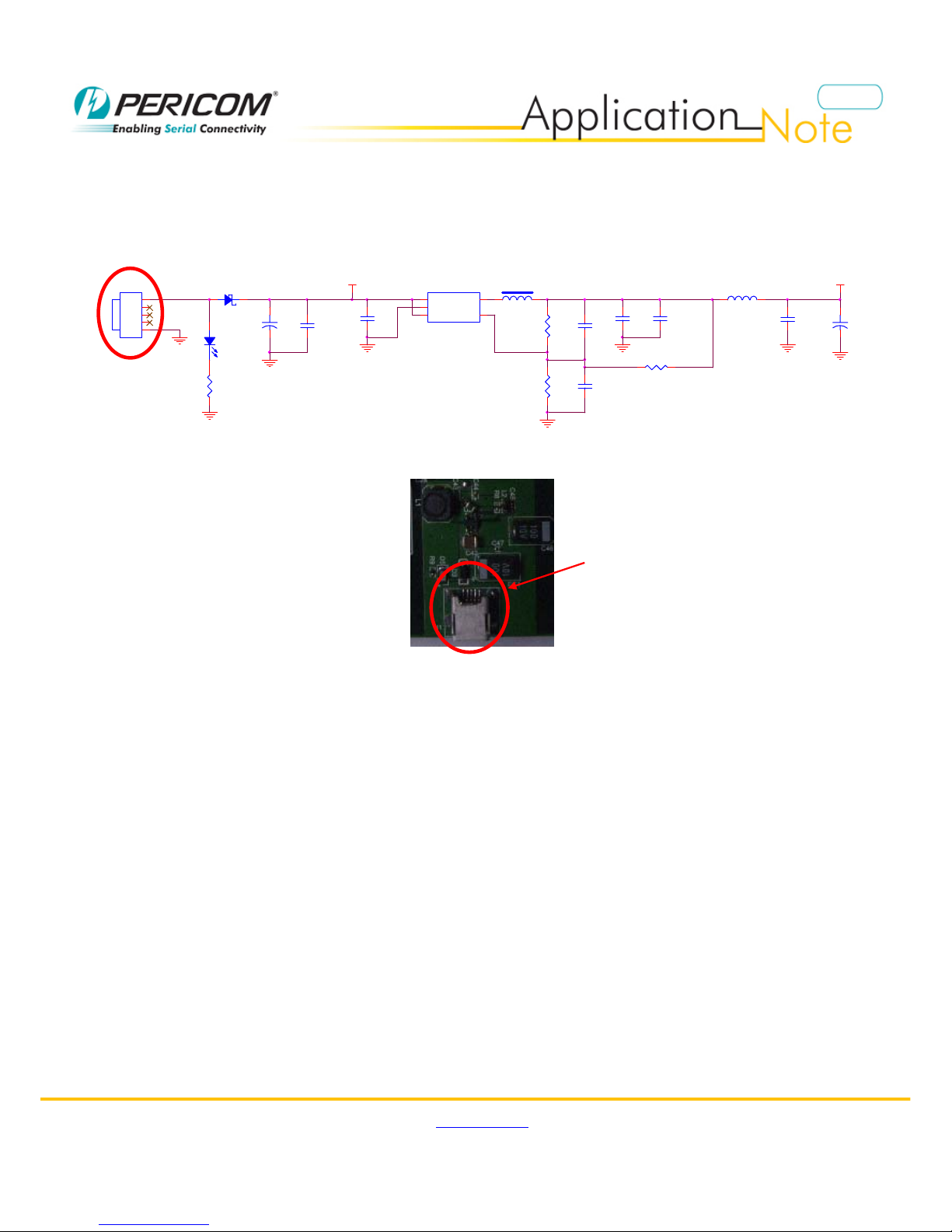
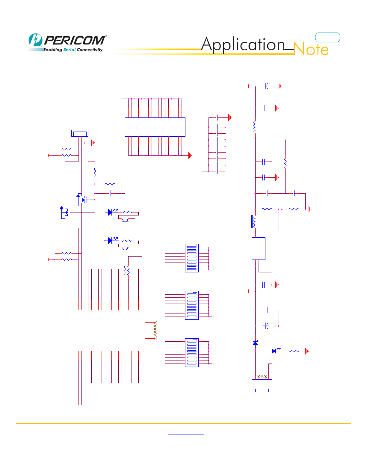
1) Power Supply
On the demo board, the power supply is from one miniUSB connector (J1) by +5V power transforming to +1.2V for
PI2EQX6804-A. Figure3 shows the power circuit.
600mA
+1V2
+
C46100u
U2
LM3674
VIN
1
GND
2
EN
3FB 4
SW 5
R7
280k
J1
Mini USB 2.0 Type B Female
VBUS 1
D- 2
D+ 3
ID 4
GND 5
L1
2.2uH
1 2
R10
200K
C47
0.1u C43
10u C45
0.1u
C42
4.7u C48
12pF
R9
510
D5
LED
12
L2
BL1005LL680
1 2
R8 680K
+
EC1
100uF
12
C49
NP
C44
0.1u
D3
B0520LW
+5.0V
Figure3. Power Circuit for PI2EQX6804-A demo board
Figure4 shows the location for J1.
Figure4. J1 location on PI2EQX6804-A demo board
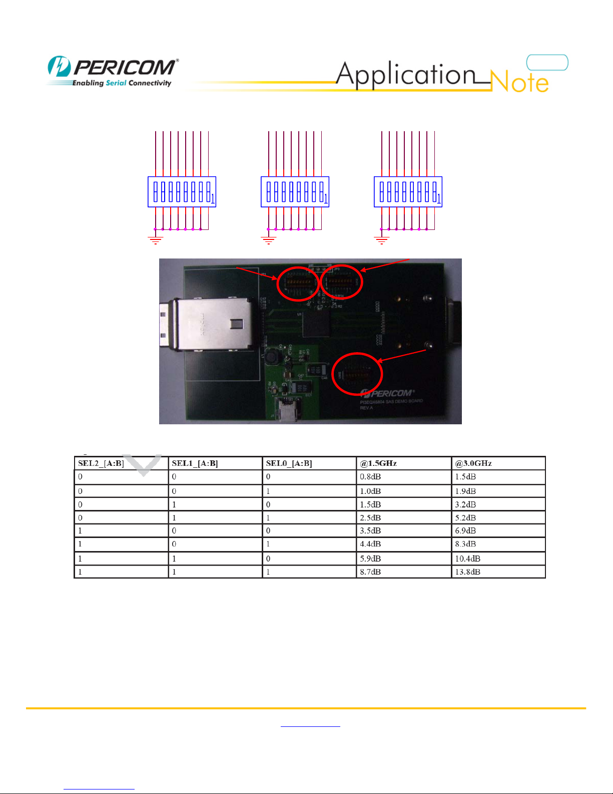
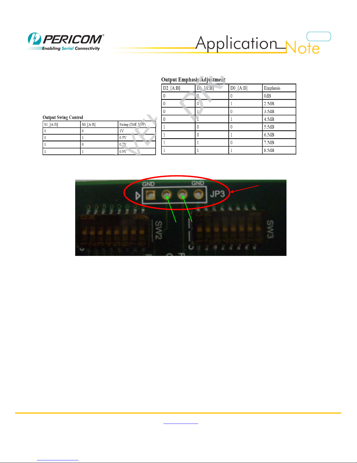
2) Configuration Control
PI2EQX6804-A provides two ways configuration control depending on the state of the MODE input (PIN G5).
MODE determines whether IC configuration status is from the input pins or via I2C control, when MODE is set high,
the configuration input pins set the configuration operating state as stored in configuration registers, changes to these
control registers are disabled and initial condition is protected from any changes to insuring a known operating state.
When MODE pin is low, reprogramming of these control registers via I2C is allowed. NOTE that the MODE pin is not
latched and is always active to enable or disable I2C acces.
During initial power-on, the value at the configuration input pins: LB#, PD#, DE_ [A...B], SEL [0...2] _A, D [0…2] _A,
S0_A, S1_A, SEL [0...2] _B, D [0…2] _B, S0_B, S1_B, will be latched to the configuration registers as initial startup
states. All these pins have internal 100K pull-up resistor.
Figure5 shows the switch and location of these configuration control pins on the demo board.
J1 location


 User manual")


