
Pericom Company Confidential
Pericom Semiconductor Corp.
www.pericom.com
Page 3 of 6 5/24/2011
AN307 05/24
11
#307
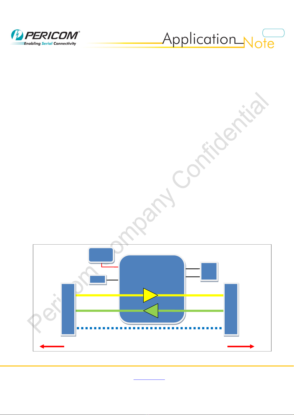
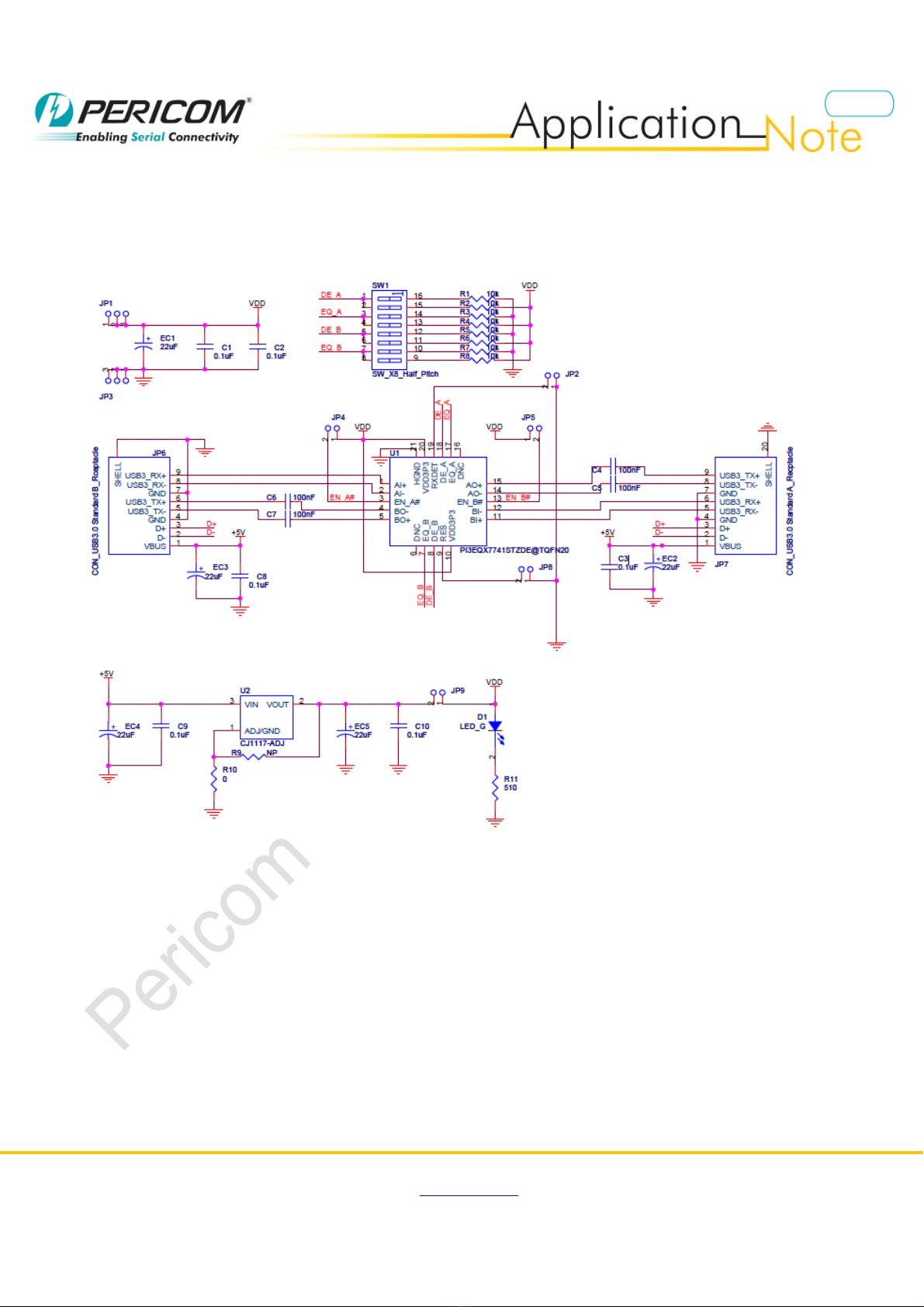
Detail Description
The functionality of header pins of switch are described in this section.
Functionality of Header Pins
Header Pin Header Pin
Name Pins on
PI3EQX7741ST Description
JP2 RxDet RxDet
Short = Receiver detect function disable
Open = Receiver detect function ENABLE
JP4 EN_A# EN_A#
Short = Channel A disable
Open = Channel A ENABLE
JP5 EN_B# EN_B#
Short = Channel B disable
Open = Channel B ENABLE
JP8 VTH* RES Reserved pin – MUST tie HIGH for normal operation
JP9 VDD VDD33
Short = Use internal power
Open = Use external 3.3V power
VTH* is connected to RES pin on PI3EQX7741ST
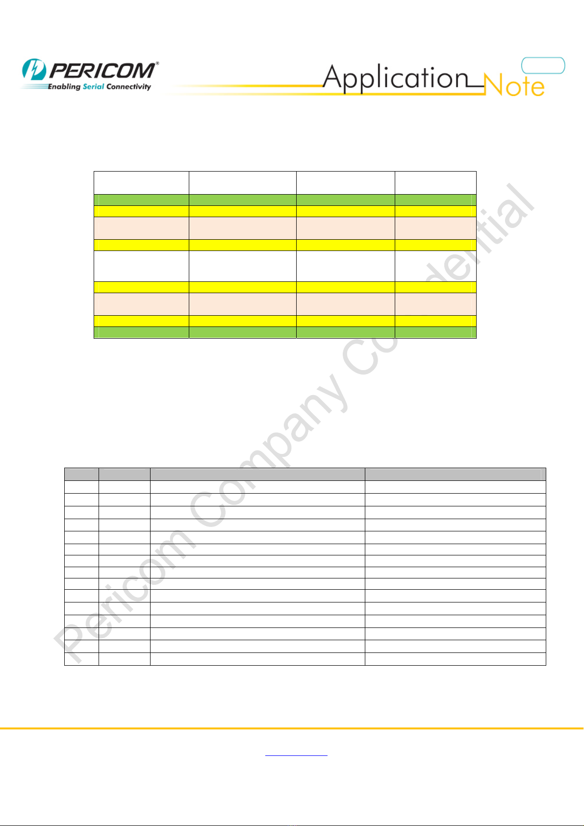
Functionality of Switch (SW1)
Switch - # Pin on
PI3EQX7741ST Switch Status Value
SW1 – 1 = ON, SW1 – 2 = OFF 0dB
SW1 – 1 = OFF, SW1 – 2 = OFF -3.5dB
SW1 – 1
SW1 – 2 DE_A
SW1 – 1 = OFF, SW1 – 2 = ON -6dB
SW1 – 3 = ON, SW1 – 4 = OFF 3dB
SW1 – 3 = OFF, SW1 – 4 = OFF 6dB
SW1 – 3
SW1 – 4 EQ_A
SW1 – 3 = OFF, SW1 – 4 = ON 9dB
SW1 – 5 = ON, SW1 – 6 = OFF 0dB
SW1 – 5 = OFF, SW1 – 6 = OFF -3.5dB
SW1 – 5
SW1 – 6 DE_B
SW1 – 5 = OFF, SW1 – 6 = ON -6dB
SW1 – 7 = ON, SW1 – 8 = OFF 3dB
SW1 – 7 = OFF, SW1 – 8 = OFF 6dB
SW1 – 7
SW1 – 8 EQ_B
SW1 – 7 = OFF, SW1 – 8 = ON 9dB


 User manual")


