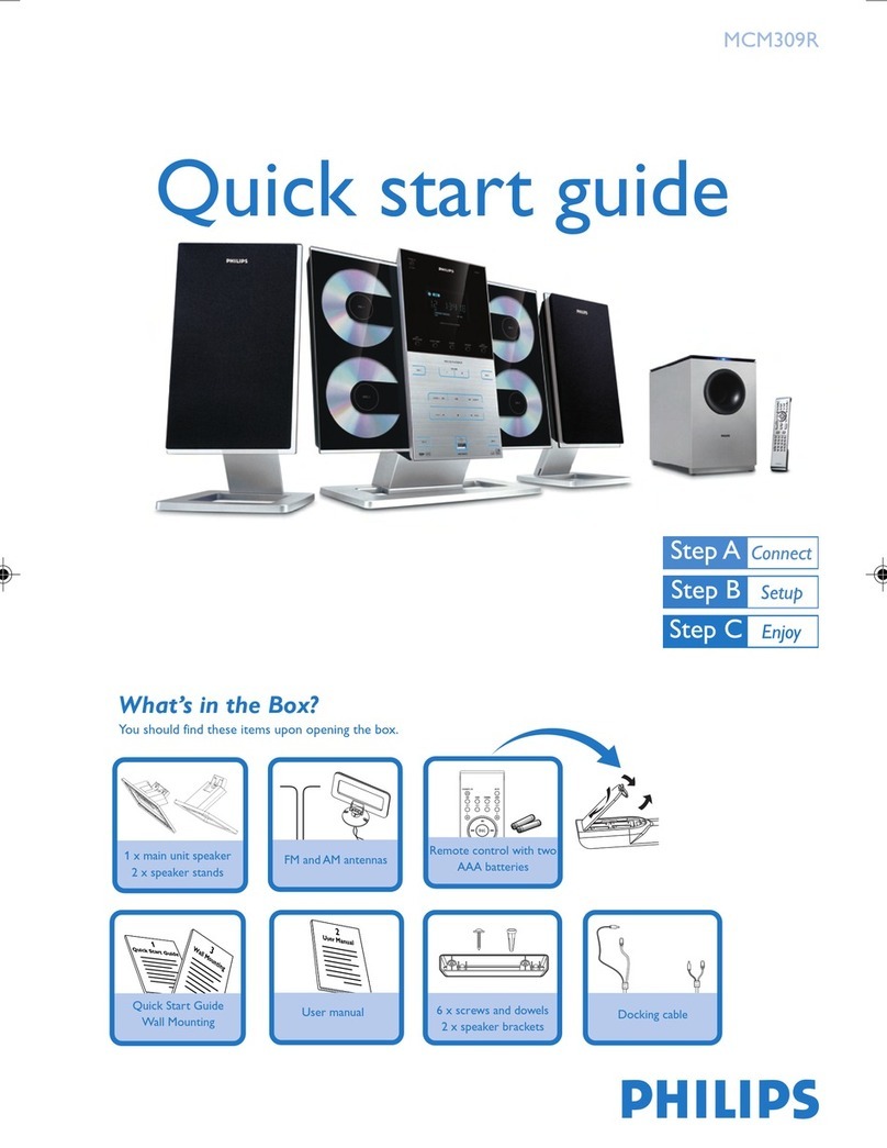
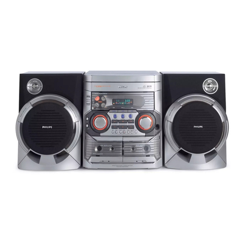
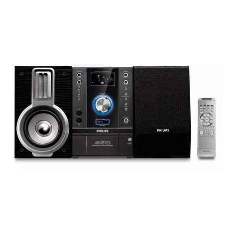
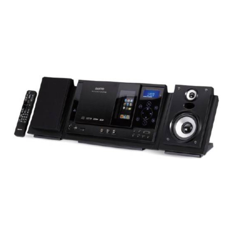
Philips DCM713 User manual

CD Micro System
TABLE OF CONTENTS
3141 785 34330
XL 09 08
2008
Location of PC Boards .................................................... 1-1
Electronic Specification
................................................... 1-2
Measurement Setup ....................................................... 1-3
Service Aids ................................................................... 1-4
Items Of Safety Attention ......................................1-5 to 1-6
Instruction On CD Playability .................................1-7 to 1-8
Software Version Check & Upgrade .............................. 2-1
Malfuction Check Chart .................................................. 3-1
Disassembly Diagram ...................................................4-1
Block Diagram ................................................................. 5-1
Wiring Diagram................................................................. 6-1
Decoder Board .................................................................10
Circuit diagram ............................................. 10-1 to 10-4
Layout diagram ....................................................... 10-5
Power Board .....................................................................11
Circuit diagram ............................................. 11-1 to 11-2
Layout diagram ......................................................... 11-3
VFD Display Board .............................................................7
Circuit diagram ........................................................... 7-1
Layout diagram ........................................................... 7-2
USB & Headphone Board ....................................................8
Circuit diagram ........................................................... 8-1
Layout diagram ........................................................... 8-1
Ipod Docking Board .............................................................9
Circuit diagram ........................................................... 9-1
Layout diagram ........................................................... 9-1
Exploded View ...............................................................12-1
Service Parts List .............................................. 13-1 to 13-2
Factory Parts List .............................................. 14-1 to 14-4
DCM713
5HFRUGDEOH
5H:ULWDEOH

Location of PC Boards
VERSION VARIATIONS :
Type /Versions:
Features
Board in used:
DCM713
Service policy
Ipod Docking Board
Hearphone Board
Power Board
USB Board
CD Loader Mechanism
Decoder Board
Speaker Output Board
VFD Display Board
* TIPS : C -- Component Lever Repair.
M -- Module Lever Repair
-- Used
/55
/55
/58
/58
/61
/61
/79
/79
/93
/93
/94
/94
/96
/96
/98
/98
/51
/37
/12
/12
/05
/05
Feature diffrence
RDS
TDS
VOLTAGE SELECTOR
ECO STANDBY - DARK
M
C
C
C
C
M
C
M
Type /Versions:
DCM713
Ipod Docking
Board
Hearphone Board
Decoder Board
VFD Display Board
AMP Power Board
CD Loader
Driver
USB Board
Speaker Output
Board
1-1

1-2
Electronic Specification
AMPLIFIER
Rated Output Power ........................... 2 x 50 RMS
6LJQDOWRQRLVHUDWLRG%$e
)UHTXHQF\UHVSRQVH+]a.+]G%
Aux Input ................................. 0.5V RMS 20kohm
DISC
Laser Type ..................................... Semiconductor
Disc Diameter ........................................ 12cm/8cm
Support Disc .......................................... CD-DA,
CD-R,CD-RW,MP3-CD,WMA-CD
$XGLR'$&%LWVN+]
Total Harmonic Distortion .................˘0.1%(1kHz)
Frequency Response ........................ 20Hz~20kHz
6LJQDOWR1RLVH5DWLRG%$
TUNER
)07XQLQJ5DQJH0+]
Tuning grid .................................................. 50KHz
Sensitivity
- MRQRGE615DWLR ............................ ˘G%I
±6WHUHRGE615DWLR˚G%I
Selectivity .................................................. ˚G%I
,PDJH5HMHFWLRQG%
Total Harmonic Distortion ................ ˘0.1%(1kHz)
6LJQDOWR1RLVH5DWLRQG%$
SPEAKERS
Speaker Impedance ................................................ 4 ohme..
6SHDNHU'ULYHUEDVH´
6SHDNHU'ULYHUWZHHWHU´r
)UHTXHQF\5HVSRQVH+].+]
GENERAL INFORMATION
Total Output power ......................................... 100W RMS
AC Power ........................................................ 230V/50Hz..
Operation Power Consumption ............................... 100W
6WDQGE\3RZHU&RQVXPSWLRQ:
(FR6WDQGE\3RZHU&RQVXPSWLRQ:
Headphone Output .......................................................1W
86%'LUHFW9HUVLRQ)6
Dimensions
–0DLQXQLWZ[K[G[[PP
–6SHDNHUER[Z[K[G[[PP
–6XEZRRIHUZ[K[G1$
Weight
–With Packing ...................................................... 10.5KGP
–Main unit ..............................................................1.82KG
–6SHDNHUER[[.*
–6XEZRRIHU1$
Specifications and external appearance are
VXEMHFWWRFKDQJHZLWKRXWQRWLFH

1-3
LF Generator
e.g. PM5110
Recorder
Use Universal Test Cassette CrO2 SBC419 4822 397 30069
LEVEL METER
e.g. Sennheiser UPM550
with FF-filter
with FF-filter
S/N and distortion met
e.g. Sound Technology ST170
L
R
DUT
or Universal Test Cassette Fe SBC420 4822 397 30071
LEVEL METER
e.g. Sennheiser UPM550
S/N and distortion meter
e.g. Sound Technology ST1700B
L
R
DUT
CD
Use Audio Signal Disc
(replaces test disc 3) SBC429 4822 397 30184
Bandpass
250Hz-15kHz
e.g. 7122 707 48001
LF Voltmeter
e.g. PM2534
DUT
S/N and distortion meter
e.g. Sound Technology ST1700B
Frame aerial
e.g. 7122 707 89001
Tuner AM (MW,LW)
To avoid atmospheric interference all AM-measurements have to be carried out in a Faraday´s cage.
Use a bandpass filter (or at least a high pass filter with 250Hz) to eliminate hum (50Hz, 100Hz).
RF Generator
e.g. PM5326
05=iR
Bandpass
250Hz-15kHz
e.g. 7122 707 48001
LF Voltmeter
e.g. PM2534
DUT
RF Generator
e.g. PM5326
S/N and distortion meter
e.g. Sound Technology ST1700B
Use a bandpass filter to eliminate hum (50Hz, 100Hz) and disturbance from the pilottone (19kHz, 38kHz).
05=
i
R
Tuner FM
Measurement Setup

1-4
INFORMATION ABOUT LEAD-FREE SOLDERING
GB WARNING
All ICs and many other semi-conductors are
susceptible to electrostatic discharges (ESD).
Careless handling during repair can reduce life
drastically.
When repairing, make sure that you are
connected with the same potential as the mass
of the set via a wrist wrap with resistance.
Keep components and tools also at this
potential.
ESD
CLASS 1
LASER PRODUCT
GB
Safety regulations require that the set be restored to its original
condition and that parts which are identical with those specified,
be used
Safety components are marked by the symbol
Philips CE is producing lead-free sets from 1.1.2005 onwards.
Regardless of special logo(not always indicated) one must treat all sets from onwards,according next rules:
IDENTIFICATION:
!.
Lead free
1 Jan 2005
Service Aids

tems of Safety Attention
1-5
Attention: Please read tems of Safty Attention carefully. f
there are une pected conflicts between safefy attention and
maintenance attention, please abide to safety attention Safety
first.
C M A
Before operating, please unplug the AC power cord from the
outlet.
a) Disassemble any parts.
b) Cut-off or re-connect plug and other inserting parts.
c) hen electrolysis capacitance and test parts is parallel
connected, anti-polarity and wrong replace will cause
e plosion.
Do not spray chemical on the component system, surroundings
and any parts.
Clean the electric unction with a cotton stick which is with
cleaning mi ture, e cept there is other demand in this manual.
P :
t is a kind of inflammable mi ture.
Do not use lubricant to the soldering point, e cept there is
other demand in this manual
C C
During maintenance, please take common controlling to protect
component system and electronic parts and prevent damages
to the circuit due to improper operation.
Led out wire should be kept away from high-pressure or
high-temperature parts.
ES
Some semi-conductor parts are easily damaged by static
charges, these parts are called ES. They are mainly the cores
of transistor lead identification. The following technical ways
can be used to reduce the damages by static charges.
Before connecting semi-conductor or the parts. Let off the
static charges of the body by connection the earth. n the other
hand, to prevent potential electric shock hazard, please use
industrial static handle before connecting power for checking
the e uipment.
After unsoldering the ES parts, put the parts on a electric
surface such as aluminum foil to prevent accumulating static
charges to damage the parts.
nly use anti-static charges grounded soldering irons to
unsolder the parts or solder ES parts.
Some soldering tin called Anti-static charges can also
generate charges to damage ES parts.
Do not use poisonous and caustic agent which these kinds of
chemicals can generate static charges to damage the ES
parts.
Do not take ES parts out of conductive packages until they are
used (mostly replacing ES parts is packed with aluminum foil or
similar conductive materials making a short circuit).
After taking replaceable ES parts from Anti-static charges
cone, please insert the ES parts in the correctly location soon
as possible.
During handing sealed ES parts, reduce the movement of the
body (clothes rubbing and moving on the rug can generate
static charge to damage the ES parts.)
M A C S R
Use only grounded low-voltage soldering iron, and proper size and
shape which can sustain the temperature of soldering horn to
range from 350 to 390.
Use rosin flu which is demanded by RMA include 60 Tin 40
lead.
To maintain soldering iron and its tin very well.
Use the wire brush but not spray cleaners such as Freon to clean
the soldering surface.
Adopt the melting ways
a) The temperature of soldering horn range from 350 to 390.
b) Heat up the parts pin, until soldering tin is molten.
c) Use the desoldering pump to suck out the molten soldering tin
uickly.
N:uickly operating can prevent superheating the
electronic-plating copper.
Adopt the following soldering ways.
a) The temperature of soldering horn range from 350 to 390.
b) Hold the soldering iron and welding rod pointed to the parts pin,
until soldering tin is molten. Then move the soldering horn
uickly to the location that you want to solder.
N:uickly operating can prevent superheating
electronic-plating copper of printed circuit board.
c) Check the welting zone carefully, then brush the unwanted
soldering tin away with a wire brush.
URIC
N:
Do not touch the C body directly with soldering iron.
Pre-heating soldering iron at about 130 for some seconds avoid
the damages caused by C heated suddenly.
For normal C, the temperature of the solder horn is about 350,
and can increase to 390 for some bigger C.
Use the filamentous welding rod and solder which thickness is
about 0.3mm to solder thin C and add the solder as needed.
Replace the C carefully and solder it uickly.
After unsoldering the C, clean the basic board carefully to ensure
the board is usable.
Prevent the molten soldering tin dripping on the board which will
engender a short circuit.
Aim at the first terminal and fi it, then aim at other terminals for
correctly inserting C. ou can solder uickly ust like this.
Before operating, please make sure the C is unusable. Do not
unsolder repeatedly.
During soldering especially soldering a thin C with many pins,
check the weld carefully.
After replacing, check that there is not soldering leak, rosin oint,
short circuit and so on.
U:
Use the soldering iron to melt the soldering tin.
Before unsoldering C, suck out the molten solder tin.
R˖
Make sure all the C pins are on their correct location, then solder.
Use a wire brush to clean the welting zone.


Items of Safety Attention
1-6
Unsolder/replace diode
After unsoldering the unusable diode, nip its body and take it
out.
Bend the two pins and the diode is vertical to circuit board.
Check the polarity of the diode, then place its pins to the
correct location.
Pin the joint and solder it.
Check the weld carefully. If the surface of the weld is not
smooth, please solder it again.
Repair electro-plating copper
Repair the warpage copper as following:
Use a sharp knife to scrape the unusable copper and the
unwanted solder off.
Make one side of the lead bent like a small “U”, then put the
“U” to IC pins and solder. Another side of the lead is extended
until overlap with the well copper then solder. Cut the unwand
lead.
The flow of repairing DVD part
No sound or sound distorted when playing, please check the
DVD part.
Notes for taking down the laser head
Before operating, read these notes as following to prevent the
static charges damageing the laser head when reading the
laser led.
Lay an electric rug on the working table and the replaced parts
are packed in black package.
The electric rug is grounding by put on the electric base.
Then put your hand on the electric rug and connect the static
handle with the electric rug. Make sure the electric rug and the
working table are grounding.
During the operating, do something such as operating on the
electric rug to avoid the static charges touching the laser parts.
After that, you can begin to take the laser parts down.
When replace the laser parts, please do something to make a
short circuit and remenber to cut the short circuit off after
replacing.

6HWUHPDLQVFORVHG
1
<
3OD\D&'
IRUDWOHDVWPLQXWHV
<
SOD\DELOLW\
RN"
1
SOD\DELOLW\
RN"
DGG,QIRIRUFXVWRPHU
6(72.
FKHFNSOD\DELOLW\
1
<
SOD\DELOLW\
RN"
FKHFNSOD\DELOLW\
FKHFNSOD\DELOLW\
UHWXUQVHW
&XVWRPHUFRPSODLQW
&'UHODWHGSUREOHP
IDVWOHQVFOHDQLQJ
)RUIODSORDGHUV DFFHVVWR&'GULYHSRVVLEOH
FOHDQLQJPHWKRGLVUHFRPPHQGHG
([FKDQJH&'0
)RUGHVFULSWLRQVHHIROORZLQJSDJHV
,QVWUXFWLRQ2Q&'3OD\DELOLW\

3/$<$%,/,7<&+(&.
)RUVHWVZKLFKDUHFRPSDWLEOHZLWK&'5: GLVFV
XVH&'5:3ULQWHG$XGLR'LVF
75)LQJHUSULQW
75 %ODFNGRWPD[LPXPDW
SOD\EDFNRIWKHVHWZRWUDFNVZLWKRXWDXGLEOHGLVWXUEDQFH
SOD\LQJWLPHIRU )LQJHUSULQW VHFRQGV
%ODFNGRWIURPWR
MXPSIRUZDUGEDFNZDUGVHDUFKZLWKLQDUHDVRQDEOHWLPH
)RUDOORWKHUVHWV
XVH&''$6%&$
75 %ODFNGRWPD[LPXPDW
75)LQJHUSULQW
75 ZHGJH
SOD\EDFNRIDOOWKHVHWUDFNVZLWKRXWDXGLEOHGLVWXUEDQFH
SOD\LQJWLPHIRU ZHGJH VHFRQGV
)LQJHUSULQW VHFRQGV
%ODFNGRWIURPWR
MXPSIRUZDUGEDFNZDUGVHDUFKZLWKLQDUHDVRQDEOHWLPH
&86720(5,1)250$7,21
,WLVSURSRVHGWRDGGDQDGGHQGXPVKHHWWRWKHVHWZKLFK
LQIRUPVWKHFXVWRPHUWKDWWKHVHWKDVEHHQFKHFNHG
FDUHIXOO\EXWQRIDXOWZDVIRXQG
7KHSUREOHPZDVREYLRXVO\FDXVHGE\DVFUDWFKHGGLUW\RU
FRS\SURWHFWHG&',QFDVHSUREOHPVUHPDLQWKHFXVWRPHU
LVUHTXHVWHGWRFRQWDFWWKHZRUNVKRSGLUHFWO\
7KHOHQVFOHDQLQJPHWKRGVKRXOGEHPHQWLRQHGLQWKH
DGGHQGXPVKHHW
7KHILQDO ZRUGLQJ LQ QDWLRQDO ODQJXDJH DV ZHOO DVWKH SULQWLQJ
LV XQGHU UHVSRQVLELOLW\RIWKH 5HJLRQDO6HUYLFH2UJDQL]DWLRQV
/,48,'/(16 &/($1,1*
%HFDXVHWKHPDWHULDORIWKHOHQVLVV\QWKHWLFDQGFRDWHG
ZLWKDVSHFLDODQWLUHIOHFWLYLW\OD\HUFOHDQLQJPXVWEHGRQH
ZLWKDQRQDJJUHVVLYHFOHDQLQJIOXLG,WLVDGYLVHGWRXVH
³&OHDQLQJ6ROYHQW
7KHDFWXDWRULVDYHU\SUHFLVHPHFKDQLFDOFRPSRQHQWDQG
PD\QRWEHGDPDJHGLQRUGHUWRJXDUDQWHHLWVIXOOIXQFWLRQ
&OHDQWKHOHQVJHQWO\GRQ¶WSUHVVWRRKDUGZLWKDVRIWDQG
FOHDQFRWWRQEXGPRLVWHQHGZLWKWKHVSHFLDOOHQVFOHDQHU
7KHGLUHFWLRQRIFOHDQLQJPXVWEHLQWKHZD\DVLQGLFDWHGLQ
WKHSLFWXUHEHORZ
%HIRUHWRXFKLQJWKHOHQVLWLVDGYLVHGWRFOHDQWKH
VXUIDFHRIWKHOHQVE\EORZLQJFOHDQDLURYHULW
7KLVWRDYRLGWKDWOLWWOHSDUWLFOHVPDNHVFUDWFKHVRQ
WKHOHQV
,QVWUXFWLRQ2Q&'3OD\DELOLW\

2-1
Software Version Check & Upgrade
Upgrade software
Software version and date check
1. Download the software from Philips support website
2. Insert the USB device or DISC with the Software.
3. VFD Display :
READING
PRESS OK
http://www.philips.com/support
Wating for about a few minutes
Input the “966” figure on Remote Control
Press the “ Display ” key on Remote Control
UPGRADING
UPGRADE OK
1. Select USB station, VDF Display:
READ USB
DCM713 Vxx
YYMMDD

Not power
Check the Power Cord
is connected
Check whether the
PowerBoard has provided
voltage output
Not sound
Confirm that whether turn
on the TV’s volume
Check if the Main Board
has been provided voltage
Don’t display
Check the files or folders in
USB or other devices do not
exceed the certain limit
Not picture on HDMI connection
Check if the HDMI cable
is usable
Replace a new
HDMI cable
Check the connect cable is
OK or NOT
Check the flat connect wire is
OK or NOT and Re-planted
Check if the data wire which
connected to the Main Board
has been provided voltage
Check the data wire which
connected the Main Board,
if has provided voltage
Check if the Transistors
have been provided voltage
Check the Digital Output
Board whether provide voltage
Check if the CPU IC
has provided voltage
Check if the VFD Board
has been provided voltage
Replace a new
Power Board
N
Replace a
new one
N
Replace a
new one
N
Replace a
new one
N
Replace the IC PT6311
/SC16311/CD16311
N
N
Replace the
Main Board
N
Change to ues
the new materials
N
Change to
uesable one
N
Check if the Main Board
has provided voltage
Replace a
new one
N
Y
Y
Y
Y
Y
Don’t Loading
Confirm that the Loader
Mechanism has provided
Voltage
Check the Flat Loader
cable is OK or NOT
Check the flat connect wire is
OK or NOT and Re-planted
Check the Loader whether
has provided Voltage
Replace a
new one
N
Replace a
new one
N
Replace a
new one
N
Y
Y
Y
Y
Y
Y
Y
Y
Y
Y
Malfunction Follow Check Chart
3-1 3-1

Disassembly Diagram
4-1
4-1
A. Loose these Claspers to remove
the DVD Door
B. Remove the Back Cabinet
B1 B2
D. Remove the Volume KnobC. Remove Front Cabinet
C1. Loose 3pcs screws(3 x 8 FT)
B1. Loose 8pcs screws(3 x 8 FT)
B2. Loose 3pcs screws(3 x 10 FA)
E. Loose 8pcs screws(3 x 8 PA) G. Loose 3pcs screws(3 x 8 BA)
H. Loose 1pc screw(3 x 10 BTH)
I. Remove the Ipod Docking Seating
I. Use the Clincher to mover the Fixer Axis
Pull Direction Pull Direction
E
GH
C1
H.Remove the CD Loader Driver
Mechanism
G. Remove the Dusctproof Cover
E. Remove the Display Board

5-1 5-1
Block Diagram
MCU5V
-24V
VF1 VF2
VFD Driver
VFD
KEY
IR
AMC1117
AMC1117
M3.3V
M1.8V
AC110-220
22V
3.3V
1.8V
POWER SUPPLY
8 Ohm 50W at 10%
FR SPK
8Ohm50Wat10%
FL SPK
PT16311
M5V MCU5V
VFD
VF2
VF1 POWER
-27V SUPPLY
AMPLIFIER BOARD FL TRE
19mm cloth dome
FR TRE
19mm cloth dome
ECO_POWER
1
2
1
2
TDA8947
POWER AMP
22V
BTL
L+
R+
FL
FR
Main chipset
ZR36966XD
Loader motor driver
CD5888
M5V
SDRAM
SERIAL FLASH
M3.3V
M3.3V
MCU5V
IR
MP3 LINE IN
FM Antenna 75OHM
AUX1
USB
MCU R5F21266
FM
Si4704
MCU5V
M5V
K4S161622C-TC/L70
1M
Open/Close Driver
M5V
Door Detect
DISPLAY BOARD
MAIN BOARD
or Si4705(RDS)
MCU I2C
M3.3V
FM RST
F4558
PWM->
15V
AUDIO ML/MR
MCU5V
FM RST
STANDBY
ECO_POWER
MPEG I2C
4052 A,B
M3.3V
M1.8V
M5V
EEPROM
M3.3V
AT24C02
1M * 16
AT26DF081A
IPOD-DIN9
74LV4052
SWITCH
M5V
PCM1808
ADC
M5V
IIS BUS
4052 A,B
ANL-AUDIO
M1.8V
HEAD PHONE
MUTE
STANDBY
MUTE
DM-06BXLX-L2
Foryou pick up
DVD Loader
CLOSE DOOR
OPEN DOOR
FL
FR
FL
FR
5V
STANDBY
MCU5V
MUTESTADBY
PT2309
5V
5V
22V
STANDBY
15V
15V
MUTE
STANDBY
5V
22V
IR
IR
IR
MCU5V
ECO_POWER
MCU5V
VFD I2C
ipod L/R

6-1 6-1
Wiring Diagram

7-1
7-1
VFD Display Board -- Circuit Diagram
SW1
1
SW2
2
SW3
3
SW4
4
DOUT
5
DIN
6
IC
7
CLK
8
STB
9
KEY1
10
KEY2
11
KEY3
12
KEY4
13
Vdd 14
S1/KS1 15
S2/KS2 16
S3/KS3 17
S4/KS4 18
S5/KS5 19
S6/KS6 20
S7/KS7 21
S8/KS8 22
S9/KS9 23
S10/KS10 24
S11/KS11 25
S12/KS12 26
S13 27
S14 28
S15 29
S16 30
S17/G12 31
S18/G11 32
Vdd 33
VEE 34
S19/G10 35
S20/G9 36
G8 37
G7 38
G6 39
G5
40
G4
41
G3
42
G2
43
G1
44
Vdd
45
LED5
46
LED4(BBE)
47
LED3(POWER)
48
LED2(FANCT)
49
LED1(7507RST)
50
Vss
51
OSC
52
IC301
PT6311
R314 47K
R307 33K
R308 33K
R309 33K
R310 33K
K4
K3
K2
K1
D304 4148
D305 4148
VFD STB
VFD CLK
VFD DATA
S1
S2
S3
S4
S5
S6
S7
S8
S9
KS1
KS2
-24V
S1
S2
R306
2.2R 1/2W
VF1
VF2
S10
S11
S12
S13
S14
S15
S16
S17
S18
G10
G1
G2
G3
G4
G5
G6
G7
G8
G9
R305 2.2R 1/2W
C310
47uF
R312
4K7
R311
10K R313
10K
G1
G2
G3
G4
G5
G6
G7
G10
S2
S1
S3
S4
S5
S6
S7
G9
S9
S10
S11
S12
S13
G8
S15
S14
S16
SW303
FUNCTION SW304
STOP
SW308
OPEN/CLOSE
SW302
MODE
SW305
PREVIOUS
SW306
PLAY/PAUSE
SW307
STANDBY
S8
S17
VF1
2
NC
3
NC
4
NC
5
NC
6
G1
7
G2
8
G3
9
G4
10
G5
11
G6
12
G7
13
G8
14
G9
15
G10
16
NC
17
NC
18
S1
19
S2
20
S3
21
S4
22
S5
23
S6
24
S7
25
S8
26
S9
27
S10
28
S13
31
VF1
1
S14
32
S11
29
S12
30
S15
33
S16
34
S17
35
NC
36
NC
37
NC
38
VF2
39
VF2
40
VFD301DCM713D-1.GB
+5V
1
2
3
4
5
6
7
8
9
10
CN301
10P/2.0
+5V
V-GND
REM
ROT-A
ROT-B
R322
4.7k
LED301
REM
1
GND
2
Vcc
3
S301
REMOTE
REM
V-GND
+5V
+5V
C309
104p
ECO POWER
1
2
10
9
7
6
3
4
5
T902
BZ1
L305
200UH
Q301
D965
Q302
D965
R319 1K
R320 1K
R378 100
C308 104p
C307
220U/35V
D301 FR104 -24V
R381
100
R379
100
DZ301 3V
C301
104M
VF1
VF2
D302
4148
ECO POWER
R315
10k
R316
15
DZ302
27v
G
1B
2A
3
ENCODER301
ENCODER
ROT-A1
ROT-B1
R301 10K
R302
10K
R304
10K
R303
10K
+5V
C302
103P
C303
103P
ROT-A
ROT-B
V-GND
VFD CLK
VFD DATA
VFD STB
C304
220P
C305
220P
C306
220P
R321
47
C312
47uf/16v
C311
104p

7-2
7-2
VFD Display Board -- Layout Diagram

8-1 8-1
USB & Headphone Board -- Circuit & Layout Diagram
1
2
3
4
CN401
GND-u
D+
D-
vbus
1
2
3
CN501
3P/2.0
J202C
J502A
J202B
3
2
1
J501
SP-2JCK
AUX-L
AUX-R
GND-1
HP-L-1
HP-R-1
PH-MUTE-1
1
2
3
4
CN502
4P/2.0
vbus 5
D- 2
D+ 3
GND 4
GND 1
J401
USB HOST

9-1
9-1
Ipod Docking Board -- Circuit Diagram
R201 1K
R203 1K
C202
102
DGND
+5V
RX
TX
RCH_IPOD
LCH_IPOD
SSDA/TX
SSCL/RX
+5V
AGND
IPOD_DET C203
102
C201
470/10
1
2
3
4
5
6
7
8
9
CN201
9P/2.0
R208 0GND
1
GND
2
Right
3
Left
4
Right In
5
Left In
6
7
Video Out
8
9
10
GND
11
Rx
12
Tx
13
14
GND
15
GND
16
17
3.3V
18
+12V
19
+12V
20
Serial enable
21
TPA(-)
22
5VDC(+)
23
TPA(+)
24
Data(-)
25
TPB(-)
26
Data(+)
27
TPB(+)
28
GND
30 GND
29
GND
31
GND
32
GND
33
GND
34
GND
35
GND
36
37
37
CN202
30P-IP
R213
49.9K
R211
75k
R210
75k
R212
49.9K
DGND
R215
549k
R229 100
R230 100
R202(NC)
0
L201
FB 2.2KU
VCC DET
C204
104P
R204
22K R205
22K
R206 0
R207 0

9-2
9-2
Ipod Docking Board -- Layout Diagram

10-110-1
Decoder Board -- Circuit Diagram
Vaddis-966XE
Use it to connect the shell of the crystal with ground.
Close to Vaddis!
Important power s upply!
500mA for device
RESET
Crystal
Put at the middle of traces.
Close to pin 38
ICETMS
USB
External 2ch Audio DAC amd ADC
Close to Va ddis!
XXmA
3.30V
For EMI (As Close as possible to U100 )
Serial Flash pinout - for reference
JP100 JP101
Release
Download
Debug
Pin1-2 short
Pin2-3 short
Pin1-2 short
Open
Pin2-3 short
Pin1-2 short
Close to
Vaddis
OSCIN
IPCLK
GP-3 AIN
DRVSB
CD_DVD
SFCS
SFDO
SFDI
SFCLK
USB_DP
USB_DN USB_DN1
USB_DP1
VDDPLL
SFDI_0
VC
LD_DVD
MD_DVD
RAMADD9
SFCS_0
RFP
RESOUT
RFN
RAMDAT11
RAMADD3
RAMADD4
OSCIN
RAMDAT2
RAMDAT3
RAMDAT8
HOMESW
VDDPWM
RAMWE-
RAMCS0-
RAMADD10
LD_CD
RAMDAT9
IPCLK
RAMADD6
VDDDAC
RAMDAT13
RAMBA
RAMADD5
VDDDAC
RAMADD0
VDDAFE
DSPVCC18
VDDAFE
INSW
SFCLK_0
RESET#
RAMDAT0
RAMDAT12
RAMDAT10
RAMDAT6
RAMDQM
RAMCAS-
RAMRAS-
VDDPWM
RAMDAT1
RAMADD7
RAMADD1
VDDAFE
SPDL_PWM
RAMADD8
SFDO_0
VDDAFE
TRACK_PWM
RF_C
RESET#
VDDPLL
DRVSB
IPOD-RX
RAMDAT7
SPDL_SENS-
SPDL_SENS+
MD_CD
SLED_PWM
IRRCV
OSCOUT
RAMDAT14
RAMDAT4
RAMDAT5
RAMADD2
CD_DVD_1
FOCUS_PWM
PCLKPCLK
SDRAM3.3V
DSPVCC33IDSPVCC33I
RAMCKE
INSW-CPUINSW
SFDO
SFDI
SFCLK
SF_CS
USB_DP
USB_DN
GP-0
GP-3
GP-5
HOMESW
SFCS
VREF
OSCOUT
RF
RF_F
RF_E
RF_A
RF_B
RF_D
GP-0
GP-4
K
L
CC2
I
T
A
D
C
2I
RAMDAT15
S/PDIF_OUT
C_B_U
Y_R_V
CVBS_C
CVBS_G_Y
VDDDAC
SF_CS
GP-4
RAMCAS-
RAMCKE
RAMADD8
RAMDAT5
RAMDAT4
RAMDAT15
RAMDAT9
RAMADD4
RAMDQM
RAMADD7
RAMWE-
RAMADD0
RAMADD9
RAMDAT7
SDRAM3.3V
RAMADD10
RAMADD1
RAMADD2
RAMDAT11
RAMCS0-
RAMDAT6
RAMDAT0
RAMDQM
RAMADD5
RAMADD6
RAMDAT10
RAMDAT2
RAMRAS-
RAMDAT1
RAMBA
RAMDAT13
RAMDAT12
RAMADD11
RAMADD3
PCLK
RAMCS1-
RAMDAT8
RAMDAT14
RAMDAT3
RAMBA
RAMDQM
RAMADD5
RAMADD6
RAMRAS-
PCLK
RAMDAT0
RAMDAT11
RAMADD3
RAMCS0-
RAMDAT1
RAMDAT12
RAMDAT13
RAMDAT4
RAMDAT10
RAMCKE
RAMDAT2
RAMCAS-
RAMDAT3
RAMADD1
RAMDAT14
RAMDAT8
RAMDAT15
RAMDAT9
RAMADD7
RAMADD10
RAMDAT7
RAMWE-
RAMADD9
RAMDAT5
RAMADD4
RAMADD0
RAMDQM
RAMADD8
RAMADD2
RAMDAT6
SDRAM3.3V
RAMADD11
RAMCS1-
VDDAFE
GP-0
GP-5
DRVSB
HOMESW
ABCLK
ALRCLK
AMCLK
RF
CD_DVD
RF_C
IPOD-TX
MD_DVD
SPDL_PWM
LD_CD
LD_DVD
SLED_PWM
TRACK_PWM
MD_CD
FOCUS_PWM
SPDL_SENS-
VC
RF_B
RF_A
RF_F
SPDL_SENS+
IPOD-RX
RF_D
RF_E
APWM_L-
AIN
I2CCLK
APWM_R-
S/PDIF_OUT
Y_R_V
CVBS_C
CVBS_G_Y
C_B_U
I2CDAT
FM-RST
MUTE_CTL
IPOD-RST
INSW-CPU
DSPVCC33
DSPVCC33
DSPVCC18
DSPVCC18
DSPVCC33
DSPVCC33
DSPVCC33
DSPVCC18
VDDAPWM
DSPVCC33I
DSPVCC33
SDRAM3.3V
DSPVCC33
DSPVCC33
+5V
DSPVCC33
DSPVCC33
DSPVCC33
R16
392 Ohm 1%
C39
10nF
C43
0.1uF
FB19 MBW2012-1K
C9 22pF
R30 27R
C37
10nF
FB28 FB/2K
R27 100R
C128
100pF
C36
10nF
U7
NM
K4S641632H-UC70]
1
2
3
4
5
6
7
8
9
10
11
12
13
14
15
16
17
18
19
20
21
22
23
24
25
26
27 28
29
30
31
32
33
34
35
36
37
38
39
40
41
42
43
44
45
46
47
48
49
50
51
52
53
54
VDD
DQ0
VDDQ
DQ1
DQ2
VSSQ
DQ3
DQ4
VDDQ
DQ5
DQ6
VSSQ
DQ7
VDD
DQML
WE#
CAS#
RAS#
CS#
BA0
BA1
A10
A0
A1
A2
A3
VDD VSS
A4
A5
A6
A7
A8
A9
A11
NC
CKE
CLK
DQMH
NC
VSS
DQ8
VDDQ
DQ9
DQ10
VSSQ
DQ11
DQ12
VDDQ
DQ13
DQ14
VSSQ
DQ15
VSS
R15 33R
Y1
27.000MHz
+
EC23
100uF/10V
C11
10nF
U1
MX25L1605D
1
2
3
45
6
7
8
/CS
SO
/WP
GND SI
SCK
/HOLD
VDD
C47
10nF
FB29 FB/2K
PH1 1
.
C12
10nF
R117 100R
FB6 MBW2012-221
C1
10nF
R4 15.4K(1%)
C25
1nF
C134
100pF
C40
10nF
+
EC5
100uF/10V
FB7
MBW2012-221
C52
10nF
U2A
ZR36966
102
101
93
92
91
90
86
84
87
85
82
83
81
88
89
70
80
72
76
77
74
75
71
68
69
73
67
66
103
104
105
106
107
108
109
124
123
125
126
127
1
2
3
4
5
7
6
8
10
9
11
13
14
15
16
12
17
18
20
19
21
23
22
24
25
27
26
28
29
32
30
33
34
35
65
64
63
62
61
60
59
58
56
55
54
53
52
57
51
50
49
48
46
45
44
43
42
41
40
39
38
119
120
121
122
31
36
37
110
111
112
113
114
115
116
118
117
78
79
128
100
99
98
97
96
95
94
47
Gen_5/GPIO[0]
Gen_6
GPIO[52]/PWMCO[3]/HSYNC
GPIO[51]/PWMCO[2]/FIELD
GPIO[50]/PWMCO[1]/VCLKx2
VDDPWM
DVD_MD
VDDSAFE
CD_LD
CD_MD
RESOUT
GNDREF
VREF
DVD_LD
GPIO[49]/PWMCO[0]
B
VC
C
K
F
J
E
VDDAFE
VDD1AFE
A
D
RFN
RFP
Gen_4/VID7
SFCS
GND
SFDO/RS_SF
SFDI/RS128_Bootsel2
VDDC
VDDP
RAMADD[6]
RAMADD[2]
RAMADD[1]
RAMADD[7]
VDDC
RAMADD[0]
RAMADD[8]
RAMADD[10]
VDDP
RAMADD[9]
RAMCS0#
RAMADD[11]/GPO[64]
RAMBA
RAMRAS#
RAMCS1#/GPO[65]
RAMCAS#
RAMWE#
RAMDQM
GNDPCLK
PCLK
VDDP
VDDPCLK
RAMDAT[8]
RAMDAT[9]
RAMDAT[7]
RAMDAT[6]
RAMDAT[5]
RAMDAT[10]
RAMDAT[11]
RAMDAT[4]
RAMDAT[3]
RAMDAT[12]
VDDIP
RAMDAT[13]
RAMDAT[14]
RAMDAT[2]
RAMDAT[1]
RAMDAT[15]
RAMDAT[0]
GNDDACBS2
RSET
DAC1
VDDDAC
DAC2
DAC3
VDDDAC
DAC4
XIN
XO
VDDPLL
GNDPLL
RESET#
GNDC
VDDC
VDDP
IGPIO[44]
GPIO[43]/DUPRD0/TDO/SSCTXD
GPIO[32]/SPDIFO
VDDP
GPIO[29]/AMCLK/APWM0-
GPIO[28]/APWM1-
GPIO[26]/APWM2-
GPIO[25]/AOUT2/APWM3-
GPIO[24]/DUPRD1/ALRCLK/APWM4-
IGPIO[23]/DUPTD1/ABCLK/APWM5-
VDDAPWM
RAMADD[4]
RAMADD[3]
RAMADD[5]
VDDIP
VDDC
VDDP
GNDAPWM
SFCLK/RS128_Bootsel1
GPIO[5]
SD_D/IGPIO[7]
PWM5
SD_CMD/GPIO[6]
SD_CLK/IGPIO[7]
VDDP
DN
DP
VFE_YIN
GND1AFE
GND
VDDP
Gen_7
Gen_8
Gen_9
Gen_11
Gen_12/VID0
VDDC
GND
C38
10nF
TP28
R17 33R
C27
0.1uF
C8
1nF
C16 0.1uF
C85
10pF
FB2
MBW2012-221
C22 10nF
C13 1nF
R25
10K
C28
0.1uF
R10 4.7K
FB27 MBW2012-1K
+
EC111
220uF/6.3V
R28
56R
C29
56pF
C14 1nF
R145 75R1%
R2
220K
C21 100pF
C31
0.1uF
R18 33R
C49
10nF
C30
56pF
R5
1K
U3
K4S161622C-TC/L70
1
2
3
4
5
6
7
8
9
10
11
12
13
14
15
16
17
18
19
20
21
22
23
24
25
50
49
48
47
46
45
44
43
42
41
40
39
38
37
36
35
34
33
32
31
30
29
28
27
26
VDD
DQ0
DQ1
VSSQ
DQ2
DQ3
VDDQ
DQ4
DQ5
VSSQ
DQ6
DQ7
VDDQ
LDQM
WE
CAS
RAS
CS
BA
A10/AP
A0
A1
A2
A3
VDD
VSS
DQ15
DQ14
VSSQ
DQ13
DQ12
VDDQ
DQ11
DQ10
VSSQ
DQ9
DQ8
VDDQ
NC
UDQM
CLK
CKE
NC
A9
A8
A7
A6
A5
A4
VSS
R148 75R1%
R7 220R
C35
10nF
C45
10nF
R12 4.7K
R3 1K
C42
10nF
C4
1nF
C20
1nF
R150 75R1%
R115
10K
FB8
MBW2012-221
C32
10nF
C41
10nF
R32
15K
C2 22pF
+
EC1
22uF/16V
C15
33pF
C51
10nF
C96
10nF
R37
10K
+
EC2
220uF/6.3V
TP27
FB1
MBW2012-221
C19
1nF
R21 100R
FB3
MBW2012-221
+
EC3
100uF/10V
C34
10nF
FB4
MBW2012-221
R1 75R
R152 75R1%
R116
10K
R31
15K
R29 27R
CN1
2.0-4P
1
2
3
4
R9
4.7K
R14 33R
FB5
Table of contents
Other Philips Stereo System manuals

Philips
Philips MC260 User manual

Philips
Philips MCM190/21 User manual

Philips
Philips FW-C85 User manual

Philips
Philips FW8/25 User manual

Philips
Philips MCM1055 User manual

Philips
Philips DCD2030/93 User manual

Philips
Philips FW390 Quick start guide

Philips
Philips FW-C579 User manual

Philips
Philips MC 135 User manual

Philips
Philips FW-C28 User manual

Philips
Philips MCM240 User manual

Philips
Philips FWM390/21 User manual

Philips
Philips MCM166/12 User manual

Philips
Philips FWM400D/12 User manual

Philips
Philips FWD410/98 User manual

Philips
Philips FW-C380 User manual

Philips
Philips FW-V355 User manual

Philips
Philips FWM462X/78 User manual

Philips
Philips DCM2060 User manual

Philips
Philips FW34 User manual