manuals.online logo
Brands
  1. Home
  2. •
  3. Brands
  4. •
  5. Philips
  6. •
  7. Stereo System
  8. •
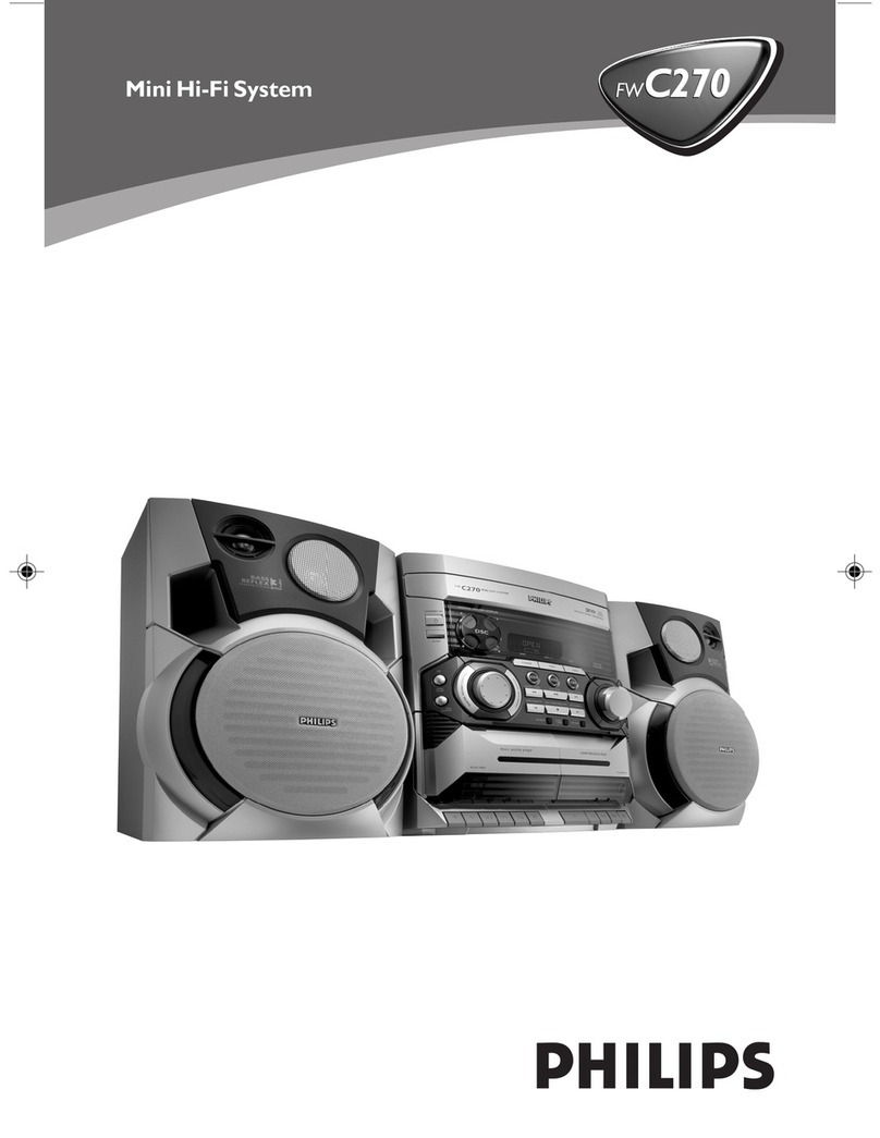
  9. Philips FW-C355/21 User manual

Philips FW-C355/21 User manual

This manual suits for next models

2

Other Philips Stereo System manuals

Philips MCM159/98 User manual

Philips

Philips MCM159/98 User manual

Philips BM60B/10 User manual

Philips

Philips BM60B/10 User manual

Philips FW-C10 User manual

Philips

Philips FW-C10 User manual

Philips MC-M250 User manual

Philips

Philips MC-M250 User manual

Philips FW-V28 User manual

Philips

Philips FW-V28 User manual

Philips FWD573/98 Operating manual

Philips

Philips FWD573/98 Operating manual

Philips FW-C90 User manual

Philips

Philips FW-C90 User manual

Philips FWC555 User manual

Philips

Philips FWC555 User manual

Philips F 880 User manual

Philips

Philips F 880 User manual

Philips SBCHC790/00 User manual

Philips

Philips SBCHC790/00 User manual

Philips AZ329/98 User manual

Philips

Philips AZ329/98 User manual

Philips Streamium WMS8080/12 User manual

Philips

Philips Streamium WMS8080/12 User manual

Philips MCM330/12 User manual

Philips

Philips MCM330/12 User manual

Philips MCM155 User manual

Philips

Philips MCM155 User manual

Philips FWD186 User manual

Philips

Philips FWD186 User manual

Philips FW 326 User manual

Philips

Philips FW 326 User manual

Philips MCM238/12 User manual

Philips

Philips MCM238/12 User manual

Philips Streamium MCI500H/05 User manual

Philips

Philips Streamium MCI500H/05 User manual

Philips MCD280/30 Operating manual

Philips

Philips MCD280/30 Operating manual

Philips Magnavox FW 48 User manual

Philips

Philips Magnavox FW 48 User manual

Philips FW930P2/2 User manual

Philips

Philips FW930P2/2 User manual

Philips MC165 User manual

Philips

Philips MC165 User manual

Philips MC138 series User manual

Philips

Philips MC138 series User manual

Philips AZ 2407 User manual

Philips

Philips AZ 2407 User manual

Popular Stereo System manuals by other brands

Sony HCD-VX88 Service manual

Sony

Sony HCD-VX88 Service manual

Sony CMT-SPZ90DB operating instructions

Sony

Sony CMT-SPZ90DB operating instructions

LG OM4560 owner's manual

LG

LG OM4560 owner's manual

JVC UX-G3 instructions

JVC

JVC UX-G3 instructions

Odys ODYS - LOOP instruction manual

Odys

Odys ODYS - LOOP instruction manual

Aiwa NSX-AJ700 Service manual

Aiwa

Aiwa NSX-AJ700 Service manual

Panasonic SC-AK100 operating instructions

Panasonic

Panasonic SC-AK100 operating instructions

Sharp CD-G10000V Operation manual

Sharp

Sharp CD-G10000V Operation manual

Bogen NEARSCAPES 4.1 manual

Bogen

Bogen NEARSCAPES 4.1 manual

Panasonic SCPM29 - MINI HES W/CD PLAYER operating instructions

Panasonic

Panasonic SCPM29 - MINI HES W/CD PLAYER operating instructions

Meyer LD-3 operating instructions

Meyer

Meyer LD-3 operating instructions

THOMSON MIC302U manual

THOMSON

THOMSON MIC302U manual

Sony SS-CEP50 Service manual

Sony

Sony SS-CEP50 Service manual

Cetacea Sound CVS-II user guide

Cetacea Sound

Cetacea Sound CVS-II user guide

Sony MHC-V21D Service manual

Sony

Sony MHC-V21D Service manual

Denon UCD-250 Service manual

Denon

Denon UCD-250 Service manual

Exibel BDX600-UK user manual

Exibel

Exibel BDX600-UK user manual

Sanyo DC-F320 Service manual

Sanyo

Sanyo DC-F320 Service manual

manuals.online logo
manuals.online logoBrands
  • About & Mission
  • Contact us
  • Privacy Policy
  • Terms and Conditions

Copyright 2025 Manuals.Online. All Rights Reserved.

CLASS 1
LASER PRODUCT
COMPACT
DIGITAL AUDIO
ServiceManual
Service
Service
Service
Service
Service
FW-C355/21/22/34
TABLE OF CONTENTS
Page
Location of pc boards & Version variations ................1-2
Technical Specifications .............................................1-3
Measurement setup ....................................................1-4
Service Aids, Safety Instruction, etc...........................1-5
Disassembly Instructions & Service positions .............. 2
Service Test Programs & DEMO mode ......................... 3
Set Block diagram ......................................................... 4
Set Wiring diagram ........................................................ 5
Front Board .................................................................... 6
Mains Board................................................................... 8
ETF7 Tape Module ........................................................ 9
3CDC-LLC-MCD1 Module ........................................... 10
Combi Board ................................................................ 11
Set Mechanical Exploded view & parts list ................. 12
©Copyright 2002 Philips Consumer Electronics B.V. Eindhoven, The Netherlands
All rights reserved. No part of this publication may be reproduced, stored in a retrieval system or
transmitted, in any form or by any means, electronic, mechanical, photocopying, or otherwise
without the prior permission of Philips.
Published by KC 0203 Service Audio Printed in The Netherlands Subject to modification
GB
3139 785 30028
Mini System
Version 1.0
3-1 3-1
Various
other Tests
Activated with ACTION
TEST
QEEPROM FORMAT Load default data. Display shows "NEW"
for 1 second.
Caution!
All presets from the customer will be lost!!
Disconnect
mains cord
LEAVE SERVICE
TESTPROGRAM
R
9to Exit
EEPROM TEST A test pattern will be sent to the EEPROM.
"PASS" is displayed if the uProcessor read
back the test pattern correctly, otherwise
"FAIL" will be displayed.
Volume Knob
or
Jog Shuttle knob
ROTARY
ENCODER TEST Display shows value for 2 seconds.
Values increases or decreases in steps of 1
until 0 (Min.) or 40 (Max.) is reached.
DBBDEMO DEMO will toggle on or off.
The message: "DEMO ON" or "DEMO OFF"
will scroll across the display to show the
new status of the set.
STANDBY-ON
Button pressed?
Y
N
Set is in Service PLAY Mode.
The Service Play Mode is intended to
detect and identify the failures in the CD Mode.
In this mode the electronics will still function
even when an error is detected so that
repair activities can be carried out.
SERVICE
PLAY MODE
In case of failures, error
codes according to table 2
will be displayed.
O
Button pressed?
Y
Y
Y
N
N
N
O
Button pressed?
9
Button pressed?
Display shows
8M
Output at (Front Board)
pin 80 of uP = 1,953.125Hz
Display shows
32K
Output at (Front Board)
pin 80 of uP = 2048Hz
QUARTZ
TEST
Note: During the 3CDC tray may "jerks" open
& close or the carousel may rotates
slightly. This is due to sharing of control
lines during the Service test program.
TUNER
Button pressed?
Disconnect
Mains cord ?
Y
N
N
Y
Service frequencies are
copied to the RAM (see Table1)
Tuner works normally
except:
PROGRAM button
Service Mode left
TUNER
TEST
Display Tuner Version
"ccc"
TUNER
Button pressed?
N
Y
PRESET
1
2
3
4
5
6
7
8
9
10
11
Europe
"EUR"
87.5MHz
108MHz
531kHz
1602kHz
558kHz
1494kHz
87.5MHz
87.5MHz
87.5MHz
87.5MHz
98MHz
East Eur.
"EAS"
87.5MHz
108MHz
531kHz
1602kHz
558kHz
1494kHz
87.5MHz
87.5MHz
87.5MHz
87.5MHz
98MHz
USA
"USA"
87.5MHz
108MHz
530kHz
1700kHz
560kHz
1500kHz
98MHz
87.5MHz
87.5MHz
87.5MHz
87.5MHz
Oversea
"OSE"
87.5MHz
108MHz
530/531kHz*
1700/1602kHz*
560/558kHz*
1500/1494kHz*
98/87.5MHz*
87.5MHz
87.5MHz
87.5MHz
87.5/98MHz*
Table 1
East Eur. Extended-band
"EAS"
65.81MHz
108MHz
74MHz
87.5MHz
531kHz
1602kHz
558kHz
1494kHz
98MHz
70.01MHz
65.81MHz
Note: * Depending on the selected grid frequency (9 or 10kHz)
By holding the TUNER and R buttons depressed while switching on the Mains supply, one
of the undermentioned features will be activated:
- the tuning grid frequency is toggled between 9kHz and 10kHz for the Oversea (/21) version.
- the extended FM1 (65.81MHz - 74MHz) is toggled on and off for East Eur. (/34) version.
Y
N
Y
N
Y
N
DIM
Button pressed?
DIM
Button pressed?
9
Button pressed?
DISPLAY
TEST
Display shows Fig. 2
and selected LEDs on
(see note 2)
Display shows Fig. 1
and selected LEDs on
(see note 1)
Figure 1
Figure 2
note 2 : OPTIMAL is on while JAZZ & TECHNO are off, other LEDs status
are not important (applicable only for sets with LEDs)
note 1 : JAZZ & TECHNO are on while OPTIMAL is off, other LEDs status
are not important (applicable only for sets with LEDs)
Table 2
Error code
E1000
E1001
E1002
E1003
E1005
E1006
E1007
E1008
E1020
E1070
E1071
E1079
Error Description
Focus Error
Triggered when the focus could not be found within a certain time when starting up the CD
or when the focus is lost for a certain time during play.
Radial Error
Triggered when the radial servo is off-track for a certain time during play.
Sledge In Error
The sledge did not reach its inner position (inner-switch is still close) before approximately
6 Sec. have passed by. Inner-switch or sledge motor problem.
Sledge Out Error
The sledge did not come out of its inner position (inner-switch is still open) before approximately
250 mSec. have passed by. Inner-switch or sledge motor problem.
Jump-offtrack error
Triggered in normal play when the jump destination could not be found within a certain time.
When this error occurred, software will try to recover by initiating the jump command again.
If it is recoverable, the disc will continue to play.
Subcode Error
Triggered when a new subcode was missing for a certain time during play.
PLL Error
The Phase Lock Loop could not lock within a certain time.
Turntable Motor Error
Generated when the CD could not reached 75% of speed during startup within a certain time.
Discmotor problem.
Focus Search Error
The focus point has not been found within a certain time.
This happens when the carousel switch is defective and closed all the time, or when the
carousel is blocked when it is located exactly at a disc position.
This happens when the carousel switch is defective and does not closed electrically, or when
the carousel is blocked in between two disc positions. The time-out is approximately 5 Sec.
The drawer could not open or enter the inside position and is opening again. This happen when
the drawer is blocked and cannot go fully inside or when the drawer switch is defective and does
not close.
To start service test program
hold P& TAPE
depressed while
plugging in the mains cord
Display shows the
ROM version *
"S-Vyy"
(Main menu)
S refers to Service Mode.
V refers to Version.
yy refers to Software version number of Processor.
(Counting up from 01 to 99)
SERVICE TEST PROGRAM
Mini 2002 FW-C1xx, C2xx, C3xx Dated: wk141
CIRCUIT DIAGRAM - KARAOKE PART
6-3 6-3
MIC_SK
D
E
1800 A1
1801 B9
1802 B8
2428 A8
2801 B2
2802 B3
2803 B3
2804 A4
2805 B5
2806 B5
2807 A5
2808 A6
2809 E3
2810 E3
2811 E4
2812 E5
2813 E5
2814 E6
2815 E7
2816 E7
2817 E7
2818 E7
3423 A9
3800 A2
3801 A2
3802 B2
3803 B3
3804 A4
MIC DETECT
+12V_A
123456789
123456789
A
B
C
D
E
A
B
C
3805 A3
3806 B4
3807 B4
3808 B5
3809 A5
3810 A5
3811 B5
3812 B6
3813 C7
3814 E3
3815 E3
3816 E4
3817 E5
3818 E5
3819 E5
3820 E6
3821 E6
3822 E7
3823 D7
3824 E7
5800 B2
6800 E4
6801 E4
7411 A9
7800 B4
7801 B6
7802 E2
0.7V
7.8V
SEE VARIANTS TABLE
6.6V
0V
1.2V
4.5V
0V
VCD
MIC_DET
GND A
MIC_VCD
7803 E2
7804 E5
7805 E7
7.8V 11.9V
0V
SIMPLE KARAOKE
TO COMBI
3814
1M
2808
1u
6K8
10K
3803
3817
1
2
3
4
5
GND_A
2801
4n7
BC847B
7805
10K
3423 (TO SH 130-1)
+KAR
+KAR
+KAR
+KAR
+KAR
+KAR
MicDet
+KAR
2813
1n
2804
470n
GND_A
BC847B
7803 100n
2818
3811
330R
3816
6800
1u
2428
3824
220R
GND_A
12K
2809
100n
2810
10u
3823
680p
2816
1u
2815
7801
3810
1M
3809
560R
BC847B
2806
680p
D
3813
470R
3821
10K
MIC
GND_A
10K
7800
BC847B
1n
3801
6K8
3802
7411
BC847B
2803
3
4
5
2805
470n
1
2
3
4
TC38
1800
6
7
1
2
5800
GND_A
FE-ST-VK-N
1802
2K7
3804
22u
2814
100n
GND_A
BC847B
7802
GND_A
GND_A
1801
FE-ST-VK-N
10K
3820
2807
47u
MIC
2811
100n
100R
3819
470R
3808
2802
100n
MIC
3818
1M
4K7
3800
3807
20K
RK09D
1N4148
6801
1K
BC847B
7804
33R
1M
3805
2812
1u
3806
2817
680p
10K
3812
GND_A
GND_A
GND_A
150K
3815
MIC
1N4148
3822
1M
0.7V
2.3V
0V
0.7V
1.2V
5.2V
0.1V
CIRCUIT DIAGRAM - MICROPROCESSOR PART
6-4 6-4
DEM
BAND
PASS
CTRL
CIRCUIT
AGC
INP
PIN
TMP87CN71
7400
25 P00
26 P01
27 P02
28 P03
29 P04
30 P05
31 P06
32 P07
1P10
2P11
3P12
4P13
5P14
6P15
7P16
8P17
16 P20
10 P21
11 P22
17 P30
18 P31
19 P32
20 P33
21 P34
22 P35
23 P36
24 P37
67P40
68P41
69P42
70P43
71P44
72P45
73P46
74P47
75P50
76P51
77P52
78P53
79P54
80P55
34 P60
35 P61
36 P62
37 P63
38 P64
39 P65
40 P66
41
P67
42
P70
43
P71
44
P72
45
P73
46
P74
47
P75
48
P76
49
P77
50
P80
51
P81
52
P82
53
P83
54
P84
55
P85
56
P86
57
P87
58
P90
59
P91
60
P92
61
P93
62
P94
63
P95
64
P96
65P97
12 RESET
9TEST
33 VDD
66VKK
15 VSS
13 XIN
14 XOUT
CLOCK/TIMING CONTROLLER
(I/O PORT 2)
C P U
I/O PORT 8
VDD
VKK
PROGR MEMORY
(ROM)
48KX8 BIT
8 BIT
TIMER/COUNTER
16 BIT
TIMER/COUNTER INTERRUPT
CONTROLLER
6 BIT A/D-
CONVERTER
I/O PORT 7 I/O PORT 9
I/O PORT 1
I/O PORT 0 I/O PORT 6
I/O PORT 4I/O PORT 5
I/O PORT 3
DATA MEMORY
(RAM)
1024X8 BIT
PROGRAM
COUNTER
7401
SAA6579T
CIN
7
MODE
9
MUX
4
OSCI
13
OSCO
14
QUAL
1
RDCL
16
RDDA
2
SCOUT
8
T57
15
TEST
10
VDDA
5
VDDD
12
VREF
3
VSSA
6
VSSD
11
BIT
QUALITY
DIVIDER
AND
OSCILLATOR
FILTER
RECONSTRUCTION
(8th ORDER)
BANDPASS
ANTI-
ALIASING
FILTER
CLOCKED
COMPARATOR
REFERENCE
VOLTAGE CLOCK
REGENERATION
AND SYNC
COSTAS LOOP
VARIABLE AND
FIXED DIVIDER
57 Khz
GENERATOR
DIFFERENTIAL
DECODER
BIPHASE
SYMBOL
DECODER
TEST LOGIC AND OUTPUT
SELECTOR SWITCH
VP1
E
F
G
H
I
A
B
C
D
E
F
G
H
I
1400 A5
1402 F13
1406 D9
1407 D9
1408 C9
1409 C9
1410 C10
1411 C9
1412 C9
1413 C10
1414 C9
1415 C9
1416 C10
+5V
TpAdC1
TpAdC2
1 23456789
2460
10n
10 11 12
TpShStr
13
1 2345678910111213
A
B
C
D
GND
TpShData
1417 E9
1418 E10
1420 D9
1421 D9
1422 D10
1426 E9
1427 E10
1428 E9
1429 D9
1430 E9
1431 E10
1432 F9
1433 F10
1434 G9
1435 G13
1436 I13
1437 G5
2427 B7
2429 E1
2430 E2
2431 F2
2432 F4
2433 F4
2434 F4
2435 F4
2436 F5
8MHz
2437 B9
2438 B10
2439 B11
2440 B12
2441 A13
2442 F12
2443 H2
2444 H3
2445 H3
2446 G4
2447 G5
2448 I2
2449 I3
2450 G6
2451 H8
2452 H9
2453 H9
2454 H11
2455 H11
2456 H11
2457 H13
2458 H13
2459 I13
2460 I13
2461 D12
2463 B7
2464 A2
2465 A3
2466 A3
2467 A4
3422 C7
3424 B2
3425 B1
3426 C2
3427 C1
3428 C1
3429 C2
3430 C2
3431 D2
3432 D2
3433 D2
3434 D2
3435 D2
3436 D2
3437 D2
3438 E2
3439 E1
3443 B7
3444 E2
3445 E3
3446 E3
3447 E3
3448 E3
3449 E3
3450 E3
3451 E3
3452 E4
3453 F5
3454 E5
3455 E5
3456 E5
3457 E5
3458 E5
3459 E6
3460 E6
3461 A2
3462 E6
3463 A2
3464 B2
3465 B2
3466 B2
3467 B2
3468 B3
3469 B3
3470 B3
3471 B3
3472 B3
3473 B3
3474 B3
3475 B4
3476 B4
3477 B4
3478 B4
3479 B4
3480 B4
3481 B4
3482 B5
3483 B5
3484 B5
3485 B5
3486 B5
3487 B5
3488 B5
3489 B6
3490 B6
3491 B6
3493 C6
3494 C7
3495 C6
3496 C7
3497 C6
3498 D6
3499 D7
3500 E11
3501 E11
3502 D6
3503 D7
3504 D6
3505 E7
3506 E7
3507 A8
3508 A9
3509 B9
3510 A9
3511 A10
3512 B10
3513 A10
3514 A11
3515 B11
3516 A11
3517 A12
3518 B12
3519 A13
3520 B13
3521 C9
3522 C9
3523 C9
3524 D9
3525 D9
3526 E9
3527 E9
3528 E9
3529 F9
3531 G9
3532 G9
3533 G10
3534 G10
3535 C11
3536 F4
3537 D11
3538 F11
3539 F11
3540 G11
3541 H2
3542 H2
3543 G4
3544 G5
3545 I7
3546 I7
3547 H7
3548 I7
3549 H8
3550 H9
TpShClk
3551 G11
3552 H12
3553 H12
3554 G13
3555 G13
3556 I13
3557 I13
3558 D12
3559 D12
3560 D13
3561 D13
3563 A3
3564 A3
3570 G8
4402 E6
4403 D12
4404 D13
4412 F7
4416 F9
4417 F9
4419 H9
4436 A2
4491 F9
5401 B6
5402 E4
5403 E4
5404 G6
5405 C12
(TO SH130-1)
6404 B1
6405 C1
6406 C1
6407 C1
6408 C8
6409 C8
6410 C8
6411 D8
6412 D8
6413 E8
6415 E8
6416 E8
6417 F8
6422 A9
6423 A9
6424 A11
6425 A10
6426 A12
6427 B13
6428 C11
6429 C11
6430 D11
6431 F11
7402 H10
7403 D12
7404 B9
7405 B10
7406 B11
7407 B11
7408 A13
7409 H9
9406 B6
9408 A4
9409 F7
9411 H9
9412 F6
9413 F6
9415 F11
3467
1K
1406
1433
3464
3496
1K
1K
6431
1N4003
1K
3456
4402
1K
3490
3479
1K
3519
820R
7402
3500
1K
3554
10K
3453 10K
15p
2436
1K
3422
3517
470R
3473
1K
1K
3488
G
1K
G
9409
BC847B
7409
3532
470K
D
1N4148
6407
1421
330R
3521
4
VSS
7
M24C01
7403
1
E0
2
E1
3
E2
6
SCL
5
SDA
8
VCC
1K
3444
3547
10K
4412
D
2463
22u
CD
10n
2459
4419
3516
100R
3504
3533
470K
3447
10K
3548
1N4148
6428
I2C
3526
330R
33p
2432
470R
3510
D
3506
10K
BC847B
2447
47p
1431
470p
2429
3481
1K
4416
470R
3508
D
3463
10K
TU
E
1412
3501
1K
3433
1K
3439
10K
47n
2448
TSOP2236
3GND
1OUT
2VS
1K
3431
1422
2444
560p
1K
1K
3505
470R
3514
3455
D
3543
220K
G
D
3544
2K2
6426
1N4148
3570
100K
G
3551
4417
6422
100R
3446
1434
2449
2u2
D
6K8
3560
1
2
3
4
5
6
7
1N4148
6415
3550
100K
FE-BT-VK-N
1402
1K
3451
1N4148
6416
10K
3564
D
3497
1K
1K
3493
1K
3561
1415
1420
10K
3557
1410
7407
BC847B
D
10K
3546
1414
3531
10K
D
330R
3525
FTD
4K7
3475
1K
2443
1n
3535
D
1K
1N4148
6406
D
3483
1K
3450
1K
3469
1K
1K
3470
3477
1K
1K
3466
1407
1N4148
6409
1427
D
1408 1409
1K
3448
3462
1M
3445
1K
D
2434
10n
D
D
1K
3553
10K
3555
D
3545
10K
5401
2u2
47p
2446
9408
1K
3432
6429
1N4148
100p
2464
3461
10K
1N4148
6430
6423
6412
1N4148
3494
1K
1N4148
6410
2435
15p
100n
2451
470R
1430
CST
5402
1K
3474
1416
47K
3520
1428
WC_
D
3528
330R
3509
10K
1N4148
6411
FTD E
D
1K
3429
1K
3539
7408
BC857B
22p
2438
1K
3484
G
2433
33p
1K
3424
3529
1K
3480
330R
3541
10K
100n
2452
560p
2445
10n
2453
3540
1K
3491
1K
100n
2450
470R
3507
3476
6408
1N4148
1K
3443
1K
3534
3458
1K
3495
1K
470K
I2C
D
2442
100p
2427
22u
3471
1K
1K
3434
10K
3498
1K
2930313233343539 56789
3556
10111213141516171819202425262728
3489
1K
12-ST-29GNK
1400
1
1432
10K
3518
10K
3457
3437
1K
9415
5404
2u2
2430
470p
4404
5
MT2
2461
100n
EC12
1435
13
24
MT1
2n2
2456
3563
10K
3487
1K
6417
1N4148
1K
3559
10n
2457
1417
3485
1K
D
3522
330R
G
9411
1413
1K
3536
2455
47n
3435
1K
2454
4u7
3503
1K
D
1K
3438
1K
3478
1K
3468
7404
32K768
5403
DT-38
3524
330R
2441
47u
3460
1K
3430
1K
9412
1426
D
1418
1411
22p
2440
330R
3523
100p
2466
1K
3454
D
1K
3499
3538
1K
E
3465
1K
D
1K
3436
470R
4491
3511
100p
2465
3452
10K
470p
2431
4403
D
3449
1K
D
1K
3482
10K
3549
3513
470R
2467
100p
4M332
1437
AT-51
10K
3428
9406
1K
3502
3426
1K
RES
RES
10K
3425
10K
2u2
5405
2
MT1
4
MT2
5
6413
1N4148
3515
1436
EC12
13
470K
3537
3427
10K
6424
330R
3527
1N4148
6405
4436
D
10K
3512
XTAL
6427
2437
22p
10K
3552
XTAL
TU
DG
1429
3459
10K
9413
2439
22p
1K
3486
1N4148
6404
7405
BC847B
1K5
3542
1K
3472
2458
10n
6K8
3558
6425
7406
D
D
KEY0
KEY1
-FTD
BC847B
+5V6
MicDet
P04x
P05x
P03x
OPTIONS
RdsDat
RdsClk
CdSiCl
CdSiLd
+F
TpAdC2
TpAdC1
TpShClk
P03x
CdPore
VOLB
+F
NTC
CdSiLd
CdSiLd
CdSiCl
CdSiCl
TpAdC1
TpAdC2
TpShData
TpShStr
TpShClk
+F
I2_DAT
PWDN
G01
-FTD
G10
G12
Led4
Led3
Led2
Led1
G11
+F
P09
KEY2
+LPS
+LPS
+LPS
I2_CLK
I2_CLK
I2_CLK
I2_DAT
P10
G10
P11
G09
G08
G07
G06
G05
G04
G03
G02
G01
F2x
F1x
I2_DAT
JOGB
JOGA
TuEnable
+5V6
+LPS
+F
TuClk
CdShClk
TuDat
CdShData
LPC
CdShStr
P12
P13
P14
P15
P16
P01
P02
P03
P04
P05
P06
P07
P08
G12
P09
G11
TuCe
TpShStr
Amp_On
HPDet
Reset
CdSwinfo
LPSWakeUp
P05x
LPSWakeUp
Led4
P04x
RC5
Reset
VOLB
VOLA
G11
G12
G10
G09
G08
G07
G03
G02
G01
Cd_On
Mute
HP_Mute
+5V6 +5V6
Led1
+5V6
Led3
+5V6
+F
P01
TuStereo
P03
P05
P02
Led2
-33V -FTD
+F
JOGA
SA
P13
P14
P15
P16
KEY0
KEY1
OPTIONS
RdsClk
P08
P07
P06
P04
+H
KEY2
I2_DAT
RdsDat
VOLA
JOGB
RC5
I2_CLK
TpShData
G04
G05
G06
P01
P02
P03
P04
P05
P06
P07
P08
P09
P10
P11
P12
6-5 6-5
CIRCUIT DIAGRAM - HEADPHONE / MISCELLANEOUS PART
D_GND
NTC
CD_GND
SA_IN
F1
TU_ENABLE
CD_ON
D
E
F
1438 A1
1439 A1
1600 E9
1601 F9
2400 F4
2401 A7
2402 A7
2403 A7
2404 B7
2405 B7
2406 A9
2407 A9
2408 B9
2409 B9
2410 F5
2411 F5
2412 A4
2413 C3
NON-VCDVCD
CD_PORE
TU_DATA
123456789
123456789
A
B
C
D
E
F
A
B
C
I2C_CLK
+5V6
CD_SHCLK
DSA_STR
CD_SHDATA
DSA_ACK
AMP_ON
DSA_DATA
DSA_STR
2414 A4
2415 A4
2416 A4
2417 A4
2418 A4
2419 A5
2420 A6
2421 F2
2422 F2
2423 F3
2424 F3
2425 C7
2426 C8
2470 B6
2600 D8
2601 E8
2602 F8
2603 F7
HP_RIGHT
I2C_DATA
FE-ST-VK-N
CD_SWINFO
CD_SICL
TU_GND
(FROM SH 130-1)
2606 F9
2610 E7
2611 E7
3400 A9
3402 B9
3405 F5
3406 E5
3407 E4
3408 F4
3410 A2
3411 A2
3412 A3
3413 A3
3414 C2
3415 C2
3416 C3
HP_GND
MUTE
CD_SILD
TU_CLK
PWDN
D_GND
3417 C3
3418 C7
3419 C7
3420 C7
3421 C8
3492 F4
3565 A8
3566 A9
3567 B8
3568 B9
3569 E5
3600 E6
3601 E6
3602 D8
3603 D8
3604 F7
3605 F7
4400 E4
4401 E5
4405 F5
4406 F4
(DSA_DATA)
(DSA_ACK)
LPC
(DSA_STR)
F2
CD_SHSTR
4407 F3
4408 C4
4409 E4
4410 B5
4411 D5
4414 E5
4415 A5
4418 B3
4459 F2
4487 A5
4490 E4
5400 A7
5600 D7
5601 E7
5602 E8
6400 A7
6401 A7
6402 B7
6420 C7
6600 F7
6601 F7
DSA_DATA
TU_STEREO
SH_DATA
HP_LEFT
SH_DATA
-33V
+5V6_ECO
7600 E7
7601 E7
7602 F6
9401 A9
9402 A9
9404 D5
9410 C5
9416 B5
9488 F4
9506 F3
(ESD WIRE TO COMBI PCB)
9514 F4
DSA_ACK
(TO SH 130-1)
(TO SH 130-1)
2420
47p
10p
2411
47p
2424
10K
3413
4406
BC817-25
7601
4490 1K
3601
CD
1K
3406
10K
3605
I2C
100p
2413
47p
2416
D
10K
2421
D
47n
2425
1K
3405
9488
2407
4u7
30
4
5
6
7
8
9
2R2
3567
9410
HP
HP
47p
4400
4405
2404
100u
100n
2412
4R7
3400
9506
26
27
28
29
3
30
31
32
4
5
6
7
8
9
150K
3408
4487
D
4459
47p
2422
FTD
82K
3420
RT-01T
1601
1
6601
1N4148
100p
2610
D
4418
2606
22n
2470
100n
3417
1K
D
2405
100n
4410
3407
1K
1K
3414
4409
2418
47p
4u7
2408
10p
2410 3569
10K
6600
1N4148
4414
4401
2423
47p
TU
4R7
3402
BC817-25
7600
1N4003
6401
1u
2603
11
12
13
14
15
16
17
18
19
2
20
21
22
23
24
25
2R2
3566
1438
1
10
82K
3419
HP
2403
100n
D
9514
4415
9416
100p
2611
TU
2402
100u
16
17
18
19
2
20
21
22
23
24
25
26
27
28
29
3
1439
1
10
11
12
13
14
15
D
470K
3421
2u2
5400
22n
2600
1N4003
6400
4408
2u2
5601
2u2
5602
D
1N4003
6402
1K
3600
4u7
2409
9404 1K
3602
2414
47p
6
7
1
2
3
4
5
2419
47p
100n
TC38
1600
HP
GND_A
HP
2400
2426
4411
9402
4K7
3604
220n
9401
2R2
3568
2R2
3565
4407
47p
2415
2u2
5600
4K7
3603
100n
2401
1K
3416
2417
47p
3412
10K
3410
1K5
3418
22n
2601
100n
2602
D
4u7
2406
FTD
3415
1K
6420
1N4148
3411
10K
CD
BC857B
7602
I2C
+5V6
TU
3492
820R
F1x
F2x
Cd_On
LPC
+5V6
+5V6_ECO
HP_RIGHT
HP_LEFT
+LPS
+5V6_ECO
Amp_On
Mute
F2
F1
-33V
PWDN
CdShClk
CdShStr
CdSwinfo
F1
CdSiCl
HP_Mute
NTC
I2_DAT
I2_CLK
+F
+F
+F
CdSiLd
CdShData
CdPore
TuEnable
SA_IN
+5V6
+H
F2
+5V6
+5V6_ECO
+F
TuCe
TuDat
TuStereo
TuClk
HPDet
+5V6
SA
SEE VARIANTS TABLE IN SH130-4
FOR PROVISION ONLY
8-2 8-2
72 3
910
C
D
E
A
B
C
E
45 6
A
B
8 9 10
1 2 3
D
5 6 7 84
1
For /21 only
240V
For /22
7
For /37
4
1 23456
A
B
8910
123
D
(+12V relay) (+12V relay)
P
For VCD/MP3 only
5678910
C
D
E
A
B
C
P
E
Not for /22
For /22
For /21
VOLTAGE REGULATION
For /22 only
3224
2M2
For /37
127V
4n7
2214
9203
9205
5204
100u
100R
3220
2201
100n
6214
1N4003
6210
1N4148
9202
10n
1N4148
6203
1209
1208
1
2
4K7
3218
1207
1
2
EH-B
BZX79-C39
6216
1N4148
6209
T200mA
1201
BC337-25
7203
9204
1N4003
6211
6208
1N4148
BZX79-C5V6
6219
1m
6217
1N4148
2213
470n
5203
3217
3
45
6
10M
5202
STBY
1
2
3216
47K
10K
3202
47n
1N4148
6205
GND_S
1N4148
6215
2202
GND_LPS
BC547B
7206
3
4
5
6
7
8
9
2205
10n
8201
1
1211
EH-B
1
10
2
BC557B
7205
1204
OZ-SS-112L
54
6
8
9
7
112
1206
1
2
7201
BC557B
470R
3208
1N4148
6204
1N4148
6212
1N4148
1N4003
6201
3214
9201
6207
GND_LPC
2K2
2206
2215
330p
2207
22n
GND_SGND_LPS
3207
100n
2210
1210
2
5
1
4
3
6
1M
330R
3204
GND_LPC
EH-B
1
2
3
100K
3215
6202
1N4003
3205
2204
100n
1N4003
6206
680R
3209
33K
BZX79-C5V6
6213
5206
2212
BC337-40
7204
GND_LPC
2211
100u
100u
7202
BC547B
2209
T2A
1205
3206
GND_LPC
9207
100K
33K
3222
GND_LPS
T5A
1212
100R
3221
3212
1K
9206
220n
2208
1m
5201 2203
47n
4M7
3203
LPC
5V6_ECO
LPS LPS
+C PW_DN
6218
1N4148
5V6_ECO
PW_DN
+C
5V6_ECO
LPC
P
100u
7206 B1
8201 E1
9201 C3
9202 C1
3220 A2
3221 A2
3222 A10
3224 B3
5201 A4 9203 C2
9204 D1
9205 E2
5206 C1
6201 A5
6202 A5
6203 A10
6204 A10
6205 A6
6206 A5
6207 A3
6208 A8
6209 A9
6210 A3
6211 A5
6212 B9 9206 E2
9207 A3
6216 B6
6217 A1
6218 A1
6219 A2
7201 A6
7202 A7
7203 B2
7204 B5
7205 B7
1210 E2
1211 E6
1212 E5
2201 A9
2202 A4
5202 A8
5203 A4
5204 B5
2206 A4
2207 A6
2208 A3
2209 A6
2210 A8
2211 B9
2212 B10
2213 B3
2214 B8
2215 B9
3202 A6
3203 A7
3204 A7
6213 B10
6214 B5
6215 B2
3208 B6
3209 B1
3212 B2
3214 B6
3215 B8
3216 B1
3217 D1
3218 A2
2203 A8
2204 A9
2205 A6
3205 A9
3206 A5
3207 A5
1201 A3
1204 C3
1205 C2
1206 C1
1207 C5
1208 D1
1209 C6 3230 B7
+39.4V
+39.6V
0V
+0.3V
+36.8V +39.0V
+12.9V
+12.9V
0V
0V
+5.4V
0V
0V
0V
127V
For Low Power Standby version only
Mains Transformer
/21
/22
/37
1205
x
1210
x
3217
x
9201
x
x
9204
x
9203
x
x
9202
x
9206
x
9205
x
5206
x
x
Variation Table
P = Provision only
33K
3230
pt 2
pt 2 = Rework manully on the copper side till point 2 board is introduced.
MAINS CIRCUIT
9-7 9-7
ANALOG CIRCUIT
2
1
3
4
3
4
6
5
0
1
11
1
1
1
CHANNEL
S2
S1
1
1
S3
0
0
S3
REC MUTE
# For Provision Only
#
#
#
1701 F9
1710 C1
1730 A1
2701 B2
2702 B2
2703 A2
2704 B2
2705 A2
2706 A2
PB/REC
Pb deck B
S1
S3
S0
0
S4
1
LEFT CHANNEL
11
1
0
1
123456789
12345
1
1
1
0
STOP
S1
0
--
1
1
0
1
*
*
1
--
1
S1
0
6789
A
B
C
1
1
RIGHT
A0
0
1
0
S2
S3
S0
S1
S0
1
1
S4
S2
1
MODE
D
E
F
A
B
C
D
E
F
S4
EQUALISATION
0
1
HS Chrome
A0 S0
1
0
1
S2
1
SELECTOR
--
--
HS Ferro
2707 A4
2708 B4
2709 A5
2710 B5
2711 A6
2712 B6
2713 A6
2714 B6
2715 A4
S2
REC-L
1
1
0
0
DECK B
1
1
1
DECK A
S0
1
S2
1
1
1
0
2716 C4
2717 C6
2718 D6
2719 C5
2720 D5
2721 C5
2722 D5
2723 C5
2724 D5
2725 D4
2726 D4
2727 A3
0
0
-CMOS
REC MUTE
1
A1A2
AMPLIFIER
1
REC
A2
NS Ferro
+12V
0
1
2728 E5
2729 A8
2730 B8
2733 A5
2734 C4
2735 B3
2737 A6
2738 B6
2741 D6
2742 C3
2743 F1
2744 A4
2745 F5
A0
Pb deck A
1
1
1
1
1
1
CONTROL LOGIC
0
1
0
0
2746 F8
2747 E8
2760 E3
2761 B5
2762 B6
2763 B6
2765 B4
2769 F7
2770 F8
2780 F3
2781 F2
2782 F2
2784 F1
2785 F1
2786 D1
2787 D3
3701 B1
3702 C2
3703 A2
0
HS Chrome
A1
S0
1
0
0
GND_A
TAPE-R
S4
S3
S0
1
1
0
S2
3704 B1
3705 A4
3706 B4
3707 A5
3708 B4
3709 A4
3710 C4
3711 A5
3712 B4
3713 A7
3714 B7
3715 A6
3716 B6
3717 C6
1
Pb Ferro
1
*
*
*
*
*
*
*
*
*
*
*
*
*
3718 E6
3719 C6
3720 E6
3721 C6
3722 D6
3723 A3
3724 D5
3725 C5
3726 D5
3727 A7
3728 B7
3729 A7
3730 B7
3731 A7
3732 B7
3733 A2
TO/FROM AF
ERASE
1
S3
1
S0
S3
1
1
1
0
S1
L
TAPE-L
S1
1
3734 B2
3735 A2
3736 B1
3741 A6
3742 C7
3743 F8
3744 F8
3745 F8
3746 E8
3748 C8
3749 C7
3751 E5
1
1
Not For ND/DD/FR
1
Pb Chrome
STOP
--
3752 F4
3753 F5
3754 E8
3755 E7
3756 D8
3757 D8
3758 D8
3759 D7
3760 A7
3761 E3
3762 E2
3763 A5
3764 A5
3765 B6
3766 B7
3767 A7
3768 E8
3769 E4
3770 F2
3771 F2
3772 F3
REC in
S3
0
1
-- 1
1
S4
1
0
1
A2
NS Chrome
3773 E3
3774 E3
3775 F3
3776 F2
3777 F2
3778 E1
3779 D3
3780 D2
3781 D2
3784 D1
3786 F4
3787 C3
3788 C3
3789 F4
4790 C3
4794 C6
5701 D2
*
REC/PB
* See Variant Table for details
*
*
A1
1
1
*
1
1
*
5703 F1
6770 E2
6771 E2
6772 D1
6773 D1
6774 D3
6775 C3
6776 F3
6777 E2
6778 E4
6782 C7
6785 A7
6786 B7
7710 A3
7720 A5
7730 D6
7740 A8
Dubbing
S4
0
*
REC MUTE
*
--
*
7780 F4
7781 F3
7782 E1
7783 E2
7784 D2
7786 C2
7787 C8
7791 F5
7792 D8
9791 A8
9792 B8
9793 A6
LEVEL
S4
OSCILLATOR
1
1
0
0
S2
PLAY BACK
1
0
S4
1
S0
REC EQUALISATION
11
REC-R
S4
PLAYBACK
0
1
S1
ANALOG CCTRY
1
1
0
S2
S1
S3
AN7323S
0
1
1
BIAS
4n7
2726
7784
BC857B
1M
3787
100n
2746
A0
7
A1
9
A2
10
VDD
HEF4952B
7730
7782
220R
3701
+C
B4
A
3789
47K
A
A
2784
15n
1N4148
6778
7792
BC847B
P
2706
220p
2A0
33n
2719
3736
22K
3760
120R
A
A
1N4148
6776
P
3K3
7786
J111
470p
2727
3K9
3722
2742
1K2
1M
3780
47u
2763
100p
2711
100n
2741
15K
3723
3703
220R
6K8
3769
3730
3770
1K5
100R
3720
12K
+12
A3708
A
2735
100n
4n7
2782
P
3712
150K
3779
330K
M
2738
A
100n
A
330p
2709
1
2
3
4
5
6
7
2720
33n
P
1701
B3
HS
220R
3704
470p
2728
P
3728
5K6
+5
2722
6n8
5K6
3727
1
2
3
BC847B
7781
BC847B
7787
1730
BZX79-F8V2
6777
3751
10K
A
3771
1K2
3746
470p
2707
3764
3K3
A
220R
P
A
6785
1N4148
3745
3K3
3A0
1
2
3
4
5
2u2
5701
1710
REC
B1
4u7
2762
3754
1M
+C
10R
3714
22u
2780
13
VEE
4
VSS
8
16
1
14
3
12
5
11
6
15
2
CRB
3748
2K2
B2
A
A
CRB
3774
15K
3A0
1M
3755
1N4148
6771
100n
2737
470p
2770
A1
9
A2
10
VDD
13
VEE
4
VSS
8
16
1
14
3
12
5
11
6
15
2
HEF4952B
7740
7
A0
220u
2761
6786
1N4148
8K2
3732
A
-C
150p
2702
1N4148
1A1
4K7
3773
3753
100K
6774
A
A
A22n
2743
3759
10K
1A0
470p
2733
REC_R
3788
2760
100n
1K8
3716
A
1M
12K
3719
3752
3724
15K
A
M
100K
22n
3762
820R
A
B4
6775
1N4148
P
A
P
LH
2714
10u
10K
3758
2A1
+12
-C
A
3749
47K
470p
2734
P
A
2708
470p
3713
100p
2704
2745
100n
10R
A
P
10n
2717
CRA
3765
39K
A
100n
2744
3742
2K2
REC_L
+C
2747
100n
A
ALCEN
REC
A
3766
3733
1K2
2769
470p
4M7
HS
8K2
3731
7
MT1
8
MT2
1
2
3
4
5
6
A
B2
A
CLNS-2A833 YEZ
5703
B1
REC
A
3777
150R
+12
2A2
4790
1A0
LH
2781
10n
220R
3702
4M7
3781
3710
10R
9791
2725
4n7
2713
10u
3705
220R
1N4148
B3
6772
220p
2705
3768
10K
A
4794
3709
10R
3725
10R
A
REC
2K2
3718
3786
22K
1A1
-C
3772
6K8
1A0
A
A
A
A
1
14
3
12
5
11
6
15
2
3744
1K5
HEF4952B
7710
7
A0
A1
9
A2
10
13
VDD
VEE
4
VSS
8
16
1K8
2A0
A
+12
3715
REC_R
3784
1K
7783
BC847B
2721
6n8
2K2
3741
A
4M7
3767
330p
2710
3735
22K
2786
100p
2703
100p
+5
P
3734
P
3776
6K8
3757
BC847B
7791
220K
15n
2724
7780
BC847B
3743
1K5
ALCEN
10R
3726
A
A
P
100p
2712
9793
22n
2730
22n
2729
3707
100R
REC_L
47u
2765
3775
4R7
9792
150p
2701
220R
3706
220K
3756
-C
3721
3K9
6782
1N4148
150K
P
2718
10n
15n
2723
3763
+C
A
BC557B
1N4148
6773
P
NC1
9
NC2
6
NF1
11
NF2
4
OUT1
13
OUT2
5
PC1
12
PC2
15
RF
Vcc
16
3729
3K3
7720
3
AIN1
ALCC
2
14
AN2
1
GND
IN1
7
10
IN2
8
3761
10K
2716
470u
6R8
3778
1u
2785
2715
470u
150K
3711
A
6770
1N4148
2K2
-C
2787
33n
3717
P
Note : Some values may varies, see respective parts list for correct value.
*
*
*
*
9-8 9-8
SERVO CONTROL CIRCUIT
L
Gnd
*
B
C
D
E
1702 A7
1703 B1
1706 E1
1760 B8
1770 B7
2621 D2
2622 D2
# For Provision Only
GND_P
*
AD1
DATA
TO/FROM FRONT
123456789
1234
sol_B
STROBE
*
DECK AB
56789
A
B
C
D
E
A
2623 D2
2624 E2
2625 E4
2626 B1
2627 A7
3601 B2
3602 C2
3603 B2
3604 C2
3605 B3
3606 C3
3607 C6
3608 D6
*
*
*
*
*
*
*
CCTRY
Rec_RVS
*
#
#
#
#
*
3609 C6
3610 D6
3611 C6
3612 D6
3613 B2
3614 C6
3616 A5
3618 A4
photo_B
* See Variant Table for details
+5
Rec_RVS
H
3619 A4
3620 A4
3622 A4
3623 B3
3624 B6
3625 B3
3626 B6
3628 A5
3630 A6
3672 B4
Rec_FWD
*
AD2
Rec_RVS
LNot For ND/DD/FR
3674 B5
3676 C5
3678 B5
3679 B3
3680 C5
3685 D2
3686 E6
3687 D2
3688 A5
3689 E3
4785 D2
4795 E3
6611 A2
6612 B6
6614 B4
7610 D4
mode_A
SERVO CONTROL
7612 A6
7613 A3
7614 A6
7616 A4
7618 B6
7619 B4
7620 B6
7622 B5
7623 D2
7624 D6
9705 A7
10K
--
mode_B
Vcc
CrO2_B
10K
47K
3676
7618
BC847B
100n
2626
M
+5
1A0
1703
1
1N4003
6611
100n
2624
100K
3628
3679
47K
120K
3610
PMBT2907
7613
CRB
100K
3685
P
7610
HEF4094BT
M
100K
3686
2A1
3601
2K2
680R
3688
3608
+MOTOR
M
L
CLK
L
1
VDD
16
8
VSS
CP
3
D
2
E0
15
4
O0
5
O1
O2 6
7
O3
14
O4
13
O5
12
O6
11
O7
Os
9
Os’
10
STR
+MOTOR
56K
3612
7619
BC847B
+5
6K8
3618
1702
3604
56K
+5
3623
100K
CRA
3613
27K
3622
BC857B
7616
100n
2627
+MOTOR
+5
9705
+5
4K7
3689
2K2
3607
6
7
8
1n
2621
7
8
9
1760 1
2
3
4
5
1770
1
10
11
12
13
14
2
3
4
5
6
REC
4795
1N4003
6612
47K
3680
M
3678
47K
3674
4K7
100K
+MOTOR
P
2
3602
27K
3624
4785
M
PMBT2907
7614
M
M
BC847B
7623
2625
100n
6
7
M
2A2
1706
1
2
3
4
5
6614
1N4148
M
3606
120K
7622
BC847B
10K
3616
3626
1K
BC847B
7620
3611
2K2
P
1K
3625
PMBT2907
7612
2K2
3603
2K2
3605
27K
3614
+5
7624
BC847B
27K
P
3609
2K2
3687
220R
680R
3619
PM
3672
4K7
2622
470p
3620
HS
470p
2623
PHOTO_A
CR02_A
PHOTO_A
SOL_A
CR02_A
3630
470R
SOL_A
Note : Some values may varies, see respective parts list for
correct value.
*
*
*
10-710-7
+
-
+
-
VDD INTERFACE
VERSATILE
DEMOD
EFM
PLL
DIG.
STAGES
OUTPUT
CONTROL
MOTOR
KILL
INTERF.
LOOPBACK
SER. DATA
INTERF.
VERSAT.
INTERFACE
SER. DATA
BITSTREAM DAC
TIMING
INTERFACE
MICROCONTROLLER
PROCESSOR
AUDIO
PROCESSING
PRE-
FUNCTION
CONTROL
SRAM
ADDR
INTERF.
EBU
DET.
PEAK
CORR.
ERROR
PROCESSOR
SUBCODE
END
FRONT
VREF GEN.
ADC
+
-
+
-
VDD
MP847 H2
MP848 E2
MP849 E2
MP850 E2
MP851 E2
MP852 G2
MP853 G2
120K
LDON
+
MP730 C9
TRACK
C
FOCUS
on7876
1V
F
(CD-TEXT IC)
4.7V
MP841 F6
MP842 H6
MP843 G7
MP844 E9
MP845 F4
MP846 H2
3789 F8
3790 F7
3791 E7
3792 F8
+
Servo driver
_
Motor Driver
+
2851 B11
_
7808 F7
7809 G8
7810 F9
7877 D12
MP713 C9
MP715 D9
MP716 B9
MP717 A9
MP729 B9
3842 E6
3843 E5
3844 E5
(uP-interface)
B
to
180K
TRACK
3798 D8
11.3 MHz
CD Drive
control
to 7805 on part 2
3704 D4
3709 C14
3710 B8
3719 D4
3720 D5
3721 D6
3723 E6
3724 D6
3725 D6
2838 D8
2839 F4
3863 = 33R
part 2
2802 C8
B
SLIDE
_
D
A
2801 D8
E
2840 G4
2841 F5
2842 E5
2844 F5
2850 C14
3828 G11
3832 C15
3833 A8
3834 B8
3835 F5
3837 G7
3838 H7
3839 H6
3840 G5
3841 G5
E
R1 (CD10)
from 1801
on
2820 D4
_
C
Laser power
2816 B12
2817 F7
2818 B11 3793 E8
3794 F7
3795 F8
3796 F8
2822 F9
2823 F10
2824 F10
2825 E9
2826 G12
2828 G13
2833 B10
2834 B10
2835 H7
2836 E10
2837 H4
123456
1810 B10
2800 D8
2855 C8
2856 D15
2857 H5
2869 D3
2885 E9
2887 B10
2888 C4
2891 F4
2894 F8
2895 G12
2896 H12
2897 H12
3701 D3
E
+
MON
VREF
D
only for digital out versions
D
E
F
G
H
A
B
2819 E5
D
E
F
G
H
1800 F1
1801 G1
TRACK
SLIDE
D4 (CD10)
7 8 9 101112131415
2345678
INNERSW.
D3 (CD10)
PIN50
DISC
to
dig. out circuitry
#.... for provision only
T+
A
(Quartz used)
DISC DISC
F
1805
for digital out version:
F+
R2 (CD10)
C
10 11 12 13 14 15
A
SLIDE
B
C
/ SAA7325
D1 (CD10)
on
mainboard
GND
3CDC-LLC
_
D
F-
part 1
B
#
+
FOCUS
3702 D3
1
2803 C8
2804 D4
2805 C8
2806 B8
2807 B8
2808 B9
2809 H4
2810 A8
2811 A9
2812 D5
2813 F7
2814 F7
2815 B8
GND
LD
for CD TEXT only
to
sheet 2
7803-B D5
7806 G3
7807 H3
3815 C4
3818 B3
3819 D14
3820 C3
3821 B3
3822 B3
3825 F9
3826 F9
9
3799 D8
3800 D8
3801 D8
3802 C8
3803 C8
3804 C14
3805 B8
3806 C8
3807 B9
3808 A9
3811 C8
3812 H4
3813 E2
_
FOCUS
MP818 C4
MP819 F10
MP820 F8
VCC
3845 F6
3846 F5
3847 F5
3849 H5
3850 H5
3852 H5
3853 E9
3862 A10
3703 D3 3867 A11
3870 E2
3873 D14
3889 D15
3892 E15
3894 E9
3895 G12
3896 E9
3900 F9
3901 D4
3904 G10
7802 D3
7803-A B5
A
MP883 C4
MP884 C5
MP893 F10
part 2
to 7877
120K
D2 (CD10)
MP821 C15
MP827 B10
MP828 G11
MP829 A3
MP831 A4
MP836 D3
MP837 D4
MP838 G6
MP839 G6
3827 E10 MP731 B13
MP743 D2
MP744 C2
MP745 E2
MP800 E2
MP802 B15
MP809 D10
MP812 G2
MP813 B3
MP814 G2
MP815 B3
MP816 A3
MP817 A3
Signal Processor
MP840 E6
T-
HF-Amplifier
DOBM
F
C
#
3863 G13
+
MP858 G8
MP859 E10
MP860 C2
MP872 C15
MP873 H4
MP875 F13
MP876 E2
MP877 E3
MP878 B13
MP879 B11
39K
3721
47n2835
470n
2894
100n2820
2812
33p
2834
33p
GND GND
3704
1R
27p
2856
3800
2826
47u
3802
2K2
3795
10K
3803
33p
2833
2836
47n
1810
TF01
EBUGND
2807
2815
GND
GND
+3.3V
330K
3849
1K
3837
58
VSSD3
35
WCLI
28
WCLK
470R3873
63
V1
34
V2|V3
61
V4
62
V5
5
VDDA1
17
VDDA2
52
VDDD1P
57
VDDD2C
20
VNEG
21
VPOS
7
VRIN
4
VSSA1
14
VSSA2
33
VSSD1
50
VSSD2
RP
48
SBSY
40
SCL
37
SCLI
29
SCLK
39
SDA
36
SDI
24
SELPLL
47
SFSY
42
SILD
56
SL
43
STATUS
46
SUB
25
TEST1
31
TEST2
44
TEST3
IREF
3
ISLICE
32
KILL
64
LDON
18
LN
19
LP
59
MOTO1
60
MOTO2
12
R1
13
R2
54
RA
41
RAB
45
RCK
38
RESETn
22
RN
23
49
CL11|4
26
CL16
16
CRIN
15
CROUT
8
D1
9
D2
10
D3
11
D4
27
DATA
51
DOEM
30
EF
55
FO
2
HFIN
1
HFREF
6
5
6
7
8
4
SAA7324
7877
53
CFLG
4K7
3870
7803-B
LM358D
10K
4
8,11,15
8,11,15
3842
7806 TDA7073A
14
10
2
1
6
7
16
13
9
12
5
32822
1n
2819
470R
3889
3834
10K
3832
220n
2809
+3servo
47R
4R7
3835
3701
2804
47u
+3.3V
3789
470R
220p
2805 2806
220p
3846
2816
1n5
47K
3811
3710
1n
BC847B
7810
2841
2840
100n
2825
47R3702
3820
1K3838
2K2
1K
3798
BC847B
7808
2855
2891
1n5
14
15
16
2
3
4
5
6
7
8
9
1800 1
10
11
12
13
2824
47R3703
GND
3844
3806
10K
3K9
2800
2823
10K
+3.3V
3892
470R
2808
220p
3805
7
16
13
9
12
5
3
4
TDA7073A7807
14
10
2
1
6
2814
2802
3862
120R
1
2
3
4
5
6
3840
47u
2888
1801
PH-S
1K
3719
3801
10K
3853
470R
2839
47u
10n
3895
15R
+3servo
2857
3807
10K
10u
2838
2K7
3900
3894
100R
+10V
2801
220p
+3.3V
2850
1n
+3servo
3845
10K
1K
3799
+3.3V
2869
47n
2K2 3821
470R
3819
3863
100R
560R
3790
2828
47u
1n
2844
+3.3V
3796
3K3
1n5
2818
10K3901
3812
2R2
3850
10K
470K
3720
2K2 3818
2813
82p
3826
120R
3867
3724
8K2
2817
560p
2842
1n5
10K
3841
3815
4R7
2811
220p
3808
10K
BC807-40
7802
4u7
+10V
2851
220u
2885
2K2 3822
5K6
3847
3K3
3792
2803
3791
220p
3813
4R7
3833
2K7
3723
100n
2897
100n
2895
100n
2896
3794
3852
2R2
3828
22K
BC847B
7809
27K 3827
47K
3843
+5V
3725
47u
2837
3896
220K
100n
2887
3904
100K
3839
470R
3793
2810
3825
RN
RP
SBSY
SFSY
SL
SUB
Innersw
+5V_HF
+3.3V
+5V_HF
CL11
DOBM
FO
LN
LP
M1M2 RA
RCK
Vref
Innersw Vref
+5V_HF
VrefCD10
+3.3V
VrefCD10
SILD
SICL
SDA
PORE
Vref
Vref HFIN
18K
18K
150p
330p
22K
18K
18K
150p150p 150p
22K
180p
820R
6n8
3n3
22n
470n
33K
390R
180R
+3.3V
10K
3804
150p
Mitsumi MCD-1
3CDC-LLC (Mitsumi) part1 2001 09 06
4.9V
10V
1.7V
1.7V
1.7V
1.7V
1.7V
1.7V
1.7V
3.3V
1.7V
3.2V
1.6V
1.6V
1.6V
3.4V
3.2V
4.8V
1.6V
1.6V
4.6V
3V
3V
0V
4.7V
0.8V
10V
0.3V
1.7V
5.1V
1.6V
1.6V
5V
1.6V
3.2V
3.2V
1.6V
1.6V
1.6V
1.7V
5V
0.3V
1.6V
1.7V
1.6V
3.2V
4V
1.8V
1.2V
0.6V
2.4V
2.7V
4.7V
+3.3V
->Laser damaged !
U >400mV
CD_RW : 3V
CD_DA : 0V
0V
3V
800mVpp
EYE-PATTERN
TB = 0.5us/div
during Focus search
ESD sensitive lines!
. .. V DC voltages measured in
PLAY MODE
with following conditions:
"+10V" = 10V
"+5V" = 5V
EVM
V
10-910-9
+
-
+
-
VDD
STB
D1
EN1
SRG8
M
M
9101112
CAROUSEL-MOTOR
delay circuitry
PORE
C
D
E
F
voltage stab.
D
3
1 2 3 4 5 6 7 8 9 101112131415
12345678
2873 D6
2875 E6
2876 C7
2877 F11
SILD
DRAWER-MOTOR
board
GND
SHR_STR
2
5.6V version only
GNDA
13 14 15
A
B
C
D
E
F
G
H
A
B
3714 F8
3715 G8
3716 B3
3717 B3
1882
mainboard
(19 Pin)
3CDC-LLC
D
D
1883
2852 H2
2853 G4
2854 B3
2858 A9
2860 A11
2861 B11
2862 B8
2863 B8
2864 B3
2865 C4
2867 A8
2872 G10
3750 B7
3751 C7
3752 A6
3753 A6
3V-5V log. Level
DIG. OUT
POS rec
FE-ST-VK-N
LEFT
DIPMATE
1
from digital-out circuitry
SDA
to 7877 on part 1
DOWN
1
2878 F11
2881 F8
2882 B10
2893 F12
3700 H2
3705 G4
3706 G4
3707 G4
3708 H4
3711 G5
3712 B4
3713 G8
3876 C11
3877 F12
3878 E12
3879 D7
3
RF-500TB
RF-500TB
1876
2
changer control
GND
COAX2/EBU
DRIVE UP/
3718 G3
3730 G2
3731 G2
3732 G2
3733 G2
3734 H2
3740 A7
3741 A7
3742 B7
3743 B7
3744 A9
3746 B10 MP724 D8
MP725 D8
MP726 D8
MP740 H14
to/from 7877 on part 1
D
3809 B2
3814 D12
3831 G4
3851 D7
3858 A11
3859 B11
3860 B7
3861 B8
3864 A7
3865 A10
3866 A10
3868 B10
3869 B10
3871 F12
3872 C13
3874 C13
3875 C12 MP811 F14
MP822 E3
MP823 E3
MP824 D4
BASIC VERSION
COAX1/+3V
6871 F8
6872 E8
6873 E8
6874 G7
6875 F7
6876 D13
6877 D12
6878 E8
6879 G4
7805-A B9
7805-B A8
7812 G8
7871 C5
7873 D10
7874 C12
7875 D12
7876 G3
MP721 C8
MP722 E8
MP723 D8 MP886 G3
MP887 H5
MP888 G5
MP889 G5
FROM 7877 ON PART 1
SHR_CL
3.2V
SICL
5V1
MP741 G14
MP742 G14
MP801 E12
MP803 F10
MP804 G14
MP805 F13
MP806 F13
MP807 F14
MP808 F13
MP810 F13
4803 B4
4811 A7
4812 B7
4876 D13
5802 B4
+5V(+5.6V)
DATA
GND
MP825 D4
MP830 A7
MP832 G9
MP833 F14
MP835 F14
MP854 A13
MP856 E14
MP857 B13
MP863 C11
MP865 D11
MP866 E8
MP867 E8
MP868 F8
MP869 C12
MP871 D6
MP874 D12
MP881 G2
MP882 G2
EBU_GND
5
8003
Transformer
1877
#
#
#
3880 E6
3881 E7
3882 D7
3883 D6
3884 D6
3885 D6
3886 E7
3887 D6
3888 F12
3890 F11
3891 F11
3893 F11
3898 F7
3899 D12
3905 C5
4
D
logic
(15 Pin)
0V
G
H
1805 E15
1875 D2
1878 E2
1880 F8
1881 E8
2829 D6
2830 C9
2831 B9
2832 A8
Output enable
+10V
GND
part 2
MP890 B3
MP891 B5
MP892 B5
MP897 E13
MP898 E13
MP899 E14
0V
to combi-
D
TRAY POS
8002
SW_INFO
POS1 rec
RIGHT
EBUGND
2860
10u
2878
220p
3874 10K
3858
47K
1K
3891
BAS216
6876
1880
10K
3878
9
12 5
3
4
8
11
15
7871
TDA7073A
14
10
2
1
6
7
16
13
OUT1-
220R
3898
1
2
3
4
5
GNDA
1875
FE-ST-VK-N
220R
3887
47p
2877
3744
10K
3741
22K
7875
BC847B
3899
100R
3R3
3851
4811
3872 10K
2867
220p
3746
10K
3860
220p
2862
3715
100K
10K
22K
3713
3879
100K
2858
220u
470R
3893
10K
3714
3742
22K
220p
2893
BC847B
7812
8
4
TDA1308T
7805-A
3
2
1
BAS216
6871
1K
3750
13
12
11
9
10
1
16
8
HEF4094BT
7873
3
2
15
4
5
6
7
14
10K
3877
2863
220p
10u
GNDA
3875
10K
2875
6874
BAS216
BZX284-C3V9
6877
33R
3814 4876
3740
22K
BZX284-C
6875
2872
47n
2861
10u
100R
3868
100R
3865
3864
100R
GNDA
22n
2829
3884
270R
3859
47K
3
1878
DIPMATE
1
2
2831
100p
3876
100K
3883 10K
1881
BAS216
6873
GNDA
47K
3880
3K9
3882
3885
10K
GNDA
7874
BC847B
GNDA
3861
10K
10K
3871
BAS216
6872
100K
3881
10K
3888
3886
47K 3751
1K
2873
4u7
2881
47u
3743
22K
2882
220p
TDA1308T
5
6
7
8
4
7805-B
6
7
8
9
17
18
19
2
20
21
22
23
3
4
5
1
10
11
12
13
14
15
6
7
8
9
2
3
4
5
1
10
11
12
13
14
15
16
6
7
8
9
17
18
19
2
3
4
5
1
10
11
12
13
14
15
16
1805
6878
BAS216
GNDA
GNDA
2832
100p
GNDA
GNDA
47n
2830
3890
1K
2876
220u
GNDA
COAX1
+5.6V
+3.3V
+3.3V
+5V
RN
RP
LN
LP
COAX2
+4V
+5.6V
+10V
+3.3V
+10V
SICL
SDA
PORE
SILD
CD-TEXT
GND
DQSY
(23 Pin)
uP_CLK
SRDT
FE-ST-VK-N
PROTECTION
TIMING & SYNC
CHECK
CRC
INTERF
CPU
RAM
2 PORT
32 x 8
only during
11MHz
TOC-reading
DQSY
3.3ms
CD-Text circuitry (optional)
7.35KHz
on
to SRDT
4V
SCLK
CD-TEXT INFO
part1
7877
2853
22n
470R3734
470R3733
10K3711
33K
3730
470R3708
470R3732
3707 470R
3700 470R
47n
2852
3705
220R
470R3706
3718
4K7
10K3731
8
VDD 14
WFCK4
XMODE6
13DQSY
1EXCK
GND
7
MCK5
2 SBSO
SCLK 11
SCOR3 SRDT 12
9SW1
SW2 10
TEST
7876
LC89170M
6879
BZX284-C3V9
3831
100R
+5.6V
RCK
SUB
SBSY
SFSY
CL11
4.9V
2V
0V
4V
2.3V
2V
4.9V
0V
4V
4.9V
4.1V
5.2V
10V
5.2V
0V
5.2V
5.1V
5.2V
3.3V
4.2V
5V(5.6V)
2.3V
0V
2V
0V
0V
4.9V
0V
2V
5.2V
0V
5.1V
5.1V
5.1V
. .. V DC voltages measured in
PLAY MODE
with following conditions:
"+10V" = 10V
"+5V" = 5V
EVM
V
4.5V
7877
from
on
part1 10R
3809
470R
3809
2864
22p
2854
47n
3716
470R
3716
470R
DOBM
7877
from
on
part1 DOBM
10R
3712
1R
3717
10R
3712
to 1805
to 1805
COAX2
COAX2
COAX1
5802
920927152B
1
2
34
6
78
2865
22n
digital out circuitry - 75
Ω
version (not on all versions)
digital out circuitry (not for 75
Ω
Versions)