Philips PM 5390 S User manual

RF synthesizer 0.1 MHz-1GHz
PM 5390 PM 5390 S
9452 053 90001 9452 053 90701
Service manual
9499 525 00811
8710 01 /4/05
Industrial &
Electro-acoustic Systems

RF synthesizer 0.1 MHz -1GHz
PM 5390 PM 5390S
9452 053 90001 9452 q53 90701
Service manual
9499 525 00811
8710 01/ 4/06
PHILIPS

Please note
In cprrespondence concerning this instrument, please quote the type number and serial number as given on the
type plate.
Bine beachten
Bei Schriftwechsel uber dieses Gerat wird gebeten, die Typennummer und die Geratenummer anzugeben. Diese
befinden sich auf dem Typenschild an der Ruckseite des Gerates.
Noter s. v. p.
Dans votre correspondance et dans vos reclamations se rapportant hcet appareil, veuillez toujours indiquer le
numero de type et le numero de s^rie qui sont marques sur la plaquette de caracteristiques.
Important
As the instrument is an electrical apparatus, it may be operated only by trained personnel. Maintenance and repairs
may also be carried out only by qualified personnel.
Wichtig
Da das Gerat ein elektrisches Betriebsmittei ist, darf die Bedienung nur durch eingewiesenes Personal erfolgen.
Wartung und Reparatur durfen nur von geschultem, fach- und sachkundigem Personal durchgefiihrt werden.
Important
Comme Tinstrument est un equipement eiectrique, le service doit ^re assure par du personnel quaiifie, De mftne,
I'entretien et les reparations sont hconfier aux personnes suffisamment qualifiees.
Philips GmbH —Hamburg —Germany —1987 Sie
All rights are strictly reserved.
Reproduction or divulgation in any form whatsoever is not permitted without written authority from the copyright owner.
Issued by Philips GmbH -Unternehmensbereich Elektronik fiir Wissenschaft und Industrie- Werk fur MeStechnik
Printed In Germany

CM
CM
0-3
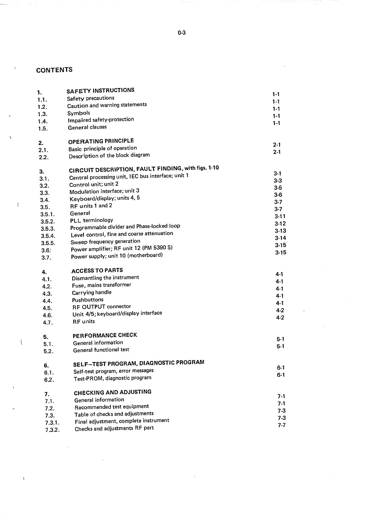
CONTENTS
1. SAFETY INSTRUCTIONS
1.1. Safety precautions
1.2. Caution and warning statements
1.3. Symbols
1.4. Impaired safety-protection
1.5. General clauses
2. OPERATING PRINCIPLE
2.1. Basic principle of operation
2.2. Description of the block diagram
3. CIRCUIT DESCRIPTION, FAULT FINDING, with figs.
3.1. Central processing unit, lEC bus interface; unit 1
3.2. Control unit; unit 2
3.3. Modulation interface; unit 3
3.4. Keyboard/display; units 4, 5
3.5. RF units 1and 2
3.5.1, General
3.5.2. PLL terminology
3.5.3. Programmable divider and Phase-locked loop
3.5.4. Level control, fine and coarse attenuation
3.5.5. Sweep frequency generation
3.6; Power amplifier; RF unit 12 (PM 5390 S)
3.7. Power supply; unit 10 (motherboard)
4. access to PARTS
4.1. Dismantling the instrument
4.2. Fuse, mains transformer
4.3. Carrying handle
4.4. Pushbuttons
4.5. RF OUTPUT connector
4.6. Unit 4/5; keyboard/display interface
4.7. RF units
5. PERFORMANCE CHECK
5.1. General information
5.2. General functional test
6. SELF-TEST PROGRAM, DIAGNOSTIC PROGRAM
6.1. Self-test program, error messages
6.2. Test-PROM, diagnostic program
7. CHECKING AND ADJUSTING
7.1. General information
7.2. Recommended test equipment
7.3. Table of checks and adjustments
7.3.1. Final adjustment, complete instrument
7.3.2. Checks and adjustments RF part
M
M
1-1
1-1
1-1
2-1
2-1
3-1
3-3
3-5
3-6
3-7
3-7
3-11
3-12
3-13
3-14
3-15
3-15
4-1
4-1
4-1
4-1
4-1
4-2
4-2
5-1
5-1
6-1
6-1
7-1
7-1
7-3
7-3
7-7

0-4
8. SAFETY INSPECTION AND TESTS AFTER REPAIR
AND MAINTENANCE IN THE PRIMARY CIRCUIT
8.1. General directives 8-1
8.2. Safety components 8-1
8.3. Checking the protective earth connection 8-1
8.4. Checking the insulation resistance 8-1
9. SPARE PARTS
9.1. General 9-1
9.2. Static sensitive components 9-1
9.3. Handling MOS devices 9-1
9.4. Soldering techniques 9-1
9.5. Parts list 9-3
10. FIGURES 30 -47
Fig. 30 Block diagram
Fig. 31 Front view
Fig. 32 Rearview
Fig. 33 Overall circuit diagram
Fig. 34 Unit 10, Unit 7; Motherboard, Power supply: componeniMay-out
Fig. 35 Unit 10, Unit 7; Motherboard, Power supply: circuit diagram
Fig. 36 Units U1 and U2: component lay -out
Fig. 37 Unit 1;CPU, lEC bus interface: circuit diagram
Fig. 38 Unit 2; Control unit: circuit diagram
Fig. 39 Unit 3; Modulation interface
Fig. 40 Unit 4; Keyboard/display interface
Fig. 41 Unit 5; Keyboard/display
Fig. 42 RFunits mounted
Fig. 43 RF unit 1:component lay-out
Fig. 44 RFunit 1:circuit diagram
Fig. 45 RFunit 2: component lay-out
Fig. 46 RF unit 2: circuit diagram
Fig. 47 RF unit 12: power amplifier
11. APPENDIX
Data sheets of Integrated circuits: HEF 4750, HEF 4751, 11C90
Principle of "Pulse swallowing"
12. CODING SYSTEM OF FAILURE REPORTING FOR QUALITY
13. ADDRESSES FOR SALES AND SERVICE

M
1.
1.1.
1.2.
1.3.
1.4.
1.5.
1.5.1.
1.5.2.
1.5.3.
1.5.4.
1.5.5.
1.5.6.
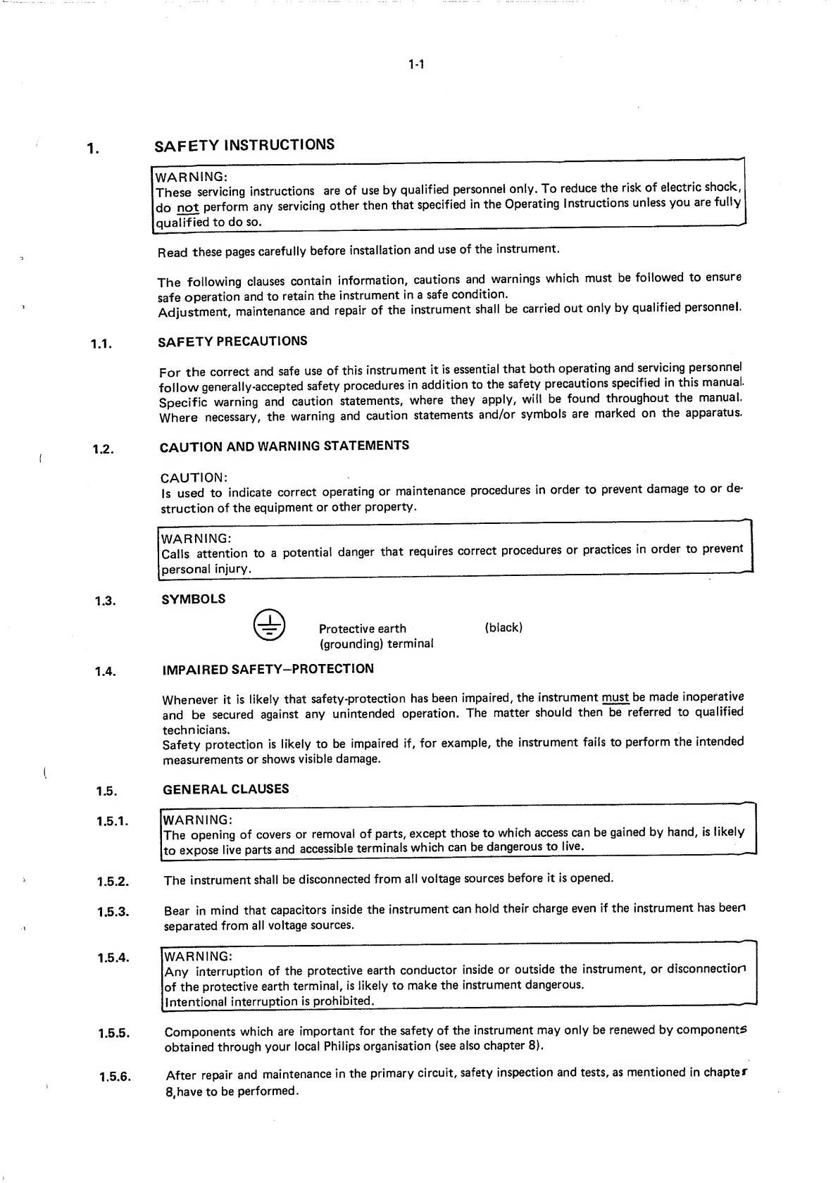
SAFETY INSTRUCTIONS
WARNING: .ui
•j*[-i0se servicing instructions are of use by qualified personnel only. To reduce the risk of electric shock,
do not perform any servicing other then that specified in the Operating Instructions unless you are fully
qualified to do so.
Read these pages carefully before installation and use of the instrument.
The following clauses contain information, cautions and warnings which must be followed to ensure
safe operation and to retain the instrument in asafe condition.
Adjustment, maintenance and repair of the instrument shall be carried out only by qualified personnel.
SAFETY PRECAUTIONS
For the correct and safe use of this instrument it is essential that both operating and servicing personnel
follow generally-accepted safety procedures in addition to the safety precautions specified in this manual*
Specific warning and caution statements, where they apply, will be found throughout the manual.
Where necessary, the warning and caution statements and/or symbols are marked on the apparatus.
CAUTION AND WARNING STATEMENTS
CAUTION:
Is used to indicate correct operating or maintenance procedures in order to prevent damage to or de-
struction of the equipment or other property.
WARNING;
Calls attention to apotential danger that requires correct procedures or practices in order to prevent
personal injury. ^
SYMBOLS
Protective earth (black)
(grounding) terminal
IMPAIRED SAFETY-PROTECTION
Whenever it is likely that safety-protection has been impaired, the instrument must be made inoperative
and be secured against any unintended operation. The matter should then be referred to qualified
technicians.
Safety protection is likely to be impaired if, for example, the instrument fails to perform the intended
measurements or shows visible damage.
GENERAL CLAUSES
WARNING;
The opening of covers or removal of parts, except those to which access can be gained by hand, is likely
to expose live parts andaccessible terminals which can be dangerous to live. ^
The instrument shall be disconnected from all voltage sources before it is opened.
Bear in mind that capacitors inside the instrument can hold their charge even if the instrument has been
separated from all voltage sources.
WARNING;
Any interruption of the protective earth conductor inside or outside the instrument, or disconnection
of the protective earth terminal. Is likely to make the instrument dangerous.
Intentional interruption is prohibited.
Components which are important for the safety of the instrument may only be renewed by components
obtained through your local Philips organisation (see also chapter 8).
After repair and maintenance in the primary circuit, safety inspection and tests, as mentioned in chapter
8, have to be performed.


2-1
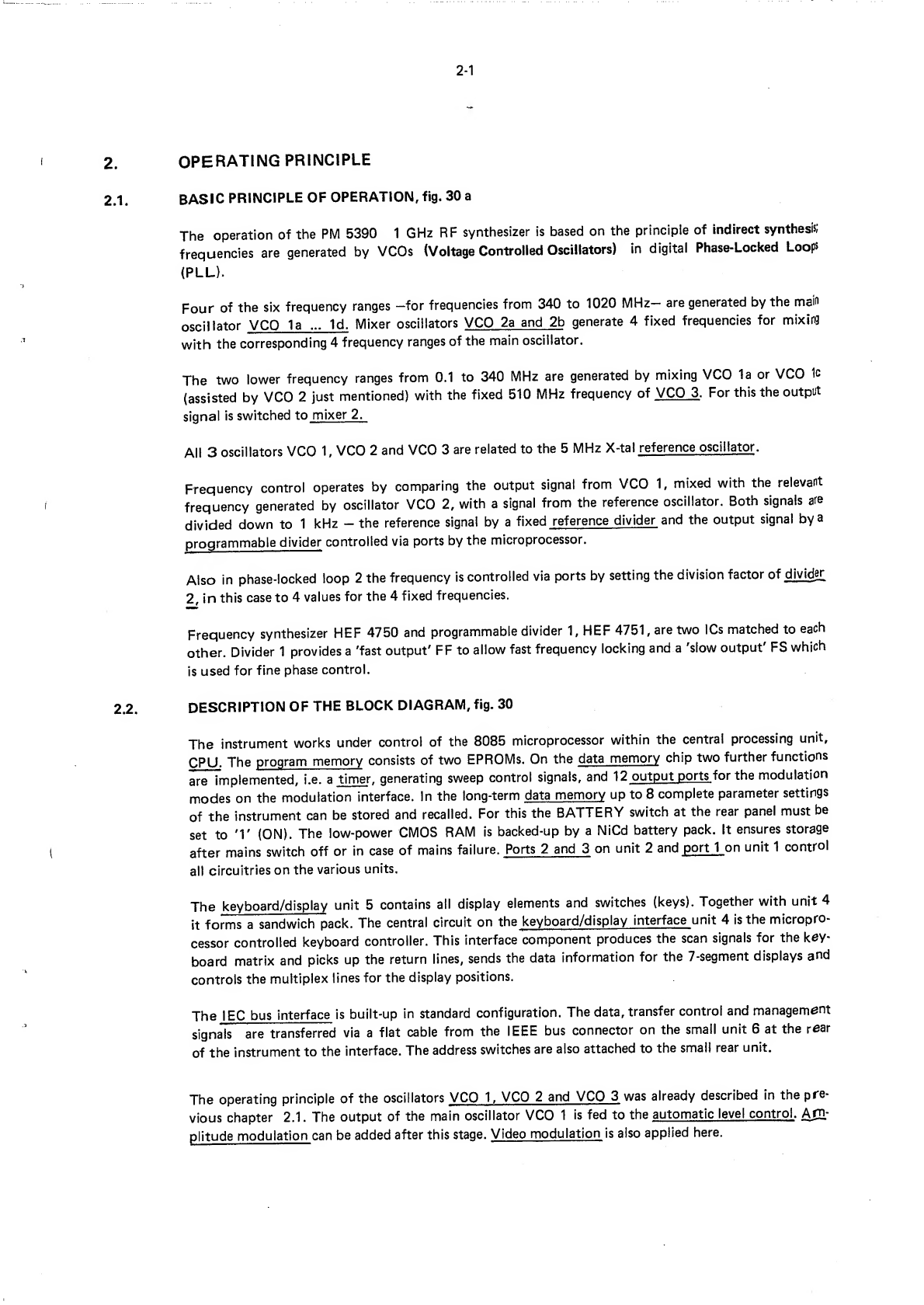
2. OPERATING PRINCIPLE
2.1. basic PRINCIPLE OF OPERATION, fig. 30 a
The operation of the PM 5390 1GHz RF synthesizer is based on the principle of indirect synthesis;
frequencies are generated by VCOs (Voltage Controlled Oscillators) in digital Phase-Locked Loops
(PLL).
Four of the six frequency ranges -for frequencies from 340 to 1020 MHz- are generated by the maid
oscillator VCO la ... Id. Mixer oscillators VCO 2a and 2b generate 4fixed frequencies for mixing
with the corresponding 4frequency ranges of the main oscillator.
The two lower frequency ranges from 0.1 to 340 MHz are generated by mixing VCO la or VCO
(assisted by VCO 2just mentioned) with the fixed 510 MHz frequency of VCO 3. For this the output
signal is switched to mixer 2.
All 3oscillators VCO 1, VCO 2and VCO 3are related to the 5MHz X-tal reference oscillator .
Frequency control operates by comparing the output signal from VCO 1, mixed with the relevant
frequency generated by oscillator VCO 2, with asignal from the reference oscillator. Both signals are
divided down to 1kHz -the reference signal by afixed reference divider and the output signal by a
programmable divider controlled via ports by the microprocessor.
Also in phase-locked loop 2the frequency is controlled via ports by setting the division factor of divider
2, in this case to 4values for the 4fixed frequencies.
Frequency synthesizer HEF 4750 and programmable divider 1, HEF 4751, are two ICs matched to each
other. Divider 1provides a'fast output' FF to allow fast frequency locking and a'slow output' FS which
is used for fine phase control.
2.2. description OF THE BLOCK DIAGRAM, fig. 30
The instrument works under control of the 8085 microprocessor within the central processing unit,
CPU. The program memory consists of two EPROMs. On the data memory chip two further functions
are implemented, i.e. atimer,generating sweep control signals, and 12 output ports for the modulation
modes on the modulation interface. In the long-term data memory up to 8complete parameter settings
of the instrument can be stored and recalled. For this the BATTERY switch at the rear panel must be
set to '1' (ON). The low-power CMOS RAM is backed-up by aNiCd battery pack. It ensures storage
after mains switch off or in case of mains failure. Ports 2and 3on unit 2and port 1on unit 1control
all circuitries on the various units.
The keyboard/display unit 5contains all display elements and switches (keys). Together with unit 4
it forms asandwich pack. The central circuit on the kevboard/display interface unit 4is the micropro-
cessor controlled keyboard controller. This interface component produces the scan signals for the key-
board matrix and picks up the return lines, sends the data information for the 7-segment displays and
controls the multiplex lines for the display positions.
The IEC bus interface is built-up in standard configuration. The data, transfer control and management
signals are transferred via aflat cable from the IEEE bus connector on the small unit 6at the rear
of the instrument to the interface. The address switches are also attached to the small rear unit.
The operating principle of the oscillators VCO 1.VCO 2and VCO 3was already described in the pre-
vious chapter 2.1. The output of the main oscillator VCO 1is fed to the automatic level control. Afn-
plitude modulation can be added after this stage. Video modulation is also applied here.
2-2
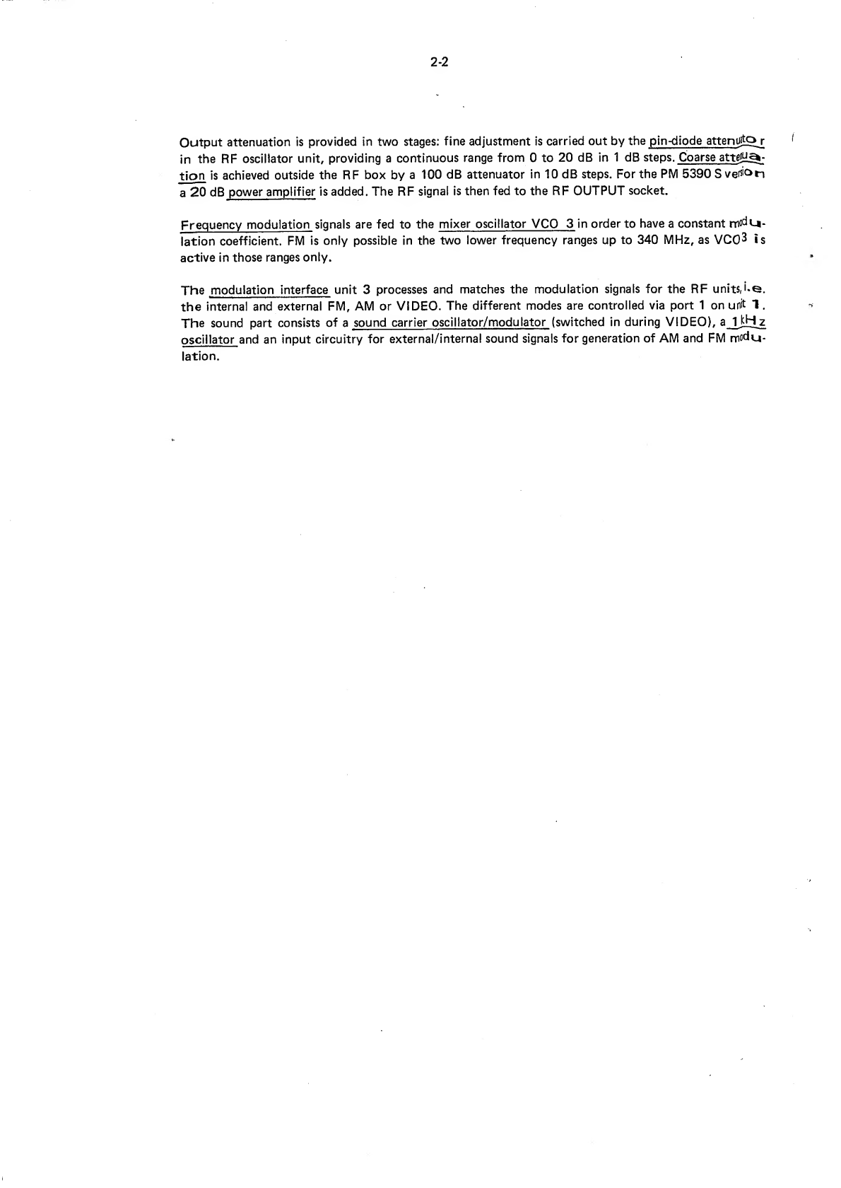
Output attenuation is provided in two stages: fine adjustment is carried out by the pin-diode atteniito r
in the RF oscillator unit, providing acontinuous range from 0to 20 dB in 1dB steps. Coarse attejH^-
tion is achieved outside the RF box by a100 dB attenuator in 10 dB steps. For the PM 5390 Svefsion
a20 dB power amplifier is added. The RF signal is then fed to the RF OUTPUT socket.
Frequency modulation signals are fed to the mixer oscillator VCO 3in order to have aconstant moclLi-
lation coefficient. FM is only possible in the two lower frequency ranges up to 340 MHz, as VCO^ is
active in those ranges only.
The modulation interface unit 3processes and matches the modulation signals for the RF units, i«e.
the Internal and external FM, AM or VIDEO. The different modes are controlled via port 1on unit 1.
The sound part consists of asound carrier oscillator/modulator (switched in during VIDEO), ajjilz
oscillator and an input circuitry for external/internal sound signals for generation of AM and FM moclu-
lation.

3-1
3.
3.1.
CIRCUIT DESCRIPTION, FAULT FINDING, PM 5390
CENTRAL PROCESSING UNIT, lEC BUS INTERFACE; UNIT 1, fig. 37
The CPU of the PM 5390 contains the 8085 microprocessor, the program and data memory and the
output ports for the modulation interface.
The 8085 microprocessor has amultiplexed address/data bus ADO-7 and the address bus A8-A15.
1C 317 latches the address information from ADO—7by means of the signal ALE (adress latch enable).
This address information at the output of 1C 317 feeds the address inputs of the program memory, ICs
306/311 and the data memory, 1C 313. The more significant address lines A8-A11, necessary for the
program memory, are directly fed from the processor to the memory chips. The address lines A12-'
A14 from the processor are decoded by the address decoder IC 320 to 'chip enable' /'chip select
signals for the memory circuits, ports and keyboard interface. The three Input lines contain abinary
information which is formed to aTout-of-8 signal at the output lines of this decoder.
The solder switches Cand Dconnect pin 21 of IC 306 either to +5 Vor to the address line A1 1to select
the PROM type 2716 or 2732 for this socket. The OR-gate 312 attaches the signals RD and 10/M to
the control signal OE {output enable) for the two PROMs. This line being 'low' enables informations
from the PROMs to be read by the processor.
Corresponding to
fied several times
In case of faulty
modifications and technical improvements during production the software was modi-
(indicated by labels on !C 306, IC 31 1/unit 1).
PROMs normally the same software has to be replaced. Please order loaded PROIvls
directly via Philips Supply Center Service, Hamburg.
The integrated circuit 318 is amultifunction chip with aRAM of 256 bytes, two 8bit and one 6bit
input/output ports and aprogrammable timer. The RAM memory is used by the processor as working
storage. Ports Aand Bsend control signals from the processor to the modulation interface, unit 3.
The third port (C) senses the states of the solder switches Eand Gwhich indicate the version of the
instrument (G for PM 5390 S) and of the lines OLOC and ODVD from the IEC bus controller 305.
The timer within IC 318 generates sweep intervals, which result from acounter value loaded by the pro-
cessor into the timer and counted down with the 30 kHz frequency of IC 302.
The timer output 318.6 sends the information 'counted down' via NOR-gate 307 to the RST 5.5 input
of the processor. When this interruption is received the processor will load the timer again with avalue
according to the required sweep interval. The resolution of the sweep time adjustment is —with the
clock frequency of 30 kHz- 1/30 000 =33.3 /is. Timer control and data handling with the processor
are performed by the control inputs CE, RD, WR, 10/M and ALE.
The integrated circuit 313 is afurther RAM memory with acapacity of 128 bytes. This CMOS RAM
stores the parameter settings; it is supplied by the built-in battery (NiCd accumulator) 805 and stores
the parameters when power is switched off. The battery can be switched off by means of switch 841
at the rear of the instrument.
Attention: The storage time is dependent on the charging state of the battery:
Storage time charging time
1day 1hour
5days 3hours
10 days 8hours
mains supply
switched off

3-2
Attention: In order to prevent damage to the battery by complete discharge, the BATTERY switch
must be set to OFF, if the instrument will not be used for approx. 3months or more.
If the battery was completely discharged by mistake it can only be loaded by desoldering
from the p.c.b. and separate loading. Damaged batteries must be replaced.
During normal operation the battery is charged from the +5 Vsupply via diode 401 and resistor 611
,
with power off diode 401 blocks the current and only the ICs 303 and 313 will be supplied by the batta-
ry. Gate 303 keeps the lines MRD and MWR in a state that no information in the circuit is destroyed
.
The low voltage detector 321 contains acomparator which switches the output pin 4to 'high' when
the supply voltage is decreased below +4.2; this switching level is determined by the resistors 614 and
616. During normal operation the low voltage detector enables the address decoder 320 and the pro-
cessor, in the moment of power off they are disables immediately.
By means of the solder switches Aand Bthe input line SID is fixed to 'low' in order to avoid distur-
bances because this input is not used.
Afurther part on unit 1is the lEC-bus interface comprising the bi-directional bus drivers 301, 304-,
308 and 314 for signal connections to the IEC bus and the IEC bus controller 305 which performs
the data transfer, handshake procedure and control functions. The switches 842 -844 at the rear of the
instrument serve for setting the IEC bus address. Shift register 315 senses the states of the switches
via the parallel inputs and gives this Information via the serial output to the serial address input, ISR
of 1C 305.
When adata transfer via the IEC bus is started, 1C 305 has to detect whether information received
address corresponds to the address set by switches 842 -844, the data transfer via buffers 309/310
is enabled by means of the signal ODVD attached with signal RD and the enable line from the address-
decoder 320. The local/remote signal from 1C 305 is sent via the buffer 309 and the NOR-gate 307
to the trap-input of the processor. Capacitor 504 and resistor 601 effect that during change from local
to remote only one short pulse is fed to the trap input; the diode 402 clips negative pulses originated
by this capacitor. The solder switch Fserves for test purposes only; the switch being open blocks the
data transfer from the IEC bus to the data bus of the processor.
The Diode 403 and capacitor 507 between the clear output OCLR, 305.33, and the Input RST 6.5
of the processor lengthens the clear pulse of the controller.
The 3MHz clock supply on unit 1 is performed with the 'elk out' signal of the processor. The clock
is divided to 1.5 MHz for the IEC bus controller and the address shift register and to 30 kHz for the
timer input. Clock division is done by the counter 302.
All general and detailed information about functions and fault finding in the lEC bus system can be
found In the 'Philips Instrumentation System Reference Manual', 9499 997 00411.

3-3
3.2. CONTROL UNIT; UNIT 2, fig. 38
Unit 2contains all ports, buffers and drivers to control the different circuits. The ports are fed with
information from the microprocessor on unit 1via the multiplexed address/data bus; this information
is stored and sent via buffers an drivers to the reed relais and attenuators by means of which the required
parameters are converted.
The ports 2and 3contain memory registers to store the data bus information from the processor and
output buffers to drive the output lines. These lines are divided into three groups A, Band C, each of
them with 8input/output lines; in this instrument they are used only as outputs.
The output lines A0-A4 of port 305 are directly fed via connector Dand buffers on the motherboard,
unit 10, to the RF unit 2for control of the programmable divider 2, ICs 308-311 .The outputs A6 and
A7 as well as B0-B3 send their information via inverting buffers 316 and connector Dto the mother-
board and control the relais 801 -806, the contacts of which switch the supply voltages for the 6VCOs
of the main oscillator in the RF unit.
The output lines B4 and B5 control the relais 808 and 807 via the transistors 337 and 338: they switch
the output signal of the pin-diode attenuator to mixer 2and actuate VC03 and the low-pass filter
U10/U1 1on the RF unit 1for the 2lower frequency ranges, 0.1 -340 MHz. All these points in the RF
unit require control voltages being quite accurate and without saturating voltage of transistors or drivers;
therefore reed contacts are used.
The transistor 335 on unit 2is not fitted in the standard version, but for the option PM 5390 S. The
input of the transistor is driven from the port output B6; the output drives arelay which activates the
20 dB power amplifier in order to get ahigher output amplitude of 1Vrms. Actuation is done by
switching the amplifier supply voltage from -12 Vto +24 V.
The remaining output lines of port 2(B7 and C0-C7) are used to control the coarse and fine attenuator
in order to set the output amplitude from -127 dBm to -7 dBm. The lines C5-C7 are converted from
TTL level at the port output to +12 V; this level is necessary to control the programmable attenuator
which sets the output level in steps of 10dBm.
Fine attenuation of the RF signal is performed by pin-diodes in the RF unit controlled by the D/A
converter on unit 2. The port outputs C0-C4 feed their currents through resistors 605 -609 into the
summing point of the operational amplifier 308. The values of these resistors are weighed. 3more lines
control the pin-diode attenuator: the outputs BO' -B2', port 3, 1C 309, are converted from TTL-level
at the port output to 12 Vlevel for CMOS; they control the solid state switches 1C 310, by means
of which the resistors 639, 652 and 653 are switched to +12 Vfeeding acurrent into the summing
point of 1C 308.
Thus with port 2, C0-C4, atotal number of 8lines control the D/A converter for the pin-diode attenu-
ator, which corresponds to aresolution of 256 points; the sum of the currents will produce avolt39s
drop at resistor 683. Thus the output of 1C 308 shows aDC-level depending on the current through
resistor 683. The working point is set by resistor/potmeter 638/681, the gain by resistor 662, depen-
ding on the characteristic of the assigned pin-diode. For further details see also chapter 3.5.4.
The programmable divider 1, 1C 301, HEF 4751, together with HEF 4750, VCO 1and two 10/1 1:1
prescaler on RF unit 2build the phase-locked loop frequency synthesizer system of the instrument,
see figs. 3and 30.

3-4
AO' -A5' of port 3, 1C 309, control the programmable divider 1. Conversion from TTL- to CMOS-
level is achieved by AND-gates 302 and 306, the outputs of which are connected via the pull-up
sistor network 601 to +10 V. These 10 Vare generated at the reference diode 401 and the resistor
604 from the 12 Vsupply. At the outputs FB2, SY, FBI the +10 Vare converted to ECL levels for th^
10/1 1:1 prescalers on RF-U2: 9.5 Vfor high, 8.2 for low level.
The frequency of the main oscillator VC01, mixed with VC02 to 50 MHz -220 MHz, is divided to
provide 2control signals for the phase comparator within 1C 314; afast 10 kHz control output FF for
fast frequency locking and aslow 1kHz control output FS for fine phase control. The division factor
50 000 -220 000 is set by 6ports AO' -A5', BCD coded, in abit-parallel, digit-serial format. The second
input of the phase comparator is the 10 kHz reference frequency, derived from the 5MHz oscillator
via the 500:1 divider within 1C 314. The program clock is 130 kHz, derived from the 5MHz oscillator
and the 23:1 divider 4, !C 307. The division factor 23:1 is achieved by connecting the outputs of 1C 30^
via NAND-gate 31 1to the reset input.
The function of the programmable divider and phase-locked loop is further described in chapter 3.5.3
with fig. 8.
Another function on unit 2is the sweep ramp generation. The sweep time divider, binary counter 312,
counts pulses sent from the timer on unit 1, input TCU. The output lines are connected to the summing
point of the operational amplifier 304 via the resistors 643 -648 the values of which are binary weighed
.
The currents through the resistors generate avoltage drop aresistor 635 in form of astaircase signal.
The output of !C 304 is connected to the SWEEP TIME OUT socket at the rear of the instrument, where
astaircase voltage from 0to 500 mV in 50 steps of 10 mV each is available; the length of astaircase
rannp, i.e. the sweep time, can be adjusted from 0.05 sto 20 s.
At each step the CPU increases the actual frequency by 1/50 of Afrequency, starting at the set FRE—
QUENCY and ending at FREQUENCY plus AFREQUENCY. Sweep is only possible within one of the
subranges.
For the sweep frequency generation and more details about the sweep ramp generation see chapter 3.5.5.

3-5
3.3. MODULATION INTERFACE, UNIT 3, fig- 39
Processing and matching of the modulation signals for the RF units, i.e. the internal and external
am or VIDEO are achieved by unit 3. The different modes are controlled via ports P1/B0-6, P1/A4-7,
P1/A0-1 of CPU, unit 1, and are switched by inverters 351/352 and FET-switches 353 ... 356. These
switches are supplied by ~2 Vat pin 7and +12 Vat pin 14.
Detailed information of the logic states and port outputs for all modulation modes is given in table fig.1
IC318 (U1) PORT1 /BO ... 6PORT1 /AO... 7
6 5 4 3 21076543210
Pin U1 B11 BIO B9 B8 B7 B6 B5 B14 B13 B12 C26 C25 C24 C23 C22
Pin U3 5678 9 10 11 234112 not used
ident. U3 E F G1KBBC D AH--
AM int 1 1 1 1 1 0 0 101 1
1
1
AM ext 1 1 011011111 1
FM int 111111011101
FM ext 111011 1 1 1 1 11
VIDEO 1 1 110111 1 1 11
VFM int 011101011010
V.FM ext 0011011 1 1 1 10
VAM int 111101001010
VAM ext 101 1 01101110,
Fig. 1Unit 1and 3; logic states of port outputs for modulation modes
The sound part consists of asound carrier oscillator/modulator (switched in during VIDEO), a1kHz
oscillator and an input circuitry for external/internal sound signals for generation of AM and FM modu-
lation.
The 1kHz oscillator is aRC oscillator based on the Wien-bridge principle, the components of which are
654, 535, 534, 659. Arectifier is added balancing the differential amplifier 307/1.2. So the stability
of oscillation and amplitude is achieved. The oscillator is switched in by 355/L.
For external FM sound signals adecoupling preamplifier 306, 307/5, 308 is available. By means of
soldering link Fthe required pre-emphasis of 50 jus can be obtained.
In VIDEO/FM-mode the modulation signal is applied via FET-switch 355/E to the sound carrier osciHa-
tor/modulator. In FM-mode (f =0.1 -<340 MHz) the FM modulation signal is applied via switches
354/H or 356/A and output FM (point 21 )directly to the RF-unit 1
.
In VIDEO/AM-mode the modulation signal is applied to the sound carrier oscillator/modulator via
FET-switch 355/B. In mode RF carrier /AM the modulation signal is fed via IC 357 to the AM am-
plifier 304/4 ... 11.

3-6
The sound carrier oscillator and -modulator is aColpitts-circuitry with transistor 309. The sound carrier
frequency can be set to 4.5 MHz, 5.5 MHz, 6.0 MHz or 6.5 MHz by means of corresponding solder links
A, B, C. For 6.5 MHz all solder links are open. Adjustment to the correct frequency is achieved by
trimmer 552, 556, 560 and 564.
The frequency modulation of the sound carrier occurs by varicap 410, whereby the deviation for 5.5
MHz is adjusted by potmeter 692. The deviation of the other sound carrier frequencies depends on tbe
capacitance ratio. Transistor 31 1serves as amplitude modulator.
The VIDEO input is ac-coupled. Async-separate circuitry (513, 614, 615, 616 and 302) separatesa
sync-clamp-pulse in order to clamp the external signal to ground by transistor 303. The external signal
is buffered by transistor 301. By scaling resistors 619 and 620 the accurate signal level is added to tte
sound carrier signal to the input of signal-addition-amplifier 304/1, 2, 3, 12, 13, 14. Positive or negative
video modulation is selected by solder links Eor D.
Adjustment of the dc-ievel at the output AM/VIDEO in video mode is achieved by potmeter 631. The
residual carrier signal is adjusted by 645.
Final amplification takes place in the second signal-addition-amplifier 304/4 ... 11 where the preampli-
fied AM-signal is applied via 547. The correct working point of this stage is adjusted without any modu-
lation by potmeter 639. During AM-mode the level of the RF carrier is reduced by 6dB, realized by
switch 353/K and resistor 633.
3.4. KEYBOARD/DISPLAY; UNIT 4. 5; figs. 40, 41
The central circuit on unit 4is the microprocessor controlled keyboard controller P8279. This interface
component produces the scan signals for the keyboard matrix and picks up the return lines, sends the
data information for the 7-segment displays and controls the multiplex lines for the display positions.
The LED sINT, AM, FM, VIDEO, EXT, REMOTE, SINGLE and CONT are driven from the port outputs
on the CPU, unit 1,via the buffers 305 and 306 on U4.
The information from the processor is fed to the keyboard controller via the data bus ADO -AD7;
^data transfer is performed by the control signals RD, WR, Clk, RES and IRQ. The chip select signal
CS is generated on the CPU-card from the address decoder 1C 320, pin 7.
Data information for the 7-segment displays is sent via the lines OUT BO -OUT B3 to the 7-segment
decoder 1C 308 which generates 7output lines for the segments, the decimal points are driven by the
outputs A1 and A2 via gate 303 or by the timer circuit 1C 307 for blinking decimal points.
The scan information is contained in the four lines SLO —SL3 which are decoded to Tout-of-16 with
the decoder 301. When the outputs of this circuit are switched on {= Low) the according display posi-
tion is lit. Thus the data information at the lines a-g (7-segment) together with the according set multi-
plex line give the complete information for each display position. Coordination of the timing between
data information and multiplex line is automatically done in the P8279.
Three of the scan lines SLO —SL2 are used to scan the keyboard matrix. The BIN -BCD decoder 304
produces the information for the scan lines of the keyboard-matrix, the return lines are connected
directly to 1C 302. Pressing one of the keys effects IRQ (interrupt request) be sent to the main processor
on Unit 1;after this it is possible to transfer the code of the key via the data lines ADO -AD7 from the
keyboard controller to the CPU card.
The integrated circuit 307 is atimer circuit which generates the flash-clock for the decimal points
(during input) or for the digits in case of exceeding the specifications for the parameters. Flashing of
the decimal points is enabled by th^puts 'FM flash' or 'VIDEO flash' being set, the blinking display
positions are effected by the output BD of 1C 302.
Unit 5contains all display elements and switches (keys) and together with unit 4forms asandwich
pack; interconnections between themselves and connections to the motherboard, unit 10, are done yia
CIS connectors.

3-7
3.5.
3.5,1.
RF UNITS 1and 2; figs, 42 -46
General
The frequency synthesis is acombination of system elements that results in the generation of many
frequencies from one or few reference sources. The frequency accuracy and stability of the device are
determined by the accuracy and stability of the crystal reference source and to aless extend the cir*
cu it.
The RF oscillator unit is the heart of this programmable frequency generator. The unit comprises the
two single screened RF units 1and 2which are mounted together with connection board RF into the
control RF box. The PM 5390 RF synthesizer is based on the principle of indirect synthesis; fre-
quencies are generated by VCOs (Voltage Controlled Oscillators) in digital Phase-Locked Loops (PL LI-
Aphase locked loop is basically an electronic servo loop consisting of aphase detector PD, alow-pass
filter and aVCO. Its controlled oscillator phase makes it capable of locking or synchronizing with an
Incoming signal. If the phase changes, which indicates that the incoming frequency is changing, the
phase detector output voltage increases or decreases just enough to keep the oscillator frequency the
same as the incoming frequency, preserving the locked condition.
INPUT
SIGNAL
ViW
A>;
Hi
OUTPUT
SIGNAL
Fig. 2Block diagram of Phase Locked Loop (PLL)
Four of the six subranges —340 to 510 MHz, 510 to 680 MHz, 680 to 850 MHz and 850 to 1020 MHz^
are generated by VCO la ... d. To get always the same dividing range Nin loop 1the output signal f1
of VCOl in this digital PLL is down converted by mixer 1to 50 MHz ... 220 MHz.
Mixer oscillators VC02 aand bgenerate 4fixed frequencies for mixing with the corresponding 4fre-
quency ranges of the main oscillator.
The resolution of the output frequency is 1kHz (10 kHz above 1000 MHz); so the divider Nmust be
set between 50 000 and 200 000 In steps of 1. This is achieved by the programmable divider 1(U2)
and two 10/11:1 prescalers (RF-U2), controlled by port 3A, unit 2.
The frequency ranges from 0.1 to 170 MHz and 170 to 340 MHz are generated by mixing VCOIa or
VCOIc (assisted by VC02 just mentioned) with the fixed 510 MHz frequency of VC03. For this the
output signal is switched to mixer 2. The lowpass filter (RF-U1/U1 1/U12) separates unwanted mix^r
products.
All 3oscillators VCOl ,VC02 and VC03 are related to the 5MHz X-tal reference oscillator.
Fig. 4shows the different oscillators involved into the frequency generation from 0.1 to 1020 MHz.

3-8
Fig. 3Principle of RF generation PM 5390
Characteristics of Indirect synthesis
Main oscillator freq. (VC01
)
fi =340 ... 1020 MHz
Conversion oscillator freq. (VC02) f2 =290/460/630/800 MHz
Converted frequency fi -f2=50... 220 MHz
Conversion oscillator freq. (VC03) fs =510 MHz
Reference oscillator frequency fosc =5MHz
Reference frequency slow loop 1fs =1kHz
Reference frequency fast loop 1fF =10 kHz
Reference frequency loop 2and 3fRef =39.0625 kHz
Divider settings:
Ref. divider for loop 1A=5000
Divider 5B=128
Progr. divider for fs N=50.000 ... 220.000
29x256 at 290 MHz
Progr. divider 2n1
{
46 X256 at 460 MHz
63x256 at 630 MHz
80x256 at 800 MHz
Ref. divider loop 3n2 =13056
The locked PLL loop 1and 2is represented by:
jN.n1 j
f1 =fosc (“X B»
e.g. frequency RF out (f1) =1000 MHz
N=200.000, A=5000, B=128; n1 =80 x256

RF subrange
Fig. 5RF unit 1and 2; table of port settings


3-11
3.5.2. Phased Locked Loop terminology (PLL)
Phase Detector (PD)
Acircuit which compares the input and VCO signals and produces an error voltage which is dependent
on their relative phase difference. This error voltage corrects the VCO frequency during tracking. Also
called Phase Comparator.
Low-Pass Filter (LPF)
Alow-pass filter in the loop which permits only dc and low frequency voltages to travel around the
loop. It controls the capture range and the noise and outband signal rejection characteristics.
Voltage Controlled Oscillator (VCO)
An oscillator whose frequency is determined by an applied control voltage.
Lock Range (2a; L)
The range of frequencies over which the loop will remain in lock. Normally the lock range is centered
at the free-running frequency unless there is some non-linearity in the system which limits the frequen-
cy deviation on one side fo. The deviations from fo are referred to as the Tracking Range or Hold-in
Range.
Free-Running Frequency (fo,coo)
Also called tne Center Frequency; this Is the frequency at which the loop VCO operates when not
locked to an input signal.
VCO Conversion Gain (Ko)
The conversion factor between VCO frequency and control voltage in radians/second/voit.
Phase Detector Gain Factor (Kd)
The conversion factor between the phase detector output voltage and the phase difference between
input and VCO signals in volts/radian. At low input signal amplitudes, the gain is also afunction of
input level.
BLOCK DIAGRAM OF PHASE LOCKED LOOP
«•
INPUT
SIGNAL
ViW
OUTPUT
SIGNAL
Table of contents
Other Philips Synthesizer manuals