manuals.online logo
Brands
  1. Home
  2. •
  3. Brands
  4. •
  5. Pioneer
  6. •
  7. CD/CDR Drive
  8. •
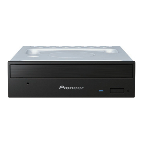
  9. Pioneer DR-2111 User manual

Pioneer DR-2111 User manual

(
@PIONEER®
The
Art
of
Entertainment
Service
Manual ORDER NO.
RRV1431
THIS
MANUAL
IS APPLICABLE TO
THE
FOLLOWING MODEL(S)
AND
TYPE(S).
Model
Type
Power
Requirement Remarks
DR-2111 DR-UP124X-5
ZUCNVL 0 0
DC
power supplied from other system component
..
CONTENTS
1.
SAFETY INFORMATION ...............
..
.
..
..........
..
..
. 2
6.
ADJUSTMENTS...
..
...............
...
.........................17
2.
EXPLODED VIEWS, PACKING AND 7. FUNCTION OF PERSONAL COMPUTER
PARTS LIST ........
...
.....................................
..
..
.
..
3 FOR SERVICING .....
..
...
.
..
..
..
...
..........................22
3.
SCHEMATIC AND PCB CONNECTION
8.
IC
INFORMATION ........
..
..............
...
.................26
DIAGRAMS ..
..
.................
...
...
..
............................?
9.
BLOCK DIAGRAM ..
...
..
..
...................................30
4.
PCB PARTS LIST ...............
..
....
.......
...
.....
..
....... 15 10. PANEL FACILITIES ..........................................
31
5.
DISASSEMBLY.
..
....
...
....................................... 16 11. SPECIFICATIONS .....................................
..
...
31
PIONEER ELECTRONIC CORPORATION 4-1, Meguro 1-Chome, Meguro-ku, Tokyo 153, Japan
PIONEER ELECTRONICS SERVICE INC. P.O. Box 1760, Long Beach,
CA
90801-1760, U.S.A.
PIONEER ELECTRONIC [EUROPE]
N.V.
Haven 1087 Keetberglaan
1,
9120 Melsele, Belgium
PIONEER ELECTRONICS ASIACENTRE
PTE.
LTD.
501
Orchard Road, #10-00 Lane Crawford Place, Singapore 0923
© PIONEER ELECTRONIC CORPORATION 1995 T-
DFR
DEC.
1995
Printed in Japan
DR-2111,
DR-UP124X-5
1.
S
AF
ET
Y INFORMATION
This service manual
is
intended for qualified service technici
an
s;
it
is
not meant for the casual
do-it-yourselfer. Qualified technicians have the necessary test equipment and tools, and have been
trained to properly and safely repair complex products such as those cove
re
d by this manual.
Improperly performed repairs can adversely affect the safety and re
li
ability of the product and may
.
void the warranty. If you are not qualified to perform the repair of this product properly and safely, you
should not risk trying to do so and refer the repair to a qualified service technician.
WARNING
Lead in
solder
used in this product is listed by the California Health and Welfare agency as a known reproductive
toxicant
which
may cause birth defects
or
other
reproductive harm (California Health & Safety Code, Section 25249.5).
When servicing
or
handling circuit boards and other components which contain lead in solder, avoid unprotected skin contact
wi
th
the solder. Also, when soldering do not inhale any smoke
or
fumes produced.
.----
(FOR EUROPEAN MODEL ONLY)
rVARO !
AVATTAESSA
JA
SUOJALUKITUS
£
OHITETTAESSA
OLET
AL
TTllNA
NAKYMA
TIC
MALLE LASERSATEILYLLE.
ALA KATSO SATEESEEN.
LASER
Kuva 1
r ADVERSEL: Lasersateilyn
USYNLIG LASERSTRALING VED ABNING varoitusmerkki
NAR
SIKKERHEDSAFBRYDERE
ER
UDE
AF
FUNKTION
UNDGA
UDSAETTELSE
FOR STRALING.
r VARNING !
OSYNLIG LASERSTRALNING NAR DENNA
DEL
AR
CPPNAD
OCH
SPARREN
AR
URKOPPLAD. BETRAKTA
EJ
STRALEN.
LABEL
CHECK
a.ASS
1
LASER
PROllJCT
LASER
KLMSE
1
CAIJTION
INVISIBl.E
LASER
RADIATDI
WHEN
Dl'EN,
AVOID
EXPOSURE
TO
BEAM
ZUC/WL model
r-
-
------
------
-.,
' '
' '
(
__
- -
---
--------
--
- l
REAR VIEW
2
.-
WARNING! £
DEVICE INCLUDES LASER DIODE WHICH
EMITS
INVISIBLE
INFRARED
RADIATION
WHICH
IS
DANGEROUS TO EYES. THERE
IS
A WARNING SIGN ACCORDING TO PICTURE
1 INSIDE THE DEVICE CLOSE TO THE LASER LASER
DIODE. Picture 1
Warning sign for
laser radiation
IMPORTANT
THIS
PIONEER
APPARATUS
CONTAINS
LASER
OF
CLASS
1.
SERVICING OPERATION
OF
THE
APPARATUS
SHOULD
BE
DONE
BY A
SPECIALLY
INSTRUTED
PERSON
.
.---
LASER
DIODE
CHARACTERISTICS -
MAXIMUM OUTPUT
POWER
: 5
mw
WAVELENGTH:
780
-
785
nm
~----
Additional
Laser
Caution
------~
1. Laser Interlock Mechanism
The position of the switch (S902) for detecting loading
completion is detected
by
the system microprocessor,
and
the
design prevents laser diode oscillation when the
switch (S902) is not in CLMP terminal side (when the
mechanism is not clamped and CLMP signal is high
level.) Thus, the interlock will
no
longer function if the
switch (S902) is deliberately set
to
CLMP
terminal side. (if
CLMP
signal
is
l
ow
level).
In
the test mode * the interlock mechanism will not
function.
Laser diode oscillation will continue, if
pin
4 of TA2066F
(IC204)
on
the
MOTHER board assy connected to GND,
or pin
19
is connected to high level (ON), or else the
terminals of
0206
are shorted to each
other
(fault
condition).
2.
When
the cover is opened, close viewing of the objective
lens with the naked
eye
will cause exposure to a
~ass
1
laser
beam
.
*Refer
to
page 18.
(
(
(
(
--
(
( .
(
(
DR-21
11,
DR-UP124X-5
2. EXPLODED VIEWS, PACKING
AND
PARTS LIST
NOTES:
•
Pa
r
ts
m
arked
by
"
NS
P"
are
ge
n
era
ll
y
unavailab
le
beca
u
se
t
hey
are
not
in
our
Master
Spare
Parts
list.
•
The
6
mark
found
on
some
component
par
ts
indicates
the
importance
of
the
safety
factor
of
the
part.
Therefore
,
when
replacing,
be
sure
to
use
parts
of
iden
t
ic
al
designa
t
io
n.
•
Parts
marked
by
"
1
~
1
"a
re
not
always
kept
in
stock.
Their
delivery
time
may
be
longer
than
usual
or
they
may
be
unavailable
.
•
Parts
l
ist
without
notice
are
common
for DR
-2111
andDR
-U
P
124X
-
5.
'
2.1 PACKING
• CONTRAST OF
DR
-2111 AND DR-UP124X-5
DR-2
111
and DR-UP124X-5 have the same cons
tr
uction except for the followin
g:
Mark
No
. Descr
ip
t
io
n
1
PadL
1 Pad(BULK)
2
PadR
NSP 3 Master carton
NSP 4 Packingcase
4 Packing case
8 Audio cable
9 Polyethylene bag
10 Screw
11
Plate
12
Install
manual
13
Programmed FD (ATAPI)
•PARTS
LIST
FOR
DR-2111
Ma
rk
No
. Descr
ip
tion
1
Pad
(BULK)
2
...
...
....
.....
..
.
3 ........-..
....
..
..
4
Packing
case
NSP
5
Poly
e
thlene
bag
6 .
..
....
...
.
....
...
7
Oper
a
ting
instructi
o
ns
(Engl
i
sh/French)
8 ..
..
...
....
...
.
..
.
9
.....
.
...
....
.....
10
..
.....
..
.
..
...
...
11
Plate
•Packing for
DR
-2111
7
5
~
o
p
~Front
Parts
No
.
DHA1353
DHG1699
Z21-
019
DR
C
10
32
DHC1045
DR
-2
111
Notused
DHA1353
Not used
Not used
Not used
DHG1699
Not used
Not used
Not used
DHC1045
Not
us
ed
Notused
Part No.
DR
-
UP1
24X-5
DHA1339
Not used
DHA1342
DHG1704
DHG1705
Notused
DKP3114
DHL1089
PMA30P050FMC
Not used
DRB1
202
DWX1669
• Packing for DR-UA124X-5
Remarks
3
DR-2111,
DR-UP124X-5
2.2 EXTERIOR SECTION
Parts List
Mark
No.
NSP
1
2
3
NSP
4
NSP
5
6
7
NSP
8
9
10
4
Description
MOTHER board assy
EP-ROM (ATAPI) (IC702)
Tray
name
plate A (ABS)
Top case
Loading mechanism A
assy
Vo
lume knob
Bottom case
Eject knob
15
...
·
...
·
··,.·
r:
.
>·
·
....
···~:.
)
,'
~
15
Parts No. Mark
DWX1666
DYW1506
DAH1775
DNC1417
DXA1787
DNK3222
DNC1395
DAC1823
6
5
Refer to 2.3 LOADING
MECHANISM SECTION.
(
No. Description Parts No.
11
Front
bezel (FOR DR-2111) DAH1803
11
Front
bezel (FQR DR-UP124X-5) DAH1802
12 65 label DRW1659
13 Screw BBZ26P080FMC
14
Short
socket DKX1039
15
Sheet
DEC1861
16 Label (For DR-2111) DRW1745
16 Label (For DR-UP124X-5) DRW1756
17 Label DRW1694
18 Screw JGZ14P040FMC
(
8
13
--
I
I(
( .
(
(
DR-2111,
DR-UP124X-5
2.3 LOADING MECHANISM SECTION
Parts List
Mark
No. Description Parts No.
1 Clamper
assy
DXA1752
2 Bridge DNE1288
3 Switch lever DNK3102
4 Lever Switch (LOADING) DSKlOOl
5 Connector
assy
3P
DKP3103
6 Drive cam DNK3097
7 Loading
gear
DNK3101
8 Belt DEB1316
9
Washer
WT21D050D050
10
Gear
pulley DNK3099
2
17
~
Mark No. Description Parts No.
11
Motor pulley PNW1634
12 Drive gear DNK3100
13 Loa'd
ba
se DNK3086
14 Motor (LOADING) DXM1077
15
Tray
DNK3087
16 Eje
ct
lever DNK3103
17 Drive lev
er
DNK3098
18 Screw IBZ26P060FMC
19 TS screw DBA1006
20 Screw
JGZl
7P030FMC
21 Servo mechanism assy DXB1580
22 PVC
sheet
DEC1875
23 Stopp
er
DNH2076
Refer to 2.4 SERVO MECHANISM SECTION.
21
19
13
NOTE :Screws adjacent
to
T mark on
the
product
are used for disassembly.
5
DR-2111,
DR
-
UP124X-5
2.4 SERVO MECHANISM SECTION
Parts List
Mark
NSP
NSP
NSP
No. Description
1
Sp
in
dle motor assy-S
2
3 T
ab
le sh
eet
4 Disc
tab
le Assy
5
6
7 Magnet
8 Sp
ind
le motor
9 Pickup assy-S
10
Gear
sprin
g
11
Fl
oat
rubber
12
Connector assy
4P
13
14
15 Mechanism base (PPE)
@--7
0
.,
4
0
0
8
Top view
Bottom view
s
Parts No.
D
XX23
11
DEC1871
DXA
1797
DNS1186
DXM1081
DXX2312
DBH1286
DEB1315
DKP3239
DNK3212
(
Mark
No
. Description Parts No.
16 Motor pinion DNK3090
17
GearA
DNK3092
18
GearB
DNK3093
19 Guide
bar
PLA1094
20 Motor
(CAR
RIAGE) DXM1077
21
Screw
JGZl
7P030FMC
22
23 Wash
er
WT26D060D025
NSP 24 TKNB UNIT DWZ1067
NSP 25 Disc
man
DNK3089
NSP 26 P.U. Assy (plastic) DWY1057
--
(
(
DR-2111,
DR-UP124X-5
3. SCHEMATIC
AND
PCB
CONNECTION DIAGRAMS
3.1
OVERALL SCHEMATIC DIAGRAM
z
0
u
a.
z
0
0
g '
<(
w
~
lL
cc
w
f-
z
f-
<i)
0
I
~
~
~
;;;
a.
"'
0
I - - ,
I
I I
I I
L-----
--
"'
00
<I)
-
Cl~
~~
o~
<Ill
Oo
-1 -
~
>-
~
~
~
~
~
.
~
s•
2g
+ + + I
u~o
o o
~~~
!=
u~
z
o
zou
w
~ z
w~
uuuu
>>
CJ_J
CJ
~>>>Cl
>
><<
<(<(
(/)
I
>-
01
(/)
<(
N
CSl
r-
0
--
-,
0.. N
~Kr-------1L
~
~
I-
"'1Z
X
~~ ~~
o:
e
L
---
-
---~~ ----
-
------------
-
--
------
~
i3
"'
..J
<
z
°'
0
0
::>
<
..
u_
"'
•
"'
<I)
f-
u
w
-,
LU
cc
0
f-
<(
u
0
z
>-
<I)
:J
"'
w
'.l
..J
a
>
~
I
a.
VJ
w
z
0
I
a.
NOTE
FOR
SCHEMATIC DIAGRAMS (Type 4A)
1. When ordering service parts, be sure
to
refer
to
•
PARTS
LIST
of
EXPLODED
VIEWSn
or
•pee
PARTS
LISTn.
'2. Since
theH
are
b11ic circuits. 1ome
puts
of
them
or
the
v1lue1
of
some
components
may
be
c
hanged
for
Improve·
ment.
3. RESISTORS:
Unit: k:
k!J,
M:MQ,
or
Q unle
ss
otherwi
se
not
ed.
Ra
ted power: 1/4W, 1/6W, 1/
fW./
, 1/
lOW
unless otherwise
noted.
Tolerance: (F): ±1%,
(G)
: ±2%, (
K)
: ±
10
%, (M): ± 20% or
±5%
un·
less
oth
erwise
noted
.
4. CAPACITORS:
Unit:
p:p
For
µF
unless otherwise noted.
Ratings: capac
ito
r
(µ.FJ
/ voltage (V) unless
otherwis
e n
ot
ed.
Rated voltage:
50V
except
fo
r electrolytic capacitors.
5. COILS:
Uni
t:
m:mH or
µH
unless othe
rw
i
se
noted.
I. VOLTAGE
AND
CURRENT:
Llor
- V :
DC voltage (V) in PLAY mode unle
ss
ot
he
rw
ise noted.
<?m
A
or-
mA
:
DC c
ur
rent in PLAY
mo
de unless othe
rwi
se noted.
Va
lue in ( ) is OC curre
nt
in
STOP
mode.
7.
OTHERS:
• @
or
0 : Adjusting point.
•
·""
: Measurement point.
• T
he
& m
ar
kfound on somecomponent pansindicates
the
im
-
pon
ance
of
the safety fac
tor
of
the parts. Therefore,
wh
en re-
placing, be su
re
to
use p
art
s of identical designation.
I.
SC
H-
0 ON THE SCHEMATIC DIAGRAM:
• S
CH
- D indi
ca
tes the dra
win
g nu
mb
er of t
he
sche
mat
ic dia-
gra
m.
(SCH stands
fo
r
sc
hematic diagram.)
9.
SWITC
HE
S (Underline indicates swi
tc
h position):
S902 LOADING
SW
MOTHER BOARD ASSY
S701 EJECT
SW
NOTE FOR PCB DIAGRAMS:
1. Part numbers in PCB dia
gram
s mat
ch
those in the schematic
diagrams.
2. Acomparison belween Iha
ma
in parts of P
CB
and schematic
dia
gr
ams is shown below.
Sym
bol in PCB
Symbol
in Sc
he
m
at
ic Part Name
Di
agrams Diagrams
B c E B c E
~
l©J©J
Transistor
B C E
B c E B c E
~
~
l©1
Transistor
B C E with resistor
D G s D G s
(0
0 O)
l@J
l@J
Field effect
transistor
D G S
Coo
o§QOQQ):l
mm
Resistor array
~
--c;?-
3- terminal
regulator
OV
ERALL SCHEMATIC DIAGRAM
_s
_c_H_-_1_1
7
DR-2111,
DR-UP124X-5
3.2 MOTHER BOARD ASSV (1/2) AND TKNB
UNIT
B
~
I
I
u
(/)
•
V1
I
>-
V1
V1
<(
£l._
::::>
"'
u
a.
0
f-
MOTHER
BOARD
ASSY(1/2)
(DWxt1
555)
TKNB
UNIT(DWZ1057)
,------------,
CN901
I
:~:E',._.-s
:~~CK]
To
SL
I
DER
MOTOR 1
,
SPOI"
s
RED
J
SPOR
·------B~=-~~~=-=:J
VF
ACTT+
ACTF+
ACTF
-
ACTT
-
VR F
+.
V
(C
4 9
1)
FHl1
VTH1033
Y+SD
l
;~~~
~
!~~!~
PO
W
ER
"""
l
!i11f--.
----<~~,__::+>,__
-..
~
"""
• 1
2V
'
""I-
--
~-
~
...
I
TRKG
ERROR AMP I
DA
SCH-2 MOTHER BOARD ASSY (1/2) AND TKNB UNIT
TRKG
FAST
COMPARATOR
I
TRKG
DRI
VE
i
2.1
'---"'===---~=:~!
C•SCH-3)
____
_____
_,,.-SL~J
(
(
-I
(
jsPJNDLE
DRIVE
j
FLOO
•
o-f-+---t+
+--1
FLOC
o-f
-+-
-+-I
C...
FLOO
·
o-f
-+-
-
~
F
L
GA.vo-f
+-
-~
(+
SC
H
-3)
SL
IDER
Kl
CK
BU
FFE
R
DR
-
2111
,
DR
-
UP124X-5
..
,
RF
&
AUDIO
SIGNAL
ROUTE
SCH-2
~------+----------------------~,'A~=~~;
~------'----------------------~~~~
A
BUS1
~-
---
-1---
------
-------------~~
-A suse
~---
-J.--
---------
-----------~-A~A~~I<
v+so
"*'·
HEAO PHONE
.JACK
JA60
1
Dl<N1123
SCH-2
MOTH
ER
BOARD ASSY (1/2) AND TKNB UNIT 9
DR-2111,
DR-UP124X-5
3.3 MOTHER BOARD ASSV (2/2)
10
1
V+
SD
LC321'-'-4
BU
SY
LED
V+SA""
~
~
b~
7
~
~d
GR
E
EN
~tt,A-
--
-~
BUSY
~Q701
~OTC12'1-EV
V
+SA
~f
0--
-----
ft-
E
JE
CT
E
JECT
SW
~1-nD
~.
~g~g~NG
[•M+!
BL
ACKJ
0--~
0
c
'-"
.
~"-
4
~
~--~
~:]
(+
SCH
-2
)
(
..
SC
H- 1 ) E
M-(R
ED
) 0
..
,....
LOADING
SW
(+
SC
H-
1)
V+
S:
]~
9 0
i
~
~
~
G
A
&~
PC
[ 1
;;::i_
S
EL
ECT
ION
's
•. 1,u
JUM
PER
i
u-•
SCH-3
V+
'5D V
+5
D
_ft
LPS2
( +
SC
H- 2 ) -
MOTHER BOARD ASSY (2/2)
MOTHER
BOARD
ASSY
(2/ 2)
(DWX
1555)
[
~~~~~
SOA
T
A{~)
~
{CSP)
LRC~
~A~-
------
( +
SC
H-2)
(DSPJ
c2PO
,;::i;::::::_:::_:::_:::_-::_-::_-::__-~
IOSPl
l.1C
K
..
~
c~r
=
TB~
di,0
~
~
CSAC
4 . Oa.4GCM
......
V+
SO
V+SO
( (
V+SO
~f
GN
OO
RD
-.._
_.:_
__
_
-llii-"l'I>
a.f!o
! C 7 0 2
aflbo
DYW
1
505
EX
TE
R
NA
L Ro.1 H L
MA
SK,
SOCKET H H L
( 0 1 2
DR-2111,
DR-UP124X-5
V+SO
(R7
'lH
-
..,o
(R7'92~~
(R7
'33
0
(R
7'34 0
(R795
~
0
:.
1'1
.
v+
so
LE
DEVICE
CO
N F
IGURA
TI
O
N
~
JU
M
PER
V+
SD
~~
~
<t
~
i
~
~
~lt
j CN
75
1
r+
-
------
----
----
----
--+-<
>--
-
~
~~~~-1
02(l):·:
·
·
~
s •
I)
<lN~
O
I
SCH
- 3
HR
ES
ET
ON
DO
HD
67
HO
SS
HDB G
HDB'3
HD
B5
MOTHER BOARD ASSY (2/2)
...
I
_s_c_H
__
-_
3
_
w
u
<{
LL
"'
LU
1-
z
1-
(/)
0
:r:
1 1
DR-2111,
DR-UP124X-5
12
The parts mounted on this PCB include all necessary parts
for several destinations.
For further information for respective destinations, be sure
to check wtth the schematic diagram.
;;;<1JP
CBll!ll=.,.?:-
t-
t..
·n,611!.!l>l;t.111:'1ltt1'ilt!IE1':1v1:!L'ltT.
M!:1'illil'1l!fWl;t.
liilMlli:!lllBTi>.l:?l=t..i:<t::~L'.
•This
diagram is viewed from the pink col-
ored
fo
il
side.
•This
is
a multi-layer PCB.
But information for both sides is shown.
·•n~z•
~~
~-~-~SI~~Z9
.
·~~&•~-~&•z9
.
•~~2~i
:t~:T-;~T~IJ:t9
.
DNP1728-r:.1
VA651
Q603
Q602
IC702
IC853
IC703
IC707
IC709
IC70B
IC711
IC861
IC770
IC601
IC301
IC204
Q206
IC202
IC203
IC410
IC401
Q619
Q620
IC551
IC405
IC602
Q701
(
--
I
I • This diagram is viewed from the gray col-
ored foil side.
• This is a multi-layer PCB.
But information for both sides is shown.
DR-2111,
DR-UP124X-5
·
~
~
~
-
~~
~~~
~S
I
~~~
9
.
-
~~
&
•~~
~&•
~
~
.
-
~
~2
~
f
R~~
~T
~f
J
*9
•
1 3
DR-2111,
DR-UP124X-5
Waveforms of MOTHER BOARD Assy
X1 RF 0.5v/div, 0.5µs/div
X4 RF 0.5v/div, 0.1µF/div
(g)CH1
@CH2
FOCUS IN
CH1
:
FE
0.5v/div, 100ms/div
CH2 : IC2
04
-pin13 (SBAD) 1.0/div, 100ms/div
1 4
FOCUS IN
FE
0.5v/div, 2ms/div
- GND
X4 MULTl TRACK JUMP (FWD)
TE
0.5v/div, 1ms/div
-GND
X4 MULTl TRACK JUMP (REV)
TE 0.5v/div, 1ms/div
@cH1
@CH2
CH1
, 2
~"°"'"""'""""""""""'~~"""'~
·
-GND
X4 SEARCH (FWD FULL STROKE)
CH1
: TE 0.5v/div, 50ms/div
CH2 : IC4
01
-PIN18 (SLOUT)
2.0v/div, 50ms/dlv
@CH1
@CH2
CH1
, 2
-GND
X4 SEARCH (REV FULL STROKE)
CH1
:
TE
0.5v/div, 50ms/div
CH2:
IC401
·PIN18 (SLOUT)
2.0v/dlv, 50ms/dlv
X1 PLAY
CH1
: TE 0.5v/div, 100ms/div
@cH1
@CH2
CH1
, 2
-GND
CH2 :
IC50HN
1.0v/div, 100ms/div
@cH1
@CH2
-GND
X4 SEARCH
(FWD
FULL STROKE)
CH1
: TE 0.5v/di
v,
500ms
CH2 : IC5
0HN
1.0v/div, 500ms/div
@
CH1
@CH2
-GND
X4 SEARCH (REV FULL STROKE)
CH1
:
TE
0.5v/div, 500ms/div
CH2 :
IC501
-
IN
1.0v/div, 500ms/div
X4 PLAY
CH1
:
TE
0.5v/div, 20ms/div
@
CH1
@CH2
-GND
CH2 : IC501-IN 1.0v/div, 20ms/
di
v
@CH1
@CH2
-GND
X1 SEARCH (FWD FULL STROK
E)
CH1
:
TE
0.5v/div, 500ms/div
CH2 :
IC501
·IN 1.0v/div, 500ms/div
@
CH1
@
cH2
+-GND
X1 SEARCH (REV FULL STROK
E)
CH1
:
TE
0.5v/div, 500ms/div
CH2 : IC501-IN 1.0v/div, 500ms/div
X4 STILL
TE 0.5v/div, 500µs/div
(
\
(
(
(
--
-
I
I
DR-2111,
DR-UP124X-5
4. PCB PARTS LIST
NOTES:
• Parts markedby
"NSP"
are generally unavailable because they are
not
in
our
MasterSpare Parts List.
• The 6 markfound
on
some componentparts indicates the importance
of
the safetyfactor
of
the part. Therefore, when replacing,
be sure to use parts
of
identicaldesignation.
• Parts markedby " ie) " are notalways kept in stock. Their delivery time may be longer than usual
or
they may
be
unavailable.
• When ordering resistors, first convert resistance values into codeform as shown in thefollowing examples.
Ex
. 1 When there are 2 effective digits (any digitapartfrom 0), such as560 ohm
and
47kohm (tolerance is shown
by
J = 5%,
andK=
10
%).
560{2-56x10
1 = 561 ............
......
...........
.......
RDJ/4PUffi][]JITJJ
47kD
-47xl0
3
=473
..................
....
..............
RDJ/4PU@J[l]
[l]J
0.5
{2
-
ORS
...........
..
......................................
RN2H
lliJ
ffiJ ffiJ
K
JD
-IRO
.....................................
...
..............
RSJP
[I]ffi]lli] K
Ex. 2 When there are 3 effective digits (such as
in
high precision metalfilm resistors).
s.62k
n -
s62
x 101 =s621 ..............................
RM
114pc
rn
[]]
rn
rn
F
Mark
No. Description
LIST OF
PCB
ASSEMBLIES
MAINBASSY
NSP
I-
MOTHER BOARD ASSY
NSP
LTI<NB
UNIT
MOTHER BOARD ASSV
SEMICONDUCTORS
IC203
IC551
IC401
IC410
IC861
IC853
IC602
IC711
IC770
IC204
IC707
IC708, IC709
IC703
IC301
IC405, IC601
IC202
Q206
Q602, Q603, Q619, Q620
Q601
Q701
D702
COILS
AND
FILTERS
L603-L605
FlOl
(lOOOOP)
SWITCHES
AND
RELAYS
8701
CAPACITORS
C302
C427
C861
C314, C315
C601, C604
Parts No.
DWM1538
DWX1666
DWZ1067
BA10393F
BA6195FP
BA6797FP
BU4053BCF
LC321664AJ-80
LC895194-X07
M5218AFP
MB90T673
S-80742AN-D6
TA2066F
TC74HC138AF
TC74HC573AF
TC7S04F
TC9406F
XRA4558F-P
XRA4560F
2SB1189
2SC4081
DTA124EU
DTC124EU
SLB-25MGTB7
PTL1014
VTH1033
DSG1057
CCSRCH101J50
CCSRCH151J50
CCSRCH181J50
CCSRCH200J50
CCSRCH330J50
Mark No. Description
C222,C228,C428,C713,C714
C244, C855-C857
C602,C603,C605,C606
C607, C608
C510,C609,C610,C617
C404
C231, C407
C107
C858
Cl05
C201, C245, C247
C430
C227,C230,C304-C307
C711, C712
C309, C310
C512
C414, C415
C101,C112,C202,C233,C238
C242,C243,C246,C301,C303
C308,C312,C313,C321-C323
C390
,C403,C419,C423,C425
C504,C511,C611,C612
C615,C616
,C
618,C701-C704
C715,C718,C770-C773
C831,C832,C851-C853
C862, C863
C405,C417,C418,C426,C710
RESISTORS
VR651 (100)
VR201 (2.2k0)
R2
53(220)
R403 (l.OQ)
Other Resistors
OTHERS
CN601 CONNECTOR
CN201 FLEXIBLE CONNECTOR
CN751, CN752 PIN HEADER (6P)
CN151 ATAPl/POWER SUPPLY
CONNECTOR
CN401 KR CONNECTOR
Parts No.
CCSRCH390J50
CCSRCH470J50
CCSRCH820J50
CEAL100M6R3
CEAL101M6R3
CEAL470M16
CEAL470M6R3
CEAS101M16
CEAS101M6R3
CEAS221M6R3
CKSQYF105Zl6
CKSRYB102K50
CKSRYB103K50
CKSRYB103K50
CKSRYB153K50
CKSRYB223K25
CKSRYB333K16
CKSRYF104
Z25
CKSRYF104Z25
CKSRYF104Z25
CKSRYF104Z25
CKSRYF104Z25
CKSRYF104Z25
CKSRYF104Z25
CKSRYF104Z25
CKSRYF104Z25
CKSRYF473Z25
DCS1037
PCP1025
DCN1050
DCN1051
RS1/16SoooJ
103672-3A
52207-1690
9022B-06A
9047B-43Z01
B4B-PH
-
K-S
1 5
..
DR-2111,
DA-UP124X-5
Mark
No.
Description
Parts No.
X701 CERAMIC RESONATOR CSAC4.00MGCM
(4MHz)
x IC SOCKET (40P) DKH1016
JA601
MINI
JACK
DKN1123
X301 (33.8688MHz) DSS1076
CN703 CONNECTOR (3P) S3B-ZR-SM3A
TKNB UNIT
OTHERS
CN901 KR CONNECTOR S4B-PH-K-S
5.
DISASSEMBLY
• DISASSEMBLY THE FRONT BEZEL ASSY
•
Open
the
Tray
1.
Make
the
key by using clip etc.
(It
may
use to
the
metal
sick which is
extent
of
1
mm
in
diameter
and
50
mm
long.)
2. Open
the
door
by
moving
the
eject leverwhich is inserted
the
key to
the
hole
in
vertically
and
pressing
it
as shown
in
Fig. 5-1.
3. Unhook
the
two hooks of
the
tray
name
plate.
•
Remove
the
Bottom
Case
1.
Remove
the
four screws
CD
to remove
the
bottom case.
•
Remove
the
Top
Case
1.
Be careful
of
the
hooks (right
and
left)
of
the
front bezel
assy.
16
Eject
lever
it Upper side
Clip
Front
bezel
assy
Fig.5-1 Disassembly (Bottom view)
(
(
(
(
-
DR-2111,
DR-UP124X-5
6.
ADJUSTMENTS
6.1
FUNCTION
TABLE
OF
THE
REMOTE
CONTROLLER
(RU-V101)
FOR
SERVICE
•Test
Mode
Shows
the
function table
of
th
e remote controller (RU-VlOl) for service as follows. Whenoperating
the
CD-ROM directly,
it
is
possible to operate
as
shown below byconnecting
the
wired-remote control'
to
the
CD-ROM
with
the
interface.
When
the
test
commandis used,
put
in
the
shortsocketto
MA,
SL
and
GND pins
of
pinheader
(C
N751)
on
the
re
ar
panel,
and
turn
the
power on. (Refer
to
Fig.
2).
• Schematic Diagram of
the
Conversion Jig for Remote Control Operation
Interface
r--------------------
------1
•3P mini
jock
I
I
I
1PH
type
connector
(4P)
I
I
I
01
:
DTC124ES
or
UN42121
~------------------
-
------
-
J
2 1 0
Al.00
OOT
R G G l
Fig.1
39
40
ATAP
I
OODODDOD
DD
ODDDOO
DDOO
ODDDDOOOOO
DDDDDD
DDD
Put in the short socket
Fig.2
DC
INPUT
+5 G G +12
0000
1 7
DR-2111,
DR-UP124X-5
(
REJECT : Spindle stop
REJECT
..
PAUSE
II
PLAY~
PAUSE : Pause
= = PLAY ; : Play
~II
STILL/STEP
II~
STILUSTEP
II~
JTest command
-MUL
Tl-SPEED+
STILUSTEP ...II
.,_SCAN~
MULTI-SPEED+ JTest command
MULTI-SPEED -
SCAN
~
: Scan FWD
= = SCAN
........
: Scan REV
CLEAR FUNC
7 8 9 CLEAR : Clear
= = = FRAME :
Frame
set
AUDIO SPEED
OPEN
4 5 6 TIME : Time
set
= = = CHAPTER : Track
set
VIDEO STOP.M START
1 2 3 SEARCH : Search
= = =
DISPLAY STILL
C-MODE
lOkey
: Numerical
input
0 SEARCH .DISPLAY (FUNC +
1)
:No
entry
=
CR
STILL (FUNC +
2)
:No
entry
FRAME TIME CHAPTER C-MODE (FUNC +
3)
:No
entry
= = =
A 8 c VIDEO (FUNC +
4)
:No
entry
STOP.M
(FUNC +
5)
: Stop
marker
RU-V1P1 START (FUNC +
6)
:
Start
AUDIO (FUNC +
7)
:No
entry
SPEED (FUNC +
8)
:No
entry
OPEN (FUNC +
9)
: Door open (
•Test
Command
Key Operation Command Description
[OJ+
[TIME]
{OTM}
All servo OFF
[1]
+[TIME]
{lTM}
Laser-diode
(LD)
ON (
[2]
+[TIME]
{2TM}
Focus ON
[3]
+[TIME]
{3TM}
Spindle ON
[4]
+[TIME]
{4TM}
Spindle!I'racking ON/OFF
[5]
+[TIME]
{5TM}
Slider circumferential feed
[8]
+[TIME]
{8TM}
Spindle rotation frequency :Normal speed
[9]
+[TIME]
{9TM}
Spindle rotation frequency :fourfold speed
[STILUSTEP
»]
{SF}
1
Tra
c
kjump
: FWD
[STILUSTEP
«]
{SR}
1
Trackjump:
REV
[*]
+
[*]+[*]+[MULTI-SPEED+]
{*
**MF}
***Track
jump:
FWD
[*]
+ [*] +
[*]
+ [MULTI-SPEED-]
{***MR}
***Track
jump:
REV
18
(
DR-2111,
DR-UP124X-5
6.2 ADJUSTMENT METHODS
If
a disc playeris adjusted incorrectly orinadequately,
it
may malfunction or notwork
at
all even though there is nothing
at
all wrong with
the
pickup or
the
circuitry. Adjust correctly following
the
adjustment procedure.
• Adustment Items/Verification Items and Order
If
the
specified values cannot be obtained or no adjustment is possible by performing
the
verifications
or
adjustments
described in steps 1-3,
the
pickup block may be defective.
Step Item Test Point
1 Focus offset verification FO,
ERR(FE
)
2 Tracking
error
balance verification
TR,ERR(TE
)
3
RF
level
adjustment
(RF level) RF
Note : The digital servo
IC
(TC9406F) being
us
ed
in
this
set
has
the following functions
and
does
not
provide focus offset,
focus
servo
loop
gain
and
tracking
servo
l:oop
gain
adju
stments.
1. Average Function
For
accurate
servo
control,
FO
.
ERR
and
RF
average
measurements
are
performed
and
the
measured values
are
compensated through a compensation circuit.
Thus, volume control for Foucus offset
adjustment
is
not
provided.
2. Auto Gain Control Function
The gaininside
the
filter is automatically adjusted
to
obtain a
propergainintheservo
loop.
Thisfunction permitstheoptimum
gain to be obtained on each disc.
Thus,volumecontrolsfor FO.
GAIN
and
TR
.
GAIN
adjustments
are
not provided.
The gain adjustment is done before
TOC
reading.
•Measuring
Instruments and Tools
1.
Dual trace oscilloscope (10 : 1probe)
2.
Test disc (YEDS-
7)
3.
Standard
tools
Adjustment Location
None
None
VR201
•Abbreviation Table
FO. ERR(FE)
TR.
ERR(TE)
FOGAN
TRGAN
: Focus
Error
:Tracking
Error
: Focus Gain
:Tracking Gain
19
---
DR-2111,
DR-UP124X-5
G
(D(D
G
©0
©©
Fig. 3 Adjustment Locations
1. Focus Offset Verification
•Objective
• Symptom when out
of adjustment
• Measurement
instrument
connections
[Procedure]
Verify
the
DC
offset for
the
focus error amp.
The model does not focus
in
and
the
RF signal is dirty.
Connect
the
oscilloscope to • Player state
VREF(CHl),FO
.
ERR
(CH2).Refer
to
Fig.
3.
• Adjustment location
[Settings] 1V/divsion.
lOms/divsion.
DC
mode
•Disc
Focus
and
spindle servos closed
None
YEDS-7
1.
Perform
the
automatic adjustment (offset, balance and gain)
at
the
playeris playbacked by pressing
the
PLAY key.
2.
Close
the
focus servo.
3.
Verify
the
focus errorvoltage
at
the closed is
the
same voltage
(A
=
B)
as
the
VREF voltage.
CH1•
........
, •.
•••
-.r-.1.•.
.r•1
..
1
..
_11~n~~~.-
. . .
VREF
lA
-GND_L_
A=B
CH211
wr
lit#'
•ae
ttua•
PAI
. --
GND!
Not
e :
If
the specified
valu
es cannot be obtained
or
no
adjustm
e
nt
is possible by performing the verifications
or
adju
s
tm
e
nts
described
in
adjustment
items 1
-3,
thepickup block
may
be
defective.
2 0
(
(
--
I
DR-2111,
DR-UP124X-5
2. Tracking Error Balance Verification
•Objective
• Symptom when out
of adjustment
To
verify
that
there
is no variation
in
the
sensitivity
of
the
tracking photo diode.
Play does
not
start
or
track
search is impossible.
• Measurement
instrument
connections
Connect
the
oscilloscope to
TRK
• Player state
ERR. (This connection
may
be
via a low
pa
ss filter.)
Test
mode, focus
and
spindle
servos closed
and
trackingservo
open
[Settings]
[Procedure]
50 mV/division.
5 mSec/division.
DC
mode
• Adjustment location None
•Disc
YEDS-7
1. Move
the
pickup
to
midway across
the
disc (RJ\A35 mm) with
the
SCAN FWD
C>I>
or
REV <l<J key.
2.
Press
the
[1]
+ [TIME] key,
the
[2]
+ [TIME] key,
th
en
the
[3]
+ [TIME] key
in
that
orderto close
the
focus servo
then
the
spindle servo.
3.
Line
up
the
brightline (ground)
at
the
verybottom grid line of
the
oscilloscope screen
and
put
the
oscilloscope into
DC
mode.
4. Supposing
that
the
positive amplitude of
the
tracking
error
signal
at
TR. ERR is
(A)
and
the
negative amplitude
is
(B),
the
following expression is satisfied.
TI
A;tB
When
A~8
,
A-8
X1.
~0
.
5
c 2
When
A<
8,
8-A
X
..!_
~0.5
c 2
3.
RF
Level Adjustment
c 1
ii
II\
When there is a
DC
component
•Objective
To
optimize
the
playback RF signal amplitude.
• Symptom when out
of adjustment No play
or
no search
TR REF
• Measurement
instrument
connections
Connect
the
oscilloscopeto
TRK
• Player state
ERR. (This connection
may
be
via a low pass filter.)
[Settings] 50 mVIdivision. • Adjustment location
lOmSec/division.
DC
mode • Disc
[Proced
ur
e]
T A=B
1
J TR REF
If\
l
When there is no DC
component
T
est
mode, play
VR201 (Laser power)
YEDS-7
1.
Move
the
pickup to midway across
the
disc (R=35 mm)
with
the
SCAN FWDI or REV !key,
then
press
the
[1]
+ [TIME] key,
the
[2] + [TIME] key,
th
e
[3]
+ [TIME] key,
then
the
[4] + [TIME] key
in
that
order
to
close
th
e
respective servos
an
d
put
th
e player into playmode.
2. Line
up
the
brightline (GND)
at
the
verybottomgridlineof
the
ocilloscope screenand
put
the
oscilloscop
~
into
DC
mode.
3. Adjust VR201 (Laser Power)
so
that
the
RF
signal amplitude is 1.8
Vp--p±O
.l
V.
(Refer
tothe
waveforms
of
MOTHER
BOARDAssy)
2 1

This manual suits for next models

1

Other Pioneer CD/CDR Drive manuals

Pioneer BDR-XD08TB User manual

Pioneer

Pioneer BDR-XD08TB User manual

Pioneer BDR-XS07CS User manual

Pioneer

Pioneer BDR-XS07CS User manual

Pioneer BDR-XD08B User manual

Pioneer

Pioneer BDR-XD08B User manual

Pioneer BDR-S08XLT User manual

Pioneer

Pioneer BDR-S08XLT User manual

Pioneer DVR-112 User manual

Pioneer

Pioneer DVR-112 User manual

Pioneer BDR-208EBK User manual

Pioneer

Pioneer BDR-208EBK User manual

Pioneer DR-504S User manual

Pioneer

Pioneer DR-504S User manual

Pioneer DVR-104 User manual

Pioneer

Pioneer DVR-104 User manual

Pioneer BDR-XS07TS User manual

Pioneer

Pioneer BDR-XS07TS User manual

Pioneer DR-506S User manual

Pioneer

Pioneer DR-506S User manual

Pioneer DR-706S User manual

Pioneer

Pioneer DR-706S User manual

Pioneer DR-UA124X-2 User manual

Pioneer

Pioneer DR-UA124X-2 User manual

Pioneer DW-S114X User manual

Pioneer

Pioneer DW-S114X User manual

Pioneer BDR-2207 User manual

Pioneer

Pioneer BDR-2207 User manual

Pioneer DVR-S201 User manual

Pioneer

Pioneer DVR-S201 User manual

Pioneer BDR-X13E-S User manual

Pioneer

Pioneer BDR-X13E-S User manual

Pioneer BDR-2213 User manual

Pioneer

Pioneer BDR-2213 User manual

Pioneer DRM-UF701 User manual

Pioneer

Pioneer DRM-UF701 User manual

Pioneer DVR-SK12D User manual

Pioneer

Pioneer DVR-SK12D User manual

Pioneer BDR-XD05S User manual

Pioneer

Pioneer BDR-XD05S User manual

Pioneer DVR-109 User manual

Pioneer

Pioneer DVR-109 User manual

Pioneer BDR-S13U-X User manual

Pioneer

Pioneer BDR-S13U-X User manual

Pioneer DRM-600 User manual

Pioneer

Pioneer DRM-600 User manual

Pioneer DVR-A09XLC User manual

Pioneer

Pioneer DVR-A09XLC User manual

Popular CD/CDR Drive manuals by other brands

Yamaha CD Recordable/Rewritable Drive CRW2200 owner's manual

Yamaha

Yamaha CD Recordable/Rewritable Drive CRW2200 owner's manual

Samsung SH-C522C user manual

Samsung

Samsung SH-C522C user manual

Kenwood TrueX Series Quick install guide

Kenwood

Kenwood TrueX Series Quick install guide

Sony DRU-530A Product information

Sony

Sony DRU-530A Product information

HP CD-WRITER Plus user guide

HP

HP CD-WRITER Plus user guide

Panasonic LF-1007AD operating instructions

Panasonic

Panasonic LF-1007AD operating instructions

Sony PCG-GRT Series Replacement instructions

Sony

Sony PCG-GRT Series Replacement instructions

Lenovo 41N5631 user guide

Lenovo

Lenovo 41N5631 user guide

Samsung SW-248F user manual

Samsung

Samsung SW-248F user manual

Plextor 12-20D manual

Plextor

Plextor 12-20D manual

Amacom Technologies Baby CDRW user manual

Amacom Technologies

Amacom Technologies Baby CDRW user manual

LG DRD-8120B owner's manual

LG

LG DRD-8120B owner's manual

Asus Dual-Interface External Slim Combo Drive... user manual

Asus

Asus Dual-Interface External Slim Combo Drive... user manual

Panasonic CF-VDRRT2 operating instructions

Panasonic

Panasonic CF-VDRRT2 operating instructions

Sony CRX175M user guide

Sony

Sony CRX175M user guide

Aiwa BZG-2 Service manual

Aiwa

Aiwa BZG-2 Service manual

HP CD-WRITER Plus user guide

HP

HP CD-WRITER Plus user guide

Plextor 4PS-3 Operation manual

Plextor

Plextor 4PS-3 Operation manual

manuals.online logo
manuals.online logoBrands
  • About & Mission
  • Contact us
  • Privacy Policy
  • Terms and Conditions

Copyright 2025 Manuals.Online. All Rights Reserved.