Portwell NAR-5620-0100 User manual

NAR-5620 Series
Communication Appliance
Users Manual
Revision: 0.0
CE
This certificate of conformity of NAR-5620 series with actual required safety standards in
accordance with 89/366 ECC-EMC Directive and LVD 73/23 ECC
UL
This product meets all safety requirements per UL60950 standard.
Portwell Inc.
3F, No. 92, Sec. 1, Nei-Hu Rd., Taipei 114, Taiwan, R.O.C.
Headquarter: +886-2-2799-2020 FAX: +886-2-2799-1010
http://www.portwell.com.tw
Email: info@mail.portwell.com.tw

NAR-5620 Series User’s Manual 1
Table of Contents
Chapter 1 Introduction...........................................................................................................2
1.1 About This Manual ..........................................................................................................2
1.2 Manual Organization.......................................................................................................2
1.3 Technical Support Information.........................................................................................2
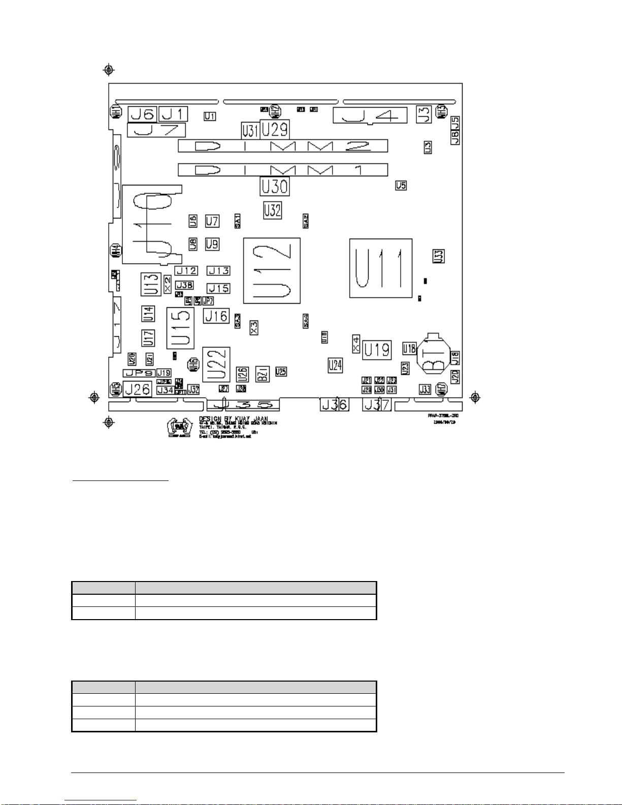
1.4 Board Layout...................................................................................................................3
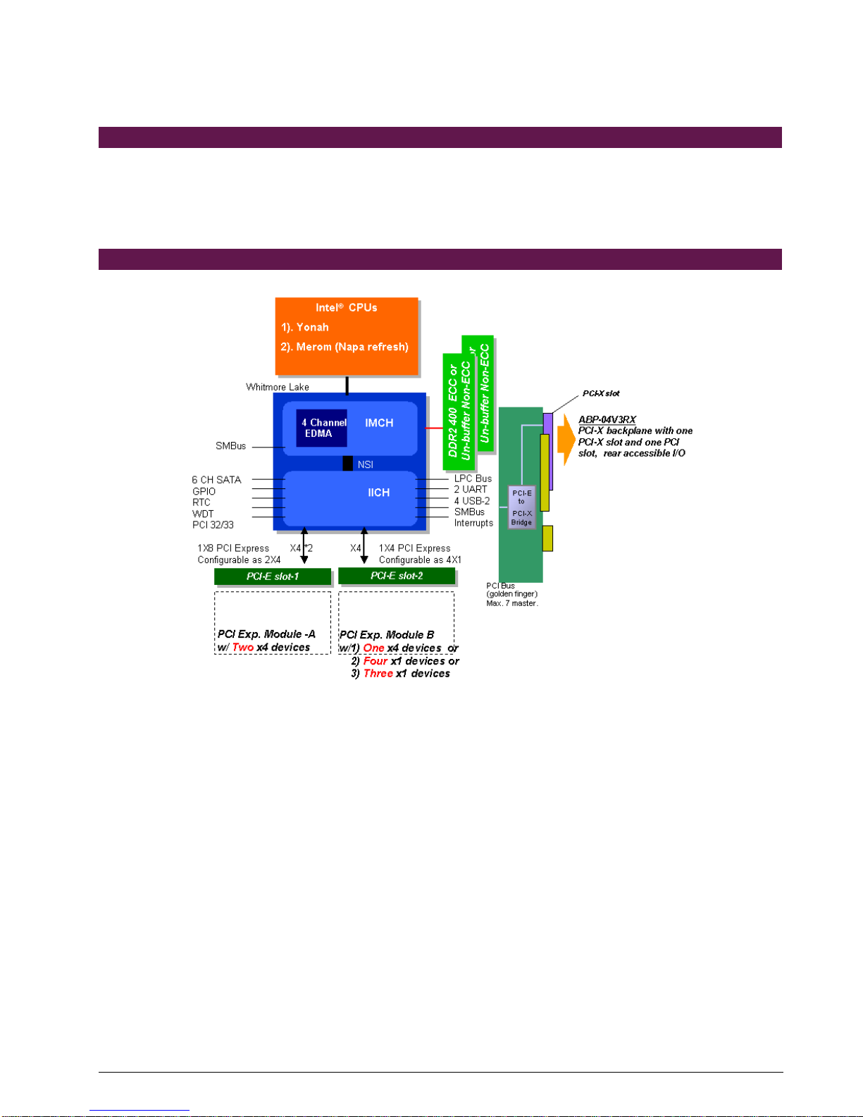
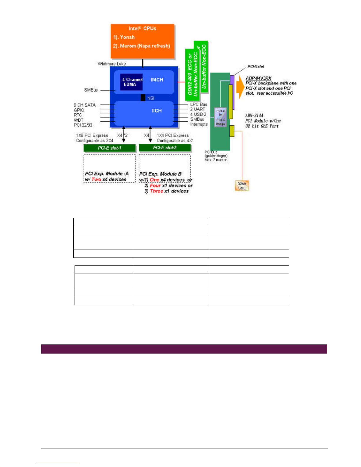
1.5 System Block Diagram....................................................................................................3
1.6 Product Specifications...............................................................................................................4
Chapter 2 Getting Started ....................................................................................................5
2.1 Included Hardware..........................................................................................................5
2.2 Before You Begin............................................................................................................5
2.3 Hardware Configuration Setting.......................................................................................6
h Location of Jumpers.........................................................................................................................6
2.4 The Chassis..................................................................................................................13
2.12 Use a Client Computer..................................................................................................14
Chapter 3 BIOS Setting .................................................................................................17
BIOS Setup Information .....................................................................................................................17
Chapter 4 Programming Guide..........................................................................................17
4.1 Reset to Default Information..........................................................................................17
4.2 ByPass WDT Programming Guide ...............................................................................38
4.3 About EZIO2 .................................................................................................................38
4.3.1 Features .....................................................................................................................38
4.3.2 Technical Support Information.......................................................................................39
4.3.3 Mechanical Specification...............................................................................................39
4.3.4 General Specification....................................................................................................39
4.3.5 Product Outlook ............................................................................................................40
4.3.6 Interface Pin Assignment...............................................................................................40
4.3.7 Hardware installation.....................................................................................................41
4.3.8 EZIO3 Function Command............................................................................................41
4.3.9 Character Generator ROM (CGROM)........................................................................................44
4.3.10 Sample Codes...............................................................................................................45
4.4 GPIO Sample Code......................................................................................................51

NAR-5620 Series User’s Manual 2
Chapter1 Introduction
1.1 AboutThis Manual
This manual contains all required information for setting up and using the NAR- 5620 series.
NAR-5620 provides the essential platform for delivering optimal performance and functionality in
the value communications appliance market segment. This manual should familiarize you with
NAR-5620 operations and functions. NAR-5620 series provide up to eight on-board Ethernet
ports to serve communication applications like Firewall, requiring ten Ethernet ports to connect
external network (internet), demilitarized zone and internal network.
NAR-5620 series overview:
Supports uPGA 479 (Socket 479) Intel® Core™2 Duo Processors.
Up to 3GB DDR2 533/667 DIMM ECC/Non-register.
Two USB ports and two COM ports
Three SATA connectors for SATA Hard disk
User-friendly LCD control panel
PCI-E architecture with totally three x1 PCI-E interfaces and two x4 PCI-E interfaces through two
PCI-E slots
Provides absolute high flexibility of customized I/O configuration for front accessible PCI-E modules
--Maximum four PCI-E x4 GbE ports + and four PCI-Ex1 GbE Ports + one PCI GbE Port.
--Optional RJ45, SFP, Bypass & Dual Personality module.
1.2 Manual Organization
This manual describes how to configure your NAR-5620 system to meet various operating
requirements. It is divided into three chapters, with each chapter addressing the basic concept
and operation of this system.
Chapter 1: Introduction. This section describes how this document is organized. It includes brief
guidelines and overview to help find necessary information.
Chapter 2: Hardware Configuration Setting and Installation. This chapter demonstrated the
hardware assembly procedure, including detailed information. It shows the definitions
and locations of Jumpers and Connectors that can be used to configure the system.
Chapter 3: Operation Information. This section provides illustrations and information on the
system architecture and how to optimize its performance.
Chapter 4: This section describes how to programming software. It includes By-pass; GPIO;
EZIO; Factory Default function.
Any updates to this manual, would be posted on the web site: http://isc.portwell.com.tw
1.3 TechnicalSupportInformation
Users may find helpful tips or related information on Portwell's web site: http://www.portwell.com.tw
A direct contact to Portwell's technical person is also available. For further support, users may
also contact Portwell’s headquarter in Taipei or local distributors.

NAR-5620 Series User’s Manual 3
Taipei Office Phone Number: +886-2-27992020
1.4 Board Layout
Figure 1-1 Board Layout of NAR-5620 M/B
1.5 SystemBlockDiagram
Figure 1-2 NAR-5620 Basic Block Diagram

NAR-5620 Series User’s Manual 4
Figure 1-3 NAR-5620 Backplane Block Diagram
System Model PCI-E Slot-1 PCI-E Slot-2
NAR-5620-0100 Optional Optional
NAR-5620-0301 Optional ABN-362 (SFP with
dual personality)
NAR-5620-0900 ABN-454 (Copper x4) ABN-434 (Copper x4)
System Model PCI-E Slot-1 PCI-E Slot-2
NAR-5622-0704 ABN-464 (SFP x4) ABN-362 (SFP with
dual personality)
NAR-5622-0900 ABN-454 (Copper x4) ABN-434 (Copper x4)
NAR-5622-0907 ABN-464 (SFP x4) ABN-434 (Copper x4)
Figure 1-4 NAR-5620 Ethernet Module
1.6 ProductSpecifications
Model: NAR-5620 series
Main Processor: Intel® μPGA 478 (Socket M) Core 2 Duo processor: Yonah/ Merom
BIOS: AMI system BIOS with 512KB flash ROM to support DMI, PnP, APM
function
Main Memory: Support 2 x 240pin DIMM sockets support DDR2 400 ECC or un-buffer Non-
ECC. p to 4GB ( 2GB DIMM).
Chipset: Intel E3100 (Whitmore Lake)

NAR-5620 Series User’s Manual 5
SATA Interface 3 x Serial ATA connectors
Serial Ports: Support two high-speed 16550C compatible UARTs with 16-byte T/R FIFOs
Support LCD/Key pad module (Portwell proprietary)
USB Interface: Support two USB2.0 ports for high speed I/O peripheral devices
Auxiliary I/O Interfaces: System reset switch, power okay LED and HDD LED interface
Power Input: Support one AC input jack (power requirement: 110V ~ 220V auto switch)
PCI Slot: One PCI slot for half-size PCI card
One PCI-X slot for half size PCI-X card
Ethernet: Ethernet configuration is depends on combination of PCI and PCI-
Express modules. Basically NAR-5620-0100 is built with ABN-214A
PCI Ethernet board, which owns one x 32bit RJ-45 GbE port. Further
PCI-Express module should be available as listed in the table below:
System Model 32b GbE Available max.
PCI-E GbE on slot-
1
Available max.
PCI-E GbE on
slot-2
NAR-5620-0100 1 4 2
NAR-5620- 1 4 4
NAR-5620-D243 1 4 4
Hardware Monitor: Support on-board hardware monitor for
System voltages: Vcore, 1.4V, +5V and +12V
Environmental
Requirements: Operating Temperature: 0°C ~ 40°C
Storage Temperature: - 20°C ~ 80°C
Relative Humidity: 5% ∼95%, non-condensing
Dimension:
Chapter2GettingStarted
This section describes how the hardware installation and system settings should be done.
2.1 IncludedHardware
The following hardware is included in package:
NAR-5620 Communication Appliance System Board
One null serial port cable
2.2 BeforeYouBegin
To prevent damage to any system board, it is important to handle it with care. The following
measures are generally sufficient to protect your equipment from static electricity discharge:
When handling the board, use a grounded wrist strap designed for static discharge elimination
and touch a grounded metal object before removing the board from the antistatic bag. Handle

NAR-5620 Series User’s Manual 6
the board by its edges only; do not touch its components, peripheral chips, memory modules or
gold contacts.
When handling processor chips or memory modules, avoid touching their pins or gold edge
fingers. Restore the communications appliance system board and peripherals back into the
antistatic bag when they are not in use or not installed in the chassis.
Some circuitry on the system board can continue operating even though the power is switched
off. Under no circumstances should the Lithium battery cell used to power the real-time clock be
allowed to be shorted. The battery cell may heat up under these conditions and present a burn
hazard.
WARNING!
1. "CAUTION: DANGER OF EXPLOSION IF BATTERY IS INCORRECTLY REPLACED. REPLACE
ONLY WITH SAME OR EQUIVALENT TYPE RECOMMENDED BY THE MANUFACTURER.
DISCARD USED BATTERIES ACCORDING TO THE MANUFACTURER’S INSTRUCTIONS"
2. This guide is for technically qualified personnel who have experience installing and
configuring system boards. Disconnect the system board power supply from its power
source before you connect/disconnect cables or install/remove any system board
components. Failure to do this can result in personnel injury or equipment damage.
3. Avoid short-circuiting the lithium battery; this can cause it to superheat and cause burns if
touched.
4. Do not operate the processor without a thermal solution. Damage to the processor can occur
in seconds.
5. Do not block air vents. Minimum 1/2-inch clearance required.
2.3 Hardware Configuration Setting
2.3.1 NAR-5620 System Board Jumper
In general, jumpers on NAR-5620 system board are used to select options for certain
features. Some of the jumpers are configurable for system enhancement. The others are
for testing purpose only and should not be altered. To select any option, cover the jumper
cap over (Short) or remove (NC) it from the jumper pins according to the following
instructions. Here NC stands for “Not Connected”.
Location of Jumpers

NAR-5620 Series User’s Manual
7
Jumper Setting:
JP7 : PCI-E x4 Configuration (Default : 2-3,5-6 / Four PCI-E x1)
JP9 : COM2 Function(Default 5-6,9-11,10-12,15-17,16-18 / RS232)
JP11: RTC CMOS Clear Jumper Setting (Default 2-3)
JP7 : PCI-E x4 Configuration
JP7 Function
1-2,4-5 One PCI-Express x4 Configuration
2-3,5-6 Four PCI-Express X1 Configuration
JP9 : COM2 RS232/485/422 Selection
JP9 Function
RS232 5-6,9-11,10-12,15-17,16-18
RS485 1-2,7-9,8-10,19-20
RS422 3-4,7-9,8-10,13-15,14-16,21-22

NAR-5620 Series User’s Manual 8
JP11 : RTC CMOS Clear Jumper Setting
JP11 Function
1-2 Clear CMOS Contents
2-3 Normal Operation
Connectors Function Description:
J1: PS/2 Keyboard/Mouse Connector
J3: 4P Power Connector for 12V Power
J4: ATX Power Connector (20 pin)
J5/J8/J18/J20/J32/J33: Fan Connector
J6: Serial Port-2 Connector
J7: Parallel Port Connector
J9: PCI-Express x8 Connector for Nic-Card used
J10: Compact Flash Socket
J12/J13/J15: SATA Interface Connector
J16: Dual Port USB Header
J17: PCI-Express x4 Connector for Nic-Card used
J19: Miscellaneous Header (Pin2-4 : Power LED, Pin1-3:HDD LED, Pin6-8: Power Button, Pin5-7: Reset Button ,
Pin9-10: Load Default Setting Button)
J21/J22/J23/J27/J28/J29/J30/J31 : PCI-Express x4 lane selection
J25: External Speaker Header
J26: Serial Port-1 Connector
J34: 8-Bit GPIO Header
J38: 80H LPC PIN Header
J1 : PS/2 Keyboard/Mouse Connector
PIN No. Signal Description
1 Mouse Data
2 N/C
3 GND
4 +5V
5 Mouse Clock
6 Keyboard Data
7 N/C
8 GND
9 +5V
10 Keyboard Clock
J3 : 4P Power Connector for 12V Power
PIN No. Signal Description
1GND
2 GND
3 +12V
4 +12V
J4 : ATX Power Connector
PIN
No. Signal Description PIN No. Signal Description

NAR-5620 Series User’s Manual 9
1 +3.3V 11 +3.3V
2 +3.3V 12 -12V
3 GND 13 GND
4 +5V 14 POWER ON SIGNAL
5 GND 15 GND
6 +5V 16 GND
7 GND 17 GND
8 ATX POWER OK 18 -5V
9 5VSB 19 +5V
10 +12V 20 +5V
J5/J32/J33 : Fan Connector
PIN No. Signal Description
1 GND
2 +12V
3 Speed Sense to SIO
J8/J18/J20 : Fan Connector
PIN No. Signal Description
1 GND
2 +12V
3 N/C
J6/J26 : Serial Port Connector
PIN No. Signal Description PIN No. Signal Description
1 Data Carrier Detect 2 Data Set Ready
3 Receive Data 4 Request to Send
5 Transmit Data 6 Clear to Send
7 Data Terminal Ready 8 Ring Indicator
9 GND 10 NC
J7 : Parallel Port Connector
PIN No. Signal Description PIN No. Signal Description
1 Strobe# 14 Auto form Feed#
2 Data 0 15 Error#
3 Data 1 16 Initialization#
4 Data 2 17 Printer Select IN#
5 Data 3 18 Ground
6 Data 4 19 Ground
7 Data 5 20 Ground
8 Data 6 21 Ground
9 Data 7 22 Ground
10 Acknowledge# 23 Ground
11 Busy 24 Ground
12 Paper Empty 25 Ground
13 Printer Select 26 N/C

NAR-5620 Series User’s Manual 10
J9 : PCI-Express x8 Connector
PIN No. Signal Description PIN No. Signal Description
B1 +12V A1 +12V
B2 +12V A2 +12V
B3 +12V A3 +12V
B4 GND A4 GND
B5 SM BUS CLOCK A5 +5V
B6 SM BUS DAT A6 +5V
B7 GND A7 +3.3V
B8 +3.3V A8 +3.3V
B9 +3.3V A9 +3.3V
B10 3VSB A10 +3.3V
B11 PCI-E WAKE Signal A11 PCI-Express RESET
Key
B12 POWER GOOD Signal A12 GND
B13 GND A13 Reference Clock (+)
B14 Transmitter differential pair Lane 0(+) A14 Reference Clock (-)
B15 Transmitter differential pair Lane 0(-) A15 GND
B16 GND A16 Receiver differential pair Lane 0 (+)
B17 WDT Clock A17 Receiver differential pair Lane 0 (-)
B18 GND A18 GND
B19 Transmitter differential pair Lane 1(+) A19 +3.3V
B20 Transmitter differential pair Lane 1(-) A20 GND
B21 GND A21 Receiver differential pair Lane 1 (+)
B22 GND A22 Receiver differential pair Lane 1 (-)
B23 Transmitter differential pair Lane 2(+) A23 GND
B24 Transmitter differential pair Lane 2(-) A24 GND
B25 GND A25 Receiver differential pair Lane 2 (+)
B26 GND A26 Receiver differential pair Lane 2 (-)
B27 Transmitter differential pair Lane 3(+) A27 GND
B28 Transmitter differential pair Lane 3(-) A28 GND
B29 GND A29 Receiver differential pair Lane 3 (+)
B30 Reference Clock (+) A30 Receiver differential pair Lane 3 (-)
B31 Reference Clock (-) A31 GND
B32 GND A32 +3.3V
B33 Transmitter differential pair Lane 4(+) A33 N/C
B34 Transmitter differential pair Lane 4(-) A34 GND
B35 GND A35 Receiver differential pair Lane 4 (+)
B36 GND A36 Receiver differential pair Lane 4 (-)
B37 Transmitter differential pair Lane 5(+) A37 GND
B38 Transmitter differential pair Lane 5(-) A38 GND
B39 GND A39 Receiver differential pair Lane 5 (+)
B40 GND A40 Receiver differential pair Lane 5 (-)
B41 Transmitter differential pair Lane 6(+) A41 GND
B42 Transmitter differential pair Lane 6(-) A42 GND
B43 GND A43 Receiver differential pair Lane 6 (+)
B44 GND A44 Receiver differential pair Lane 6 (-)
B45 Transmitter differential pair Lane 7(+) A45 GND
B46 Transmitter differential pair Lane 7(-) A46 GND
B47 GND A47 Receiver differential pair Lane 7 (+)
B48 N/C A48 Receiver differential pair Lane 7 (-)
B49 GND A49 GND

NAR-5620 Series User’s Manual 11
J10 : Compact-Flash Socket
PIN No. Signal Description PIN No. Signal Description
1 Ground 2 Data 3
3 Data 4 4 Data 5
5 Data 6 6 Data 7
7 SDCS#0 8 Ground
9 Ground 10 Ground
11 Ground 12 Ground
13 +5V 14 Ground
15 Ground 16 Ground
17 Ground 18 SA2
19 SA1 20 SA0
21 Data 0 22 Data 1
23 Data 2 24 NC
25 NC 26 NC
27 Data 11 28 Data 12
29 Data 13 30 Data 14
31 Data 15 32 SDCS#3
33 Ground 34 IOR#
35 IOW# 36 WE#
37 INT 38 +5V
39 Ground 40 NC
41 RESET# 42 IORDY
43 NC 44 REQ
45 IDEACT# 46 PDIAG#
47 Data 8 48 Data 9
49 Data 10 50 Ground
J12/J13/J15 : Serial ATA /2/3/4
PIN No. Signal Description
1,4,7 GND
2 TXP
3 TXN
5 RXN
6 RXP
J16 : Dual Port USB Header
PIN No. Signal Description
1 NC
2 VCC
3 Shield GND
4 D0-
5 D1+
6 D0+
7 D1-
8Shield GND
9 VCC
10 GND

NAR-5620 Series User’s Manual 12
J17 : PCI-Express x4 Connector
PIN No. Signal Description PIN No. Signal Description
B1 +12V A1 +12V
B2 +12V A2 +12V
B3 +12V A3 +12V
B4 GND A4 GND
B5 SM BUS CLOCK A5 +5V
B6 SM BUS DAT A6 +5V
B7 GND A7 +3.3V
B8 +3.3V A8 +3.3V
B9 +3.3V A9 +3.3V
B10 3VSB A10 +3.3V
B11 PCI-E WAKE Signal A11 PCI-Express RESET
Key
B12 POWER GOOD Signal A12 GND
B13 GND A13 Reference Clock (+)
B14 Transmitter differential pair Lane 3(+) A14 Reference Clock (-)
B15 Transmitter differential pair Lane 3(-) A15 GND
B16 GND A16 Receiver differential pair Lane 3 (+)
B17 WDT Clock A17 Receiver differential pair Lane 3 (-)
B18 GND A18 GND
B19 Transmitter differential pair Lane 2(+) A19 +3.3V
B20 Transmitter differential pair Lane 2(-) A20 GND
B21 GND A21 Receiver differential pair Lane 2 (+)
B22 GND A22 Receiver differential pair Lane 2 (-)
B23 Transmitter differential pair Lane 1(+) A23 GND
B24 Transmitter differential pair Lane 1(-) A24 GND
B25 GND A25 Receiver differential pair Lane 1 (+)
B26 GND A26 Receiver differential pair Lane 1 (-)
B27 Transmitter differential pair Lane 0(+) A27 GND
B28 Transmitter differential pair Lane 0(-) A28 GND
B29 GND A29 Receiver differential pair Lane 0 (+)
B30 Reference Clock (+) A30 Receiver differential pair Lane 0 (-)
B31 Reference Clock (-) A31 GND
B32 GND A32 +3.3V
J19 : Miscellaneous Header
PIN No. Signal Description
1 +3.3V
2 VCC Power Suspend Signal
3 HDD Power Signal
4 GND
5 GND
6 5VSB
7 Reset
8 Power On
9 Load Default
10 GND
J25 : External Speaker Header
PIN No. Signal Description
1Speaker

NAR-5620 Series User’s Manual 13
2 NC
3 NC
4 +5V
J34 : 8-Bit GPIO Header
PIN No. Signal Description
1 GPIO0
2 GPIO4
3 GPIO1
4 GPIO5
5 GPIO2
6 GPIO6
7 GPIO3
8 GPIO7
9 GND
10 +5V
J38 : 80H LPC PIN Header
PIN No. Signal Description
1 LAD0
2 +3.3V
3 LAD1
4 PCI Reset
5 LAD2
6 FRAME#
7 LAD3
8 CLOCK
10 GND
2.4 The Chassis
The system is integrated in a customized 1U chassis (Fig. 2-1, Fig. 2-2). On the front panel you
will find a 4-push-button LCD module (EZIO), right LAN ports, two USB ports and a COM port.
NAR-5620 / NAR-5620
Fig. 2-1 Front view of the chassis

NAR-5620 Series User’s Manual 14
Fig. 2-2 Rear view of the chassis
2.12 Use aClient Computer
Connection Using Hyper Terminal
If users use a headless NAR-5620 system, which has no mouse/keyboard and VGA output
connected to it, the console may be used to communicate with NAR-5620.
To access NAR-5620 via the console, Hyper Terminal is one of many choices. Follow the
steps below for the setup:
Note: Terminal software may need to update for correct console output.
1. Execute HyperTerminal under C:\Program Files\Accessories\HyperTerminal
2. Enter a name to create new dial
3. For the connection settings, make it Direct to Com1.

NAR-5620 Series User’s Manual 15
4. Please make the port settings to Baud rate 19200, Parity None, Data bits 8, Stop bits 1
5. Turn on the power of NAR-5620 system, after following screen was shown:
6. You can then see the boot up information of NAR-5620.

NAR-5620 Series User’s Manual 16
7. When message “Hit <DEL> if you want to run Setup” appear during POST, after turning on or
rebooting the computer, press <Tab> key immediately to enter BIOS setup program.
This is the end of this section. If the terminal did not port correctly, please check the
previous steps.
.

NAR-5620 Series User’s Manual 17
Chapter3 BIOSSetting
BIOSSetupInformation
BIOS (Basic Input and Output System) include a CMOS SETUP utility which allows user to
configure required settings or to activate certain system features.
The CMOS SETUP saves the configuration in the CMOS SRAM of the motherboard.
When the power is turned off, the battery on the motherboard supplies the necessary power to
the CMOS SRAM.
When the power is turned on, pushing the <Del> button during the BIOS POST (Power-On Self
Test) will take you to the CMOS SETUP screen.
When setting up BIOS for the first time, it is recommended that you save the current BIOS to a
disk in the event that BIOS needs to be reset to its original settings. If you wish to upgrade to a
new BIOS, Award BIOS utility can be used.
Awdflash allows the user to quickly and easily update or backup BIOS without entering the
operating system.
Chapter4ProgrammingGuide
4.1 Reset toDefaultInformation
; Portwell IP and Confidential
;
; By Yves Liang , 01/04/2006
; By Wayne modify, 05/22/2006
;
; Reset to default status can be read from WML(ICH7R_GPI6).
; After Power On reset, GPI6 = low ( 0 )
; If Reset to Default (RST2DF) Button pressed ( Triggered )
; ,then GPI6 will be latch to high ( 1 ).
;
; RST2DF register can be cleared by WML_GPO19 (ICH7R_GPO39.)
; Write a pulse timing ( High1_low_high2 ) to clear RST2DF to 0.
; High1 : output GPO19 high , and keep 10 us.
; Low : output GPO19 low , and keep 10 us.

NAR-5620 Series User’s Manual 18
; High2 : output GPO19 high again , and keep high always.
;
;
; Programming Guide :
; PG_Step1 : Enable ACPI IO port assignment and get PMBASE, then save to
; EBX_Bit[31..16]
;
; First : GPI_ROUT bit[13,12] P [0,0] : Let GPI6 not evoke SCI.
; Write GPI_Rout bit[13,12] to [0,0] for no effect on GPI6
; ( B0:D31:F0:Offset_B8h-Bit[13,12]P[0,0] , no SCI event evoked)
;
; Second: Enabe ACPI IO port by setting ACPI_EN bit7
; B0:D31:F0:Offset_44h_bit7P1
; Third : Get PMBASE ( ACPI I/O port BAR ) and
; save to EBX_bit[31..16].
; PMBASE=:B0:D31:F0:Offset[40..43h]
; Let Bit0 = 0.( PCI_BAR bit0 returns 1 for a IO_BAR )
;
;
;
; PG_Step2 : Enable GPIO IO function and get GPIOBASE, then save to
; ECX_Bit[31..16]
;
; How to program GPIO39 ( Output only , i.e. GPO39 )
; -------------------------------------------------------
; Get GPIOBASE =: B0:D31:F0:Offset[48..4Bh] ;(and let bit0 = 0 )
; GPIO_CNTL =: B0:D31:F0:Offset_4Ch_bit4P1 ;Enable ICH7R GPIO
;
; GPIO39
; GP_LVL (=:(GPIOBASE + 0Ch))_bit39P[0/1]; Write value 0/1
; ------------------------------------------------------
;

NAR-5620 Series User’s Manual 19
; How to read GPI6
; ======================================================
; GPI6 status MUST NOT be inverted First.
; GPI_INV (=GPIOBASE+2Ch)-bit6P0. ( GPI6 not inverted )
;
; Get GPI6 status from GPE0_STS (=PMBASE+28h)-bit22
; 0 = low , 1= high level
; ======================================================
.MODEL small ; tiny
.386
.STACK 200h
.data
PROMP1 DB'PORTWELL PPAP-3753,3753RSTD.exe, V1.00 01-04-2006,All rights reserved.$'
PROMP1_1 DB ' For PPAP-3753 Reset-to-Default test .',13,10,'$'
PROMP_2_CR_LF db 0Dh, 0Ah,0Dh, 0Ah, '$'
PROMP_Str1 db ' Reset-To-Default status latched by a F/F. ',0dh,0ah,'$'
PROMP_Str2 db ' This status bit = 0 ---> Normal. ',0dh,0ah,'$'
PROMP_Str3 db ' This status bit = 1 ---> RST2DF button has been pressed.',0dh,0ah,'$'
PROMP_Str4 db ' This status bit can be read by WML_GPI6, ',0dh,0ah,'$'
PROMP_Str5 db ' and can be cleared by an WML_GPO19 High1-Low-High2 pulse.',0dh,0ah,'$'
PROMP_Str6 db ' ',0dh,0ah,'$'
PROMP_Str7 db ' High1 = 30us High level ',0dh,0ah,'$'
PROMP_Str8 db ' Low = 30us Low level ',0dh,0ah,'$'
PROMP_Str9 db ' High2 = High level again and no level change from now on.',0dh,0ah,'$'
PROMP_StrA db ' ',0dh,0ah,'$'
PROMP_rst2df db 0dh,0ah,' Press the Reset-to-Default button and then release it for the test NOW!$'
PROMP_anykey db 0dh,0ah,' Ready? If yes, then Press any key to start test ....... $'
PROMP_err1 db 0dh,0ah,' ***** "Reset-to-Default F/F Initialization" Failed. *****',0dh,0ah,'$'
PROMP_err1_1 db ' ( This may be a H/W error or Reset-to-Default button has ever been
This manual suits for next models
5
Table of contents
Other Portwell Server manuals
Popular Server manuals by other brands

Moxa Technologies
Moxa Technologies NPort 5600-8-DTL Series Quick installation guide

Asus
Asus RS160-E5 - 0 MB RAM Configuration guide

Sun Microsystems
Sun Microsystems Sun Fire V890 Product notes

Wyse
Wyse Winterm S10 Administrator's manual

HP
HP P2000 G3 Cli reference guide

Dell
Dell PowerEdge C8000 Setup guide