QRP Labs QLG2-SE User manual

QLG2-SE
GPS/GNSS
Receiver
This manual is for the QLG2-SE GPS/GNSS Receiver module
Contents
!"#$"
%#&'()%)')*+,)-.#/
"0/
1+#"""$2""$"$34
/$##!"&"5
/!"6"7
1'###""2&"3"#$7
8
/.
40.9##&#
"":: 1

1 Introduction
The QLG2-SE GNSS (Global Navigation Satellite System) receiver module is an upgrade
over the ormer QLG1 with higher per ormance and highly lexible eatures:
QLG2-SE is a reduced unctionality version o the QLG2. Compared to QLG2, it lacks the
USB to Serial converter inter ace and the capability to use an optional LCD module.
•Multi GNSS satellite constellation receiver supports GPS (US), Galileo (Europe),
GLONASS (Russia) and Beidou (Chinese) - (de ault GPS + Beidou) - giving a aster
more accurate position ix – Module is E108-GN01 (GK9501 GNSS chip set)
•Supplied with included magnetic-mount active antenna, approx 2m coax and SMA
connectors
•Supply voltage range 3.3 to 6V.
•Board 80 x 37mm (Same as, and compatible with, Ultimate3S, VFO and Clock kits).
•Onboard LEDs or status indication: Red (Power), Yellow (Serial data) and Green
(PPS).
•2.8 to 5V logic level conversion to provide 5V serial data or ull compatibility with all
QRP Labs kits.
•Supports 2.8/3.3V logic OR 5V logic (jumper wire selected)
•SMD assembly already undertaken by actory acility - only SMA connector to solder.
•Space provided or optional ultra-capacitor or aster hot-start
All QLG2-SE GPS modules are comprehensively tested be ore shipment including:
•Active antenna with 2m coax and SMA connector unctions correctly
•Satellite reception and Time To First Fix is under 1 minute
•Serial data and 1pps outputs are correctly present
PLEASE READ THE BASIC ASSEMBLY AND USE
INSTRUCTIONS IN THIS MANUAL VERY CAREFULLY BEFORE
APPLYING POWER TO THE BOARD!
2 Getting to know your QLG2-SE
There are only THREE parts in the QLG2-SE kit:
1. 80 x 37mm PCB with assembled SMD
2. Active antenna including 2m coaxial cable and SMA connector
3. SMA connector or installation on the PCB
The parts list o the PCB is provided later in this manual in the circuit description section.
"":: 2

Kit contents:
Know your QLG2:
"":: 3

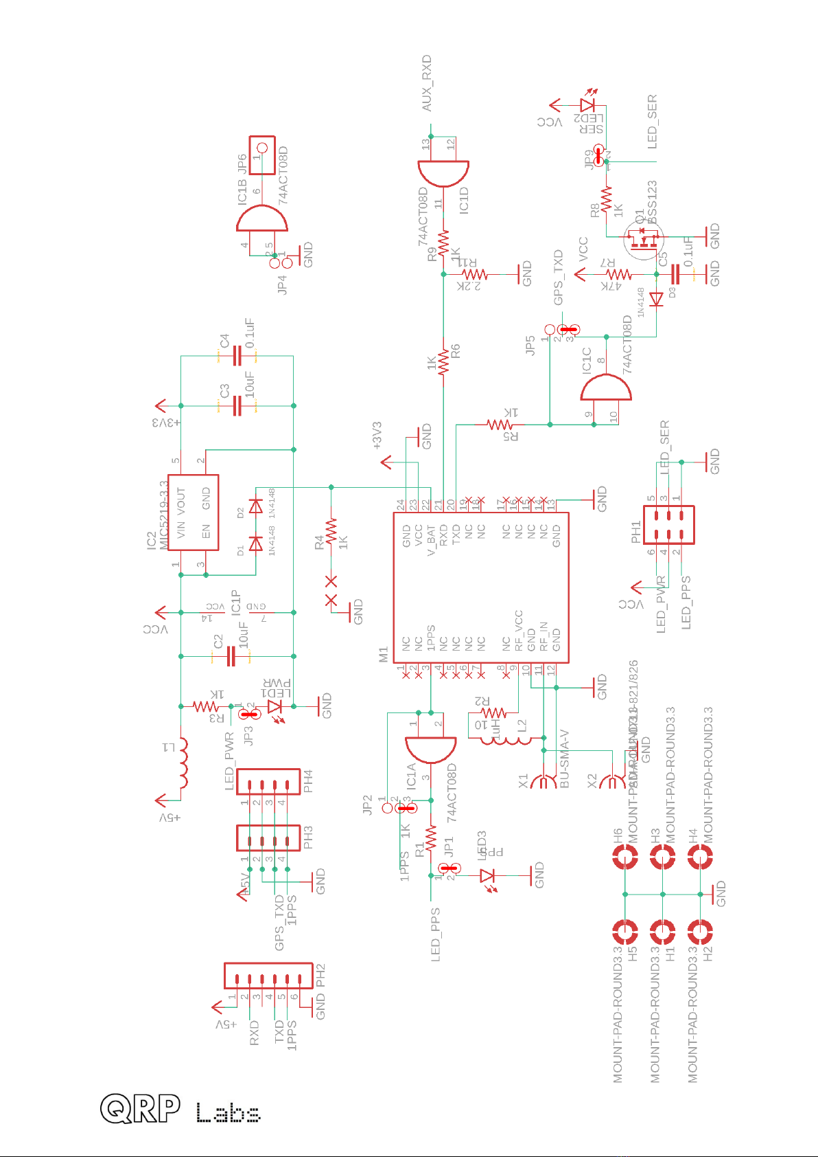
With re erence to the above photograph, looking anti-clockwise rom le t:
•GNSS Module: The E108-GN01 GNSS receiver module, multi-satellite system
capable (GPS and Beidou enabled by de ault).
•Antenna SMA Connector (supplier): Can be board edge-mounted or at 90-degrees
standing up on the board (DO refer to important assembly instructions later).
•LED enable jumpers: these are wired by de ault, and connect the signals to the
onboard LEDs. I you wanted to use external LEDs or example in a ront panel, you
would cut the tiny traces under these jumpers (see later section).
•Status LEDs:
◦Power (RED): always lit
◦Serial Data (Yellow): lashes once per second in time with the serial data burst
◦1 PPS (Blinding Green): lashes once per second when a 3D satellite lock is
acquired
•External LED connect: Three LEDs may be connected here using wires i you pre er
external LEDs to the onboard SMD LEDs.
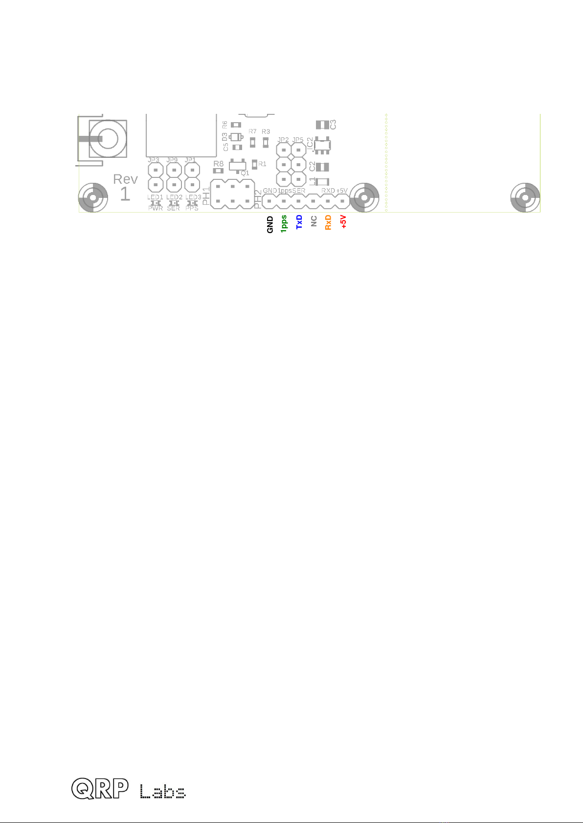
•6-pin inter ace: this provides six pads:
◦GND
◦GNSS 1pps
◦GNSS serial data
◦No connection
◦RxD serial data
◦+5V power supply input
•Option Jumpers: con igure how the serial port pads are connected, allowing either
2.8/3.3V logic or 5V logic levels
•Break-strip: this line o drilled holes allows you to easily snap o the right-hand part
o the board, i you would like a smaller board (53 x 37mm)
•4-pin inter ace: pads or QCX, U3S etc: the standard QRP Labs 4-pin connector:
+5V, Gnd, Serial Data (TxD) and 1PPS. There are two 4-pin connectors, they are
wired in parallel, so that you can use either one depending on whether or not you
break apart the PCB (see above).
•Prototyping areas – the unused space on the PCB is populated by a 0.1-inch pitch
matrix o tinned through-holes where you can add your own components i you need
to.
•Spare AND-gate: one o the our AND gates in the 74AC08 is not used, you can use
it as a bu er i you need to.
•Space or Ultracap: 5mm-spaced pads suitable or installation o an Ultracap or
ephemeris backup purposes; this provides aster hot-start.
The board size is 80 x 37mm, and the holes in the our corners are at exactly the same
positions as on the Ultimate3S, Clock and VFO kits; there ore the board can be stack-
mounted behind these kits on suitable spacers (12 or 25mm).
These eatures will be described in more detail in subsequent sections.
"":: 4

Compatibility
Straight out o the box, i you simply install the coaxial connector and plug in the antenna,
the QLG2-SE is backwardly compatible by de ault with the ormer QLG1 kit. It is there ore
directly compatible with all other QRP Labs kits:
•QCX-series CW transceivers (QCX, QCX+ and QCX-mini)
•Ultimate3S (and preceding kits in the Ultimate- series)
•Clock kit
•VFO/Signal generator kit
•ProgRock kit
3 Assembly
3 1 Assembly for basic operation
Assembly o this kit is EXTREMELY straight orward; you need only solder in the SMA
connector. This can be installed horizontally or vertically (below le t and right, respectively),
to suit your particular application.
Vertical installation: IMPORTANT! The body of the SMA
connector WILL DEFINITELY short to the center pad of the
component footprint on the board This will not only short out
the antenna, rendering it completely ine ective, it will also draw
high current rom the GNSS module through the 10-ohm
resistor R2. You will soon note the temperature rise o the
GNSS module as well as the 3.3V voltage regulator chip (you
don’t need to ask me how I know...).
Therefore it is essential to create a little gap between the
body of the SMA connector and the board
The best way to do this is via small piece o paper. It’s a simple,
cheap and e ective solution.
Cut a small piece o paper as shown (above right), place it on
the board and push the center pin o the SMA connector
through the paper.
Solder the SMA connector in place as usual. Don’t overdo the
heat and burn the paper.
"":: 5

Horizontal installation: The SMA connector happens to it the board nicely too in the
horizontal, edge-mounted position. Place it with the center pin on the top side o the board,
and two o the corner pins on the bottom side, and solder in place. The other two ground
pins can be ignored. This works very well.
3 2 Use with QCX, U3S, Clock, VFO, ProgRock etc kits
In this application, you need only plug in the antenna coax
SMA connector and the QLG2-SE is ready to use. It is
entirely compatible with the ormer QLG1 kit and the 4-way
pin header pads at the right side o the board can be used in
the same way as a QLG1 kit.
+5V power can be supplied to the module via the +5V
connection i desired.
These signals are also available on the 6-way pin header
pads at the bottom o the board edge.
3 3 Status LEDs
Just like it’s predecessor the QLG1,
the QLG2-SE module has the same
three LED status LEDs.
In the case o QLG2-SE, these are
0603-size SMD LEDs installed on
the PCB near the GNSS receiver
module.
LED 1 (red) is the Power LED and is
always lit when QLG2-SE is
powered.
LED 2 (yellow) is the Serial data
LED and pulses in time with the serial data. Note that in a departure rom the QLG1, this
LED is actually OFF during the data burst (whereas on QLG1 it is ON during the data
burst). The reasons or this are explained later, in the circuit explanation section.
LED 3 (blinding green) is the 1pps indicator and lashes once per second, or 0.1 seconds,
coincident with the 1pps pulse whose leading edge indicates the exact UT second. This
LED only starts blinking once a satellite lock (3D ix
computation) has been achieved.
Together, these three LEDs provide an accurate
diagnosis o correct operation o the QLG2-SE.
Connecting external LEDs
You may wish to use external LEDs instead o the
onboard ones. For example, you may wish to make
"":: 6

the LEDs visible on the ront panel o your equipment. A ter all, which o us does not like
blinking lights on his equipment, and generally the more the merrier.
In this case, you can connect wires at pin header PH1, as ollows in the diagram (right).
The cathodes (negative, indicated by black lines)
o the LEDs are connected to the pads nearer
the center o the board; the anodes (positive,
indicated by red lines) are connected to the pads
nearest the board edge. The sequence o the
pads, is as three pairs rom le t to right, as
Power (RED), Serial data (YELLOW) and 1pps
(GREEN) – in other words, the same order as
that o the SMD LEDs on the board.
You would also need to cut the thin exposed
tinned copper traces on the underside o the
PCB, in order to disconnect the onboard LEDs. This should be done with a sharp kni e,
care ully so as not to damage any other nearby traces.
3 4 Fitting an ultracap (a k a supercap)
There is a place on the QLG2-SE board to it an ultracap (a.k.a. supercap). This is a lot
more reliable means o providing backup power, than the little rechargeable battery on the
QLG1.
Backup power permits the operation o the internal Real Time Clock (RTC) in the GNSS
module and also retains the downloaded satellite ephemeris data, which will enable a hot-
start (satellite ix computation) within a second or two o power-up.
Most amateur radio applications will not need this, but the pads are made available on the
board in case you do wish to use it.
Be care ul to observe the correct polarity to avoid a possible bang and a nasty chemical
mess (don’t ask me how I know about this, either). The black arrows on the capacitor
body point to the negative pin
The photograph shows a 0.47 Farad, 5V capacitor installed on the QLG2 board. The
position is the same on the QLG2-SE board.
The pads are separated
by 0.2-inches (5.08mm)
and the capacitor its
per ectly. This capacitor
appears sufficient to
backup the QLG2 GPS
for at least 12 hours
"":: 7

3 5 6-pin interface header
At the center o the QLG2-SE board’s bottom edge, is a 6-pin header that provides access
to the power supply rails, the GNSS outputs, and the Serial port o the USB to Serial
converter.
The 1pps, Serial data, TXD and RXD signals can be con igured to be either 2.8V/3.3V logic
level, or 5V logic level. The con iguration is done using jumper wires that will be described
in the next section. Note that 2.8V logic will be compatible with 3.3V systems, without issue.
From le t to right:
•Power supply ground.
•1pps: 1 Pulse Per Second output rom the GNSS module; by de ault this pulse is 0.1
seconds wide and it is sent once per second. By de ault, the voltage level is 5V
which is suitable or use with QRP Labs products such as QCX, Ultimate3S, VFO,
ProgRock and Clock kits.
•TxD: The NMEA serial data output rom the GNSS module. By de ault this is at 9600
baud and is 5V logic level, which is suitable or use with QRP Labs products such as
QCX, Ultimate3S, VFO and Clock kits. Note that this signal is connected to the “TxD”
signal o the 4-pin header on the right side o the board.
•NC: This pin is not connected on QLG2-SE
•RxD: Serial data input to the GNSS module. This RxD (receive) pin is tolerant o 2.8,
3.3 or 5V logic levels and QLG2-SE automatically converts this to 3.3V or the GNSS
module.
•+5V: Power supply positive. It is nominally 5V, but in act you could power the QLG2-
SE module rom any positive supply voltage in the range 3.3V to 6.0V, and the
onboard voltage regulator will provide 3.3V to the GNSS module which is its correct
supply voltage.
NOTE that the 5V logic levels re erenced above, assume a 5V supply voltage to the QLG2-
SE; i you use a di erent supply voltage in the range 3.3V to 6.0V then the “high” logic level
will be at that di erent supply voltage, not 5.0V.
"":: 8

3 6 Interface configuration
The con iguration o the 6-pin inter ace (and indeed, the 4-pin inter ace on the right edge o
the board) is controlled by the jumper wire area above the 6-pin inter ace pin header pads.
In the de ault con iguration (speci ied by the tinned copper traces jumper wires), all outputs
are 5V logic level
In the ollowing description, the nomenclature adopted is – as illustrated in the diagram
(right):
UPPER: means the jumper wire is connected rom the center o the group o three pads, to
the top pad.
LOWER: means the jumper wire is connected
rom the center o the group o three pads, to
the lower pad.
1 PPS voltage level:
UPPER: 5V logic level (DEFAULT)
LOWER: 2.8V logic level
2 TxD voltage level (GNSS module serial data output, which is the TxD pin on the 4-pin
header at the right o the board):
UPPER: 5V logic level (DEFAULT)
LOWER: 2.8V logic level
4 Circuit diagram (schematic) and description
In the above circuit below, the position o the de ault jumper wires, which are implemented
by tinned copper traces on the PCB underside, are indicated with a thick red line.
"":: 9

"":: 10

SMD Components parts list:
Part Value Type Package
C2, C3 10uF Capacitor 0805
C4, C5 0.1uF Capacitor 0603
D1, D2, D3 1N4148 Diode SOD-323
IC1 74ACT08 IC SOIC-14
IC2 MIC5219-3.3 IC SOT23-5
L1, L2 1uH Inductor 2012
LED1 Red LED 0603
LED2 Yellow LED 0603
LED3 Green LED 0603
M1 E108-GN01 GNSS Module 16 x 12 mm
Q1 BSS123 Transistor SOT23
R1, R3, R4, R5, R6,
R8, R9
1K Resistor 0603
R2 10-ohms Resistor 0603
R7 47K Resistor 0603
R11 2.2K Resistor 0603
"":: 11

The QLG2-SE circuit is based around the E108-GN01 GNSS module. This module is
capable o reception o multiple satellite systems, not just GPS. This aids aster satellite
acquisition and higher sensitivity in di icult reception locations. The E108-GN01 module
uses the GK9501 GNSS chipset. Links to the datasheets or both o these are on the QRP
Labs QLG2-SE page http://qrp-labs.com/qlg2se
An active antenna module is used, having a magnetic mount, antenna patch and Low Noise
Ampli ier in a weather-resistant enclosure. It is supplied with 2m o coaxial cable and an
SMA connector.
Compared to the QLG1 ( ormer QRP Labs GPS module), which was already a highly
sensitive receiver, the QLG2-SE is even more sensitive.
The E108-GN01 GNSS module and the microcontroller require a 3.3V power supply; this is
provided rom the host PC over USB, or rom the host device (Ultimate3S, QCX-series
transceiver etc) which provides a 5V supply. The chosen voltage regulator is MIC5219-3.3.
The backup ultracapacitor (i installed) is charged via two 1N4148 diodes and a 1K resistor
(R4). When power to the board is removed, the ultracapacitor powers the E108-GN01’s
V_BAT pin, providing retention o the downloaded satellite ephemeris data and Real-Time
Clock. A 0.47F 5V capacitor is suitable in this application (see section above).
Level conversion rom the 2.8V output o the E108-GN01 module, to the 5V logic levels
required by other QRP Labs kits, is done using a 74ACT08 quad AND-gate chip; it is not
used as an AND gate (all gates have their two inputs tied together), it is simply used as a
logic level converter. The T in the part number 74ACT08 indicates that the device has TTL
voltage threshold compatibility, and this means a “1” (logic high) is 2.4V so it is ideally
suited or accurately converting GNSS module 2.8V logic to 5V levels.
Q1 implements a simple timer which causes the yellow LED to be extinguished whenever a
‘0’ appears on the serial signal. When the signal returns to ‘1’, the capacitor C5 must
charge up via R7, until the turn-on threshold voltage o the Q1 MOSFET is reached, at
which point the yellow LED is switched on again. This simple circuit means that the data
transmission does not directly modulate the yellow Serial data LED, the LED is only lit a
small delay a ter the end o the data burst. This avoids generating any power line noise due
to toggling the LED at 9600 baud rate, which could be radiated into sensitive radio receivers
nearby.
5 Testing
All QLG2-SE modules are tested by QRP Labs before shipping
The test includes:
•Test E108-GN01 module using the supplied active GNSS patch antenna
•Ensure time-to- irst- ix (TTFF) is under 1 minute; on a sample o 20 units, the TTFF
was ound to range rom 23 seconds to 52 seconds, with an average o 36 seconds.
•Check correct operation o Serial data and 1pps signals via status LEDs
These tests give a very high con idence that all QLG2-SE modules shipped by QRP Labs
will be in proper working order.
"":: 12

6 Resources
For updates relating to this kit please visit the QRP Labs QLG2-SE kit page http://qrp-
labs.com/ qlg2se . This web page also contains links to the E108-GN01 datasheet and the
GK9501 command re erence
For any questions regarding the assembly and operation o this kit please join the QRP
Labs group, see https://groups.io/g/qrplabs or details
7 Document Revision history
1.00 29-Jul-2020 First version or QLG2-SE
"":: 13
Table of contents