PRINCIPLES OF OPERATION
The
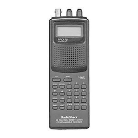
PRO
-34
is a PLL (Phase Locked Loop) syntheslzed VHF
/UHF
FM
receiver, controll
ed
by a
CPU
(centraI processing unit) via a keyboard.
The V
HF
Lo band
(30
"'-'54 MHz) or VHF
Hi
band
(136.005
"'-'174 MHz) is received
in
5 kHz increments
and
the U
HF
. Lo band
(380
"'-'5
12
MHz)
or
UHF
Hi
band
(806
"'-'960 MHz) is set up to be
12.5
kHz
increm
en
ts.. Similarly, the alrcra
ft
band
(108
"'-'136 MHz) is in a 25 kHz step.
All functions such as receivlng frequency range,frequency determination,scanning and delay time etc.
are con
tr
olled by the CPU. The
CPU
is able to do only the assigned tunetlens. and no modl
ficat
ion of the
CPU
is feasible.
The following paragraphs
ex
plain the ope
rat
ion
of
the circuit in
ter
ms
of
the functional blocks:
•
Avaractor (variabie capac
it
ance diode) tuning
("A
utomatic Tuning System") is employed
on
all Bands.
Fie
ld-eff
ect transistors (FET) are used in the RF/MIX circuits
of
low and high Bands, to achieve optim
um
mix-modulation and rnutual-rnodulatlon characteristics.
0109
amplifies the
10
.7 MHz
IF.
A
10.7
MH
z
mon
olithiccrystal
filter
is incorporated
to
ob
ta
in a good
IF
selectivity.
IC1
01
contains thelocaloscilla
tor
,mixer, IF amplifier, quadrature FM
detect
or and noise amplifier. A
crystal oscillator produces 10.
245
MHz whlch is mix
ed
with
10.7
MHz, resul
ti
ng In
455
kHz
IF.
A
45
5
kHz
ceramic
filter
Is provided to increase the IF sele
ctiv
ity
.The
455
k
Hz
IF signal is amplifled
in
the
IF
amp
stage. and the
qu
adrature
FM
detector detects It
to
an
audio signa
!.
The detected output
of
the FM Is applied
to
IC9. IC9 ampllfles the au
di
oslgnals and drives the speake
r.
•
IC1
is the
CPU
.The
CPU
does data processing, calculation etc. Any unstable supply voltage
(VDD)
to
the
CPU
can cause the
CPU
to
get mal-functloned, such as wrong data processing, wrong data transfer etc.
Ta overcome this, C2 and
R1
3 in the logic circu
it
"initia
li
ze" the CP
U.
(R
efer to the loglc section
schematic
on
page
60
.)
The lnlt
tall
zatlon
Is
done as soon as b
atte
ries or external power is connected. Flgure A shows the
inltlalizing wavefo
rm.
Memory ba
ck
up function Is automatlcally
start
ed whene
ve
rthe ini
tl
allzation has been
done
and
then tune
tl
ens
In
approxl
ma
tely 1 hour
aft
er thebatteries or extern
al
power is
dl
sconnect
ed
.
The
RESE
T switch is located in the hole on the bottom
of
the ba
tte
ry compartment and is
us
ed to
correct
an
LCD or keyboard mal-function.
The unit has battery-saving control circuit in manual mode. When the unit is in operation,the pin 74 of
IC1
(C
PU)
is
"H"
and
03
is
ON.
If no signaI input or no key input exlsted more than 5seconds in
ma
nual
mode
with the
SO
UELCH on, the pin
74
becomes
"L"
(Fig.
B)
and
03
turns
off
then the power supply for
most
of
circ
uit is shut down (except
CP
U and Audio circuit).
In
this ba
tt
er
y-s
aving
mo
de, 40% of the
power can be
sa
ve
d during normal operation.
The initialization
of
the
CPU
,mentioned above can also be done by pushing RESET switc
h.
Figure A
sh
ows the rise time duration wh
en
the
inltiallzation is done.
CX
1 (2 MHz) is a ceramic oscillator clock which is used
for
CPU
control. Figure Cshows
1/8
divided
waveform
of
Figure D.
-
5-


