Regco RG-5500 User manual

TECHNICAL
MANUAL
RG·5500
VHF/UHF
RECEIVER
specialists
in
electronic
equipment
and
systems
"
The
R.
E.
GRIMM COMPANY
16000
Industrial Drive
Gaithersburg, Maryland
20760
Courtesy of http://BlackRadios.terryo.org

·
FEBRUARY
1981
-dlE-
Vl$ION
A
RG-5500
VHF/UHf
RECEIVER
TECHNICAL
MANUAL
Courtesy of http://BlackRadios.terryo.org

INTRODUCTION
This
manual
provides
information
on the
operation
and Maintenance of the
RG
-5500 VHF
/UHF
Receiver.
Parts
lists
and a
complete
set
of
schematic
drawings
are
included.
Chapter
1,
Description
of
Equipment,
presents
a
physical
and
functional
description
of
the
receiver
. A complete
list
of
specifications
is
also
provided.
Chapter 2,
Installation,
deae
rtbes
equipment
inspection,
mounting, and
installa-
tieD
procedures.
All
rear-panel
controls
and
connectors
are
described.
Chapter
3.
Operation,
identifies
all
front-panel
controls,
indicators,
and
connectors
and
describes
procedures
for
receiver
operation.
Chapter
4,
Principles
of
Operation,
functionally
describes
the
operation
of
the
receiver,
keyed to
block
and
schematic
diagrams
.
Chapter
5, Alignment,
describes
alignment
proced
u
res
and
operational
checks.
Chapter
6,
Parts
Lists.
itemizes
the
electrical
components,
integrated
ci
rcuit
modules.
and
electro-mechanical
parts
referenced
to
layout
diagrams.
Chapter
7.
Drawings,
contains
interconnection,
power.
and
schematic
diagrams.
A
table
listIng
signal
mnemonics
is
also
included
.
Chapter
8.
Integrated
Circuit
Data,
lists
and
descrlbes
all
Integrated
circuits
used
in
the
receiver.
(il
blank)
Courtesy of http://BlackRadios.terryo.org

TABLE
OF CONTENTS
Chapter
INTRODUCTION
LIST
OF
ILL
USTRATIONS
LIST
OF
TABLES
1.
DESCRIPTION
OF
EQUIPMENT
1
-1.
INTRODUCTION
1-2
. PHYSICAL DESCRIPTION
1-3.
SPEC
IFIC
ATIONS
1-4.
FUNCTIONAL DESCRIPTION
2. INSTALLATION
2- 1.
PRELIMINARY
CHECKS
a. Inspection
b.
AC
Voltage
Check
c.
Rece
i
ver
Remote Control
Address
Set
2
-2.
OPERATIONAL
CHECKS
2-
3.
INSTALLATION
AND
MOUN
TI
NG
3.
OP
ERATION
3
-1.
CONTROLS, INDICATORS, AND CONNECTORS
3- 2.
OPERATING
PROCEDURES
a. Local Mode Operation
b. Memory Mode Operation
c. Remote Mode Operation
(1) Remote
Address
ing
the
Receiver
(2) Command
Format
d. Spectrum. Monitor
4.
PRINCIPLES
OF
OPERATION
4
-1.
INTRODUCTION
4- 2.
SIMPLlFIED
FUNCTIONAL
DESCRIPTION
a.
Digital
Control
Section
b.
Synthesizer
Section
c.
RF
Section
d.
AGe
Section
e.
IF
Section
Page
vi
x
i-I
1-1
1-1
1-6
2-1
2- 1
2-1
2-1
2- 2
2- 2
3-1
3-1
3-1
3-2
3-2
3
-2
3-2
3-4
4- 1
4
-1
4-1
4-1
4-1
4-2
4- 2
ill
Courtesy of http://BlackRadios.terryo.org

TABLE
OF
CONTENTS -
Continued
Ch
apter
Page
4-3.
DETA
I
LED
FUNCTIONAL
DESCRIPTION
4-3
a.
Digital
Control Section 4- 2
(1) Di
gital
Control
Assemb
ly
4-2
(2) Remote Control Interface
Assembly
4- 4
b.
Synthesi
zer
Section
4-5
(1
)
A22
Synthesizer
Assembly
(figu
re
7- 15)
4-5
(2) A20 and
A2
1 Voltage
Contl'O
ll
ed
Osc
ill
ators
4-9
c. RF Section. 4- 9
(1) A33
RF
Input Switch
(figure
7-59)
4- 9
(2) A16
RF
Assemb
ly (figu
re
7-13)
4-
10
(3) AlB
RF
Preselector
Driver
and PIN Diode
Switch
Olivers
(figure
7-14)
4-11
d.
AGe
Section
4-11
(1) A25 AGC
Amplifier
(figure
7-51)
4- 11
(2) A28
COR/Squelch
Amplifier
(figure
7-54)
4- 12
e.
IF
Section
4-12
(1) A23 IF
Assembly
(figure
7- 27) 4- 12
(2) A27 Audio
Video
Amplifier
(figure
7- 53)
4-14
4-4.
POWER
SUPPLY
CIRCUITS
4-14
4-5.
A24
SPECTRUM
MONITOR
(figure
4-8)
4-
14
a. A24A2 Amplifier, Mixer, IF Ampl
ifier
(
fi
gure
7-
46) 4- 14
b.
A24A3 Sweep
Generator/VeO/Marker
(figu
re
7-47)
4-15
c.
A24A5
Deflection
Amplifier
(figu
re
7
-4
9)
4-15
d.
A24A4
DC/DC
Converter
(figure
7-48)
4-
15
5.
ALIGNMENT
5-
l.
INTRODUCTION
5-1
5- 2.
TEST
EQUIPMENT
5- 1
5-
3.
RECEIVER DISASSEMBLY AND
REASSEMBLY
5- 1
5-4.
POWER
SUPPLY
VOLTAGE CHECKS
5-1
5- 5. A34 AND A35
FIRST
AND
SECOND
LOCAL
OSCILLATOR
AMPLIFIER
OUTPUT
CHECK 5-2
5- 6. A23A5
IF
ASSEMBLY
OUTPUT
AMPLIFIER
ALIGNMENT
PROCEDURES 5- 3
a. A23A5 Output
Amplifier
5- 3
b.
Beat
Frequency
Oscillator
5- 5
5- 7.
A23AI
-A4
IF
ASSEMBLY
21.4
MHz
BANDPASS
AMPLIFIERS
5- 5
Iv
Courtesy of http://BlackRadios.terryo.org

TABLE
OF
CONTENTS -Continued
Chapter
Page
5-
8.
A23A6
-A9
IF
ASSEMBLY 21.4 MHz
LIMITER/DISCRIMINATORS 5-8
5
-9
. A25 AGC ASSEMBLY ALIGNMENT
5-11
5-10.
RF
TONER
SECTION ALIGNMENT
5-11
5-11.
A24A2
SP
ECTRU
M MONITOR
AMPL/MIXER/IF
AMPL
5-14
A24A3
SPECTRUM
MONITOR
SWEEP
GEN/VCO/MKR
5-18
5
-1
3. A24A5
SPECTRUM
MONITOR
DEFLECTION
AMPLIFIER
5-20
6.
PARTS
LIST
7. DRAWINGS
7-1.
INTRODUCTION
7
-2.
SIGNAL MNEMONICS
8. INTEGRA
TED
CIRCUIT DATA
8
-1.
INTEGRA
TED
CIRCUIT LOGIC SYMBOLS
8- 2. INTEGRA
TED
CIRCUIT LOGIC DIAGRAMS
7-1
7-1
8
-1
8
-1
v
Courtesy of http://BlackRadios.terryo.org

Figure
1-l.
1-2.
1-
3.
2-
l.
2-2.
3
-1
.
4
-l.
4-2
.
4-
3.
4-4.
4- 5.
4-6.
4-7.
4-8
.
5
-l.
5-2
.
5-3.
5-4
.
5-
5.
5-6.
5-7.
5- 8.
5-9.
5
-10.
5-
11.
5- 12.
5
-1
3.
6-l.
6-2.
6-3.
6-4.
6-5
.
6- 6.
6-7.
vi
LIST OF ILLUSTRATlONS
RG
-5500
VHF
/UHF
Re
c
eiver
RG-5500
Ass
e
mbly
Locations
Titl
e
RG-5500 VHF/
UHF
Receiver
Simplified
Block
Diagram
Remote Control Address Switch Selection
Rear Panel Controls and Connectors
Front Panel Controls, Indicators,
and
Connectors
RG-5500
Receiver
Functional Block Diagram
Digital
Co
nt
rol
Assemb
ly Functional
Block
Diagram
Remote Control Interface
Assembly
Functional Block Diagram
Synthesizer
Section Functional Block Diagram
RF TUner Section Functional Block Diagram
AGC
Section Functional BlockDiagram
IF
Amplifier
Section Functional Block Diagram
A24 Spectrum Monitor Functional
Block
Diagram
A23A5 21. 4
MHz
Output Amplifier Alignment
Test
Setup
A23A5
21.4
MHz
Output
Amplifier Frequency Response
Test
Setup
A23
IF
Assembly
Adjustment Locations
A23AI-A4 21. 4
MHz
Bandpass Amplifier Frequency Response
Alignment
Test
Setup
Typical Bandpass Amplifier Response Curve
A23AI-A4 21. 4
MHz
Bandpass Amplifier Gain
Adj
u
st
Test
Setup
A23A6-A9 21. 4
MHz
FM
Limiter/Discriminator
Frequency
Response Alignment
Test
Setup
A23A6-
A9
21. 4
MHz
FM
Limiter/Discriminatol'
Gain Adju
st
Test
Setup
AGC
Assembly,
RF
Section,
and
Spectrum Monitor
Ad
justment
Locations
A24 Spectrum Monitor Bottom View Adjustment and
Test
Point Locations
A24 Spectrum Monitor 21. 4
MHz
Inpu
t Amplifier Alignment
Test
Set
A24 Spectrum Monitor
13
MH
z
IF
Amplifier Alignment
Test
Setup
A24
Spectrum Monitor 2
MH
z IF Amplifier Alignment
Test
Setup
RG-5500 VHF/
UHF
Receiver
Component Locations
Rectifier
Board
Al
Parts Location Diagram
Control Circuit
Power
Supply
A2
Parts
Location Diagram
Switch Boa
rd A7 Parts
Lo
cation Diagram
Display
Register
AS Parts Location Diagram
Display
Driver
A9
Parts Location Diagram
Display Board AIO
Parts
Location Diagram
Page
1-0
1-7
1-9
2-4
2- 5
3- 5
4-17
4-19
4-21
4-23
4-25
4-27
4-29
4-
31
5-3
5-4
5-6
5-7
5-9
5-9
5-12
5-12
5-13
5-15
5-17
5-
17
5
-1
8
6-11
6-23
6-25
6-27
6-
29
6-31
6-33
Courtesy of http://BlackRadios.terryo.org

Figure
6-8.
6-9.
6-10.
6-11.
6-12.
6
-1
3.
6-14.
6-15.
6-16.
6-17.
6-18.
7-1.
7-2.
7-3
.
7-4.
7-5.
7-6.
7-7.
7-
8.
7-9.
7-10.
7-1I.
7-12.
7-13.
7-14.
7-15.
7-16.
7-17.
7-18.
7-19.
7-20
.
7-21.
7-22.
7-23.
7-24
.
LIST
OF
ILLUSTRATIONS -
Continued
Title
Memory Board
All
Parts Location Diagram
Hold
Register
A12
Parts
Location Diagram
I/O
Board
Al3
Parts
Location Diagram
Remote Control I/O Board A14
Parts
Location Diagram
Remote Control Interface
A15
Parts
Location Diagram
RF
Preselector
Oliver
and
Pin Diode Switch
Drivers
Al8
Parts
Location Diagram
AGC
Amplifier A25
Parts
Location Diagram
Audio/Video Amplifier
A27
Parts
Location Diagram
COR/Squelch Amplifier
A28
Parts Location Diagram
Trigger
Generator A32 Parts Location Diagram
RF
Input
Switch A33
Parts
Location Diagram
RG-5500 VHF/UHF
Receiver
Main
Chassis
Schematic Diagram
RG-5500 Main Power Schematic Diagram
A 1
Rectifier
Board Schematic Diagram
A2
Control Circuit Power Supply Schematic Diagram
A8
Display
Register
Schematic Diagram
A9
Display
Driver
Schematic Diagram
AID
Display
Board Schematic Diagram
A
11
Memory Board Schematic Diagram
A
12
Hold
Register
Schematic Diagram
A
13
I/o
Board Schematic Diagram
A14 Remote Control I
/O
Board Schematic Diagram
A
15
.Remote Control Interface Schematic Diagram
A
16
RF
Tuner Module Schematic Diagram
A
18
RF
Pl'eselector
Drivers
and
PlN Diode Switch
Drivers
Schematic Diagram
A22
Synthesizer
Assembly
Schematic Diagram
A22Al
Iterative Synthesizer Schematic Diagram
A22AlAl
Filter
Module Schematic Diagram
A22A2, A3.
A4
Iterative Synthesizer Schematic Diagram
A22A5
Base
Synthesizer Schematic Diagram
A22A6
Reference
Generator Schematic Diagram
A22A7 Steering Synthesizer Schematic Diagram
A22A8 Output Tracking Synthesizer Schematic Diagram
A22A9
138.600
MHz
Phase-Locked Local
Oscillator
Schematic Diagram
A22A10 638
.6
00 MHz
Phase-Locked
Local
Oscillator
Schematic Diagram
6-35
6- 39
6
-4
2
6-47
6-50
6-69
6-207
6-216
6-220
6-228
6-230
7-5
7-11
7-13
7-15
7-17
7-19
7-21
7-23
7-25
7-
29
7-31
7-33
7-37
7-3
9
7-41
7-43
7-
45
7-47
7-49
7-51
7- 53
7-55
7-57
7-59
vii
Courtesy of http://BlackRadios.terryo.org
Figure
7-25
.
7-26
.
7-27.
7- 28.
7-29.
7- 30.
7-31.
7-32
.
7-
33.
7-34.
7-35.
7-36.
7-37.
7- 38.
7- 39.
7-
40.
7-41.
7-42.
7-43.
7-44.
7-
45.
7-
46.
7-47.
7-48.
viii
LIST
OF
ILLUSTRATIONS -
Continued
Title
A22A10Al
Frequency Multiplier Module
Schematic
Diagram
A22All
2ND
LO
Switch Schematic
Diagram
A23 IF
Assembly
Schematic Diagram
A23A
1-
A4
21.
4
MHz
Bandpass
Amplifier
10 kHz to 100 kHz
Bandwidth Schematic Diagram
A23AI-A4
21.4
MHz
Bandpass
Amplifier
300
kHz
Bandwidth
Schematic
Diagram
A23A1-A4
21.4
MHz
Bandpass
Amplifier
500 kHz Bandwidth
Schematic
Diagram
A23A1-A4
21.
4
MHz
Bandpass
Amplifier
1
MHz
Bandwidth
Schematic
Diagram
A23A1-A4 21. 4
MHz
Bandpass Amp
lifier
2 MHz Bandwidth
Schematic
Diagram
A23A1-A4 21. 4
MHz
Bandpass Amplifi
er
3
MHz
Bandwidth
Schematic
Diagram
A23AI
-A4
21.
4
MHz
Bandpass
Amplifier
4
MHz
Bandwidth
Schematic
Diagram
A23A5
21.4
MHz
Output
Amplifier
and
AM
Detector
Schematic
Diagram
A23A6-A9
21.
4
MHz
limiter/Discriminator
10 kHz
to
100 kHz
Bandwidth Schematic
Diagram
A23A6-A9
21. 4 MHz
Limiter/Discriminator
300 kHz Bandwidth
Schematic
Diagram
A23A6-A9
21. 4 MHz
Limiter/Discliminator
500 kHz Bandwidth
Schematic
Diagram
A23A6-A9 21. 4
MHz
Limiter/Discriminator
1
MHz
Bandwidth
Schematic
Diagram
A23A6-A9 21
.4
MHz
Limiter/Discriminator
2 MHz Bandwidth
Schematic
Diagram
A23A6-A9 21. 4
MHz
Limiter/Discliminator
3
MHz
Bandwidth
Schematic
Diagram
A23A6-A9 21. 4
MHz
Limiter/Discriminator
4
MHz
Bandwidth
Schematic
Diagram
A23A10 IF Switching Module Schematic
Diagram
A24
S{JElctrum
Monitor Schematic
Diagram
A24A1
Input
Filter
Schematic
Diagram
A24A2
Amplifier/Mixer/IF
Amplifi
er
Schematic
Diagram
A24A3 Sweep
Generator/VeO/Marker
Schematic
Diagram
A24A4 DC/DC
Converter-Focus
and Intensity
Assembly
Schematic
Diagram
Page
7-61
7-63
7-65
7- 67
7-69
7-71
7-73
7-75
7-77
7-79
7-81
7-83
7-85
7-87
7-89
7-91
7-93
7-
95
7-97
7-99
7-101
7-103
7-107
7- 111
Courtesy of http://BlackRadios.terryo.org
LIST
OF
ILLUSTRATlONS -Cont
inued
Figure
Title
Page
7-
49.
A24A5
Deflection
Amplif
i
er
Schematic
Diagram. 7
-11
3
7
-5
0. A24A6
Power
Regulator
Schematic
Di
agram
7-11
5
7-5l.
A25
AGe
Amplifier
Sc
hematic Diagram
7-
117
7- 52. A26 21. 4 MHz
Line
Amp
lifi
er
Schematic
Di
agram
7-119
7-53.
A27
Audio/Video
Amp
lifi
er
Schematic
D
iag
ram
7
-1
21
7
-5
4.
A28
COR/Squelch
Amplifier
Schematic
Diagram
7
-1
23
7- 55. A29 Phone
Jack
Assemb
ly
Schematic
Diagr
am
7-
125
7-56.
A30 Output
Filter
Assembly
Schema
ti
c
Diagram
7- 127
7
-57.
A3!
COR
Relay
Assembly
Schem
atic
Diagram
7
-1
29
7-58.
A32
Trigger
Generator
Schematic
Di
agram
7-131
7-59.
A33
RF
Input Switch Schematic Diagram 7
-1
33
7-
60.
A34 2ND LO
Amplifier
Schematic
Diagram
7-135
7-6l.
A35 1ST LO
Amplif
i
er
Schematic
Diagram
7-137
8
-l.
Integrated Cir
cuit
Logic
Symbols and
Truth
Tabl
es
8-3
8-2.
Integrated C
ir
cllit
Logic
Diagrams
8- 5
ix
Courtesy of http://BlackRadios.terryo.org
Table
2-I.
3-I.
5
-I.
6-I.
6-2.
6-3.
6-4.
6-5
.
6- 6.
6-
7.
6- 8.
6-
9.
6
-1
0.
6- 11.
6- 12.
6-13.
6-14.
6
-15.
6- 16.
6-17.
6
-1
8.
6
-19.
6
-2
0.
6-
2l.
6-
22
.
6-23.
6-24.
6-
25.
6-26.
6-
27.
6- 2
8.
6- 29.
6-
30.
6-3l.
6-32.
6- 33.
6-34.
6- 35A.
x
LIST
OF
TABLE
S
Ti
tl
e
Rear
Panel
Controls and Indicators
Front
Panel
Contl"o
l
s.
Indicators, and Connecto
rs
Rece
i
ver
AM, FM,
Sensitivity
in
-dBm
at Given
IF
Bandwidths
RG-5500
VHF/UHF
Receiver
Parts
List
Rectifier
Board
Al
Parts
List
Control Circuit
Power
Supply A2
Parts
List
Switch
Board
A7
Parts
List
Display
Register
AS
Parts
List
Display
Driver
A9
Parts
List
Display
Board AlO
Parts
List
Memory
Board
All
Parts
Lis
t
Hold
Register
A12
Parts
List
I/o
Board
Al3
Parts
List
Remote
Control I/o Board A14 Parts
List
Remote Control Interface A15
Parts
List
RF Tuner Module A16
Parts
List
Second
Converter
Switch A16Al
Parts
List
High Band
Preamplifier
No. 2
Al6A2
Parts
List
First
Converter
Switch A16A3
Parts
List
Low Band
Preamp
l
ifier
and Switch
A16A4
Parts
List
High Band Pr
eamplifier
No. 1 A
l6A5
Parts
List
RF
Preselector
Driver
and Pin Diode Switch
Drivers
AlB
Parts
Li
st
Synthesizer
Assem
bl
y A22
Parts
List
It
erative
Synthesizer
A22Al
Parts
List
Filter
Module
A22AlAl
Parts
List
I
terative
Synthesizer
A22A2,
A3,
A4
Parts
List
Base
Synthesizer
A22A5
Parts
List
Reference
Generator A22A6
Parts
List
steering
Synthesi
zer
A22A7
Parts
List
Output Tracldng
Synthesizer
A22AS
Parts
List
13
8.600
MHz
Phase
-L
ocked
Crystal
Osci
lla
tor
A22A9
Parts
List
63S. 600
MHz
Phase
-L
ocked
Local
Osci
ll
ator
A2ZA
lO
Parts
List
Frequency
MultiplierModule A22AlOAl
Parts
Lis
t
X10 Mu
ltipli
er
A22A10AIAI
Part.
Li
st
RF
Amplifier
A22AIOA1A2
Parts
List
2ND
LO
Switch
A22All
Parts
List
IF
Assemb
ly A23
Parts
List
21.
4
MHz
Bandpass
Amplifier
A23Al
-A4
(10 kHz to 100 kHz
Bandwidth)
Parts
List
Page
2-3
3-6
5-10
6-12
6-
24
6-26
6-
28
6- 30
6-32
6-34
6- 36
6-40
6-43
6-
48
6-51
6-55
6-59
6- 62
6- 63
6-65
6-67
6
-7
0
6- 73
6
-7
6
6-82
6- 83
6-89
6- 93
6-96
6-100
6-106
6-112
6- 118
6-119
6- 122
6- 124
6- 125
6
-1
28
Courtesy of http://BlackRadios.terryo.org
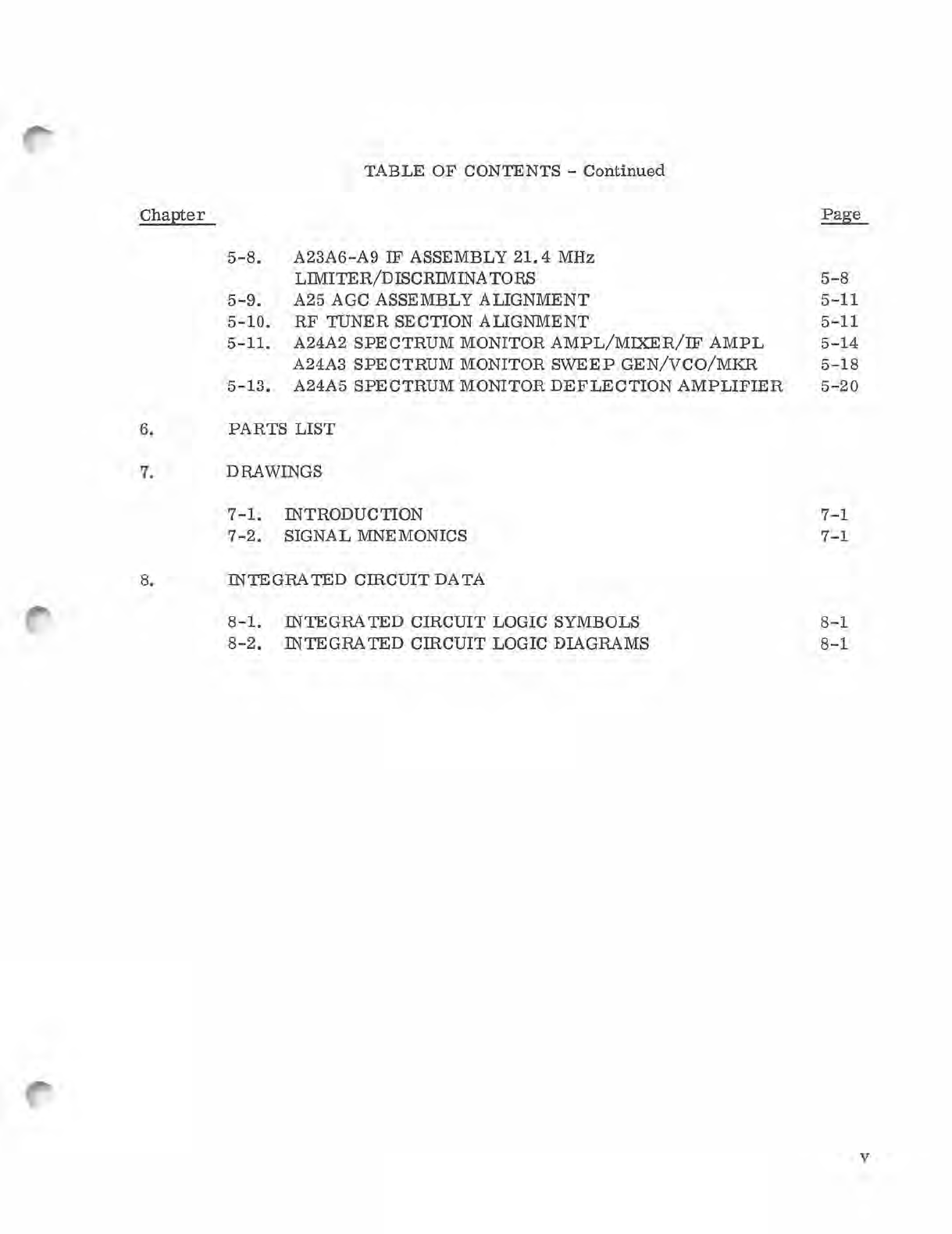
Table
6-3SB.
6-3SC.
6-35D.
6-35E.
6-3SF.
6-35G.
6-36.
6-37A.
6-37B.
6-
37C.
6-37D.
6-
37E.
6-37F.
6-37G.
6-38.
6-39.
6-40.
6-41.
6-42.
6-43.
6-44.
6-45
.
6-46.
6-47.
6-48.
6-49.
6
-S
0.
LIST
OF
TABLES
-
Continued
Title
21.
4 MHz
Bandpass
Amplifier
A23A1-A4
(300 kHz
Bandwidth)
Parts
List
21.4
MHz
Bandpass
Amplifier
A23Al-A4
(500 Hz
Bandwidtb)
Parts
List
21.4
MHz
Bandpass
Amplifier
A23A1-A4
(1
MHz
Bandwidth)
Parts
List
21.
4 MHz
Bandpass
Amplif
i
er
A23AI-A4
(2
MHz
Bandwidth)
Parts
List
21. 4 MHz
Bandpass
Amp
l
ifier
A23A1-A4
(3
MHz
Bandwidth)
Parts
List
21.
4 MHz
Bandpass
Amplifier
A23A1-A4
(4
MHz
Bandwidth)
Parts
List
21.
4 MHz Output
Amplifier
and
AM
Detector
A23A5
Parts
List
21. 4 MHz
Limiter/Discriminator
A23A6-A9
(10 kHz to 100 kHz
Bandwidth)
Parts
List
21.
4 MHz
Limiter/Discriminator
A23A6-A9
(300
kHz
Bandwidtb)
Parts
List
21.
4 MHz
Limiter/Discriminator
A23A6-A9
(500 kHz Bandwidth)
Parts
Lis
t
21.
4 MHz
Limiter/Discriminator
A23A6-
A9
(1
MHz
Bandwidth)
Parts
List
21.
4 MHz
Limiter/Discriminator
A23A6-A9
(2
MHz BandWidth)
Parts
List
21.
4
MHz
Limiter/Discliminator
A23A6-A9
(3
MHz
Bandwidth)
Parts
List
21.
4 MHz
LImIter/Discrtminator
A23A6-A9
(4
MHz
Bandwidth)
Parts
List
IF
Switching
Module A23A10
Parts
List
Spectrum
Monitor A24
Parts
List
Input
Filter
A24A1
Parts
List
Amplifier/Mixer/IF
Amplifier
A24A2
Parts
Ust
Sweep Generator/VCO/Marker A24A3
Parts
List
DC/DC
Converter-Focus
and
Intensity
Assembly
A24A4
Parts
List
Deflection
Amplifier
A24A5
Parts
List
Power
Regulator A24A6
Parts
List
AGe
Amplifier
A25
Parts
List
21.
4
MHz
Line
Amplifier
A26
Parts
List
Audio/Video
Amplifier
A27
Parts
List
COR/Squelch
Amplifier
A28
Parts
List
Phone Jack
Assembly
A29
Parts
List
Page
6- 131
6-135
6- 139
6-143
6-147
6-151
6-155
6-161
6- 164
6-167
6
-170
6- 173
6-176
6-
179
6- 182
6-185
6-188
6- 189
6-195
6-201
6
-2
04
6
-2
06
6-208
6
-21
4
6-217
6-221
6-224
Courtesy of http://BlackRadios.terryo.org
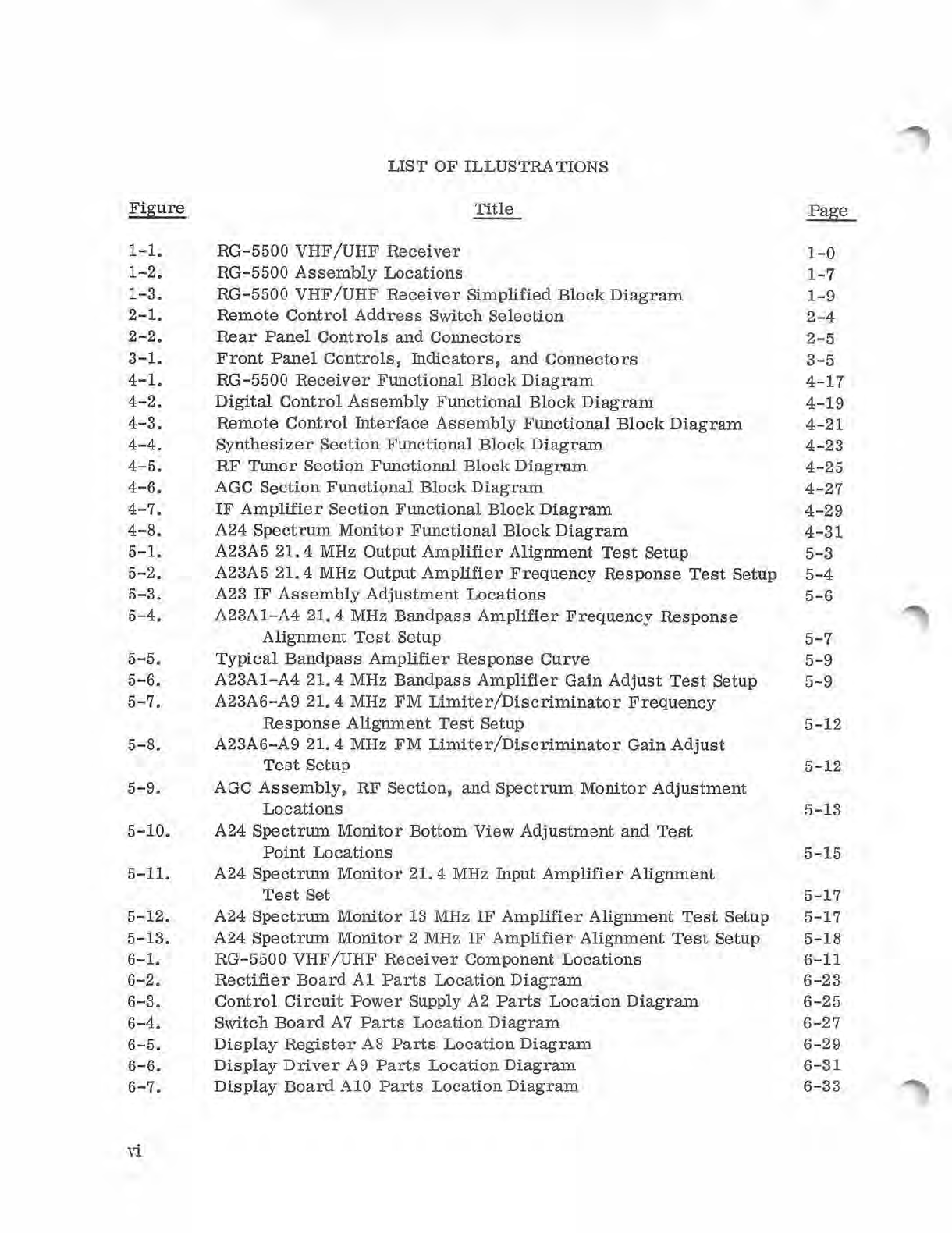
LIST
OF
TABLES
-
Continued
Table
--
TiUe
Page
6-51. Output
Filter
Assembly
A30
Parts
List
6-225
6- 52. COR
Relay
Assemb
ly A31
Parts
List
6- 227
6-53.
Trigger
Generator A32
Parts
List
6-
229
6-54.
RF
Input
Switch
A33
Parts
List
6-231
6- 55. 2ND
La
Amplifier
A34
Parts
List
6-232
6
-56.
1ST
LO
Amp
lif
ier
Module
ASS
Parts
List
6-233
7-1.
Signal Mnemonics
7-1
xii
Courtesy of http://BlackRadios.terryo.org
....
,
a
~~dt
,
'..
...
"
...
'
[J
,.,
....
,
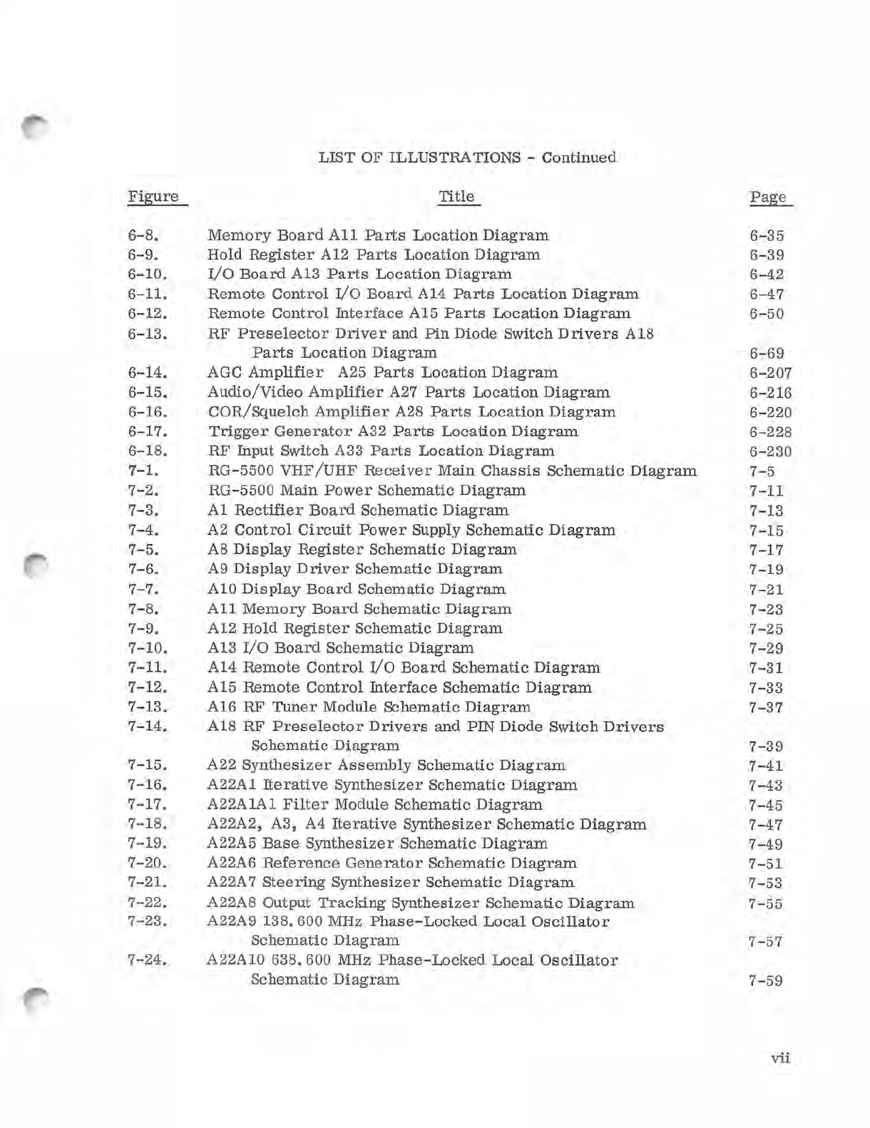
Figure 1
-1.
RG-5500 VHF/ UHF Re
ce
i
ver
Courtesy of http://BlackRadios.terryo.org

CHAPTER
1
DESCRIP
TI
ON
OF
EQUIPMENT
1- 1. INTRODUCTION.
The
RG-5500
VHF/UHF
Receiver
(figure
1-
1)
is
a fully
synthesized,
digitally controlled,
solid-state
receiver.
The
receiver
operates
in tbe
range
of
20
to
1000
MHz, and
provides
AM
, FM,
CW,
and Pul
se
reception
with a
resolution
of 100 Hz. The
receiver
is
contro
ll
ed
by
either
t
he
local,
remote
,
or
memory
modes
of
operation
provided, with
the
front panel
display
indicating the
status.
Four
IF
bandwidth options
are
selected
in addition to an optional
sp
ectr
um
monitor
unit.
1-
2.
PHYSICAL
DESCRIPTION.
The
RG
-5500
VHF
/
UHF
Receiver
mounts
in
a
standard 19-incb equipment rack and has a panel height
of
5 1/ 4-
incbes.
The RF, IF,
synthesizer.
and
digital
co
ntrol
assemblies
together with the
AGe
section
, power
supply, and optional
spectrum
monitor
are
located
in
the
receiver
top portion
(figure
1-2)
. The
remote
control
interface
assembly
and
battery
supply
are
located
in
the bottom portion. All input
/o
utput
co
nnectors,
including the
24-pin
remote
con-
trol
connection,
are
located
on the
chassis
rear
panel.
These
connections
are
described
in
chapter 2.
All
operator ac
ce
ssable
con
trols
and
connectors
are
located
on
the
chassis
front panel, and
are
described
in
chapter 3.
1-3.
SPECIFICATIONS.
Specifications
for
the
RG-5500
VHF/UHF
Receiver
are
as
follows:
Characteristics
Frequency
Range . .
.......
..
.
..
...
. .
..•
Frequency
Resolution
.................
RF
Input
Impedance
............
..
.
..
RF
Input
VSWR ..........
..
..........
RF
Input
Noise
Figure
................
Specification
20
to
999.9999
MHz
100 Hz
50
ohms,
nominal
2. 5:1.
maximum
from 20 to 5
10
MHz;
3.
0
:1,
maximum
from
510
to 1000
MHz
8
dB,
maximum from 20 to
510
MHz;
10
dB,
maximum
from
510
to 1000
MHz
1-1
Courtesy of http://BlackRadios.terryo.org
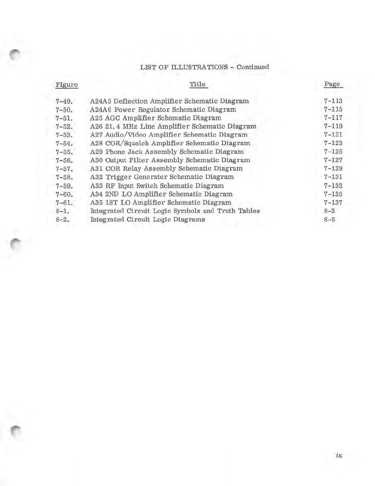
Intermodulation
Intercept
Points
:
2nd
Order
,
in
-
band
referenced
to
RF
Input
.
.....
..
.•......
....
. . .
...••
3rd
Order,
in-band
refere
n
ced
to
RF
Input .
..
.
.....
.
.......
....
...
...
.
RF
Input
Dynamic
Range
........
.
...
•.
..
Synthesizer
Step
TIme
External
Reference
Standard
Input
Frequency
Source
•..
....•.
.....
. •.
.•
.
..
Image
Rejection
..
..
...........
.. ..
...
Residua
l
AM
..
..
..
........
.
..
...
...
...
Predetectio
n
IF
Ou
tput
............
..
...
Internally
Generated
Spurious
•
....
.
...
. .
Gain
Co
ntr
ol Modes .
.......
....
•.
.....
.
AGe Stability
1-2
o dBm.
no
minal
-10
dBm,
nominal
From
maximum
sensitivity
of
recei
ver
to - 5
dBm
Less
t
han
100
microseconds
per
step
5 MHz, 0
dBm
nominal
into
50
ohms
,
rear
panel
access
85 dB, minimum.
from
20
to 510
MHz;
60
dB,
minimum.
from
5
10
to
1000
MHz
Using
a 1 kHz
sinewave
amplitude
modulating
the
carrie
r 30%
in
the
passband
of
the
receiver,
the
residual
AM
will
be
greater
than
or
e
qual
to
32 dB down
21. 400 MHz
ce
nter
frequency.
bandwidth
select
ed
-107
dBm,
maximum.
Manual,
automatic
6 dB,
maximum
from
AGe
thresho
ld
to a
level
60 dB above
AGe
threshold
Courtesy of http://BlackRadios.terryo.org

RF
Input
Sensitivity
......
..
.
..
...
..... A function
of
IF bandwidth and noi
se
figure
as
given
be
low:
Receiver
AM.
FM
,
Sensit
ivity
in
-dBm
at
gi
v
en
IF
Bandwidths
10 20 40 50 75 100
300
500
1 2 3 4
kHz kHz kHz kHz kHz kHz kHz kHz MHz MHz
MHz
MHz
20 -510 MHz 107 104 101 100 98 97 92 90 87 84 82 81
N. F . = 8
dB
510 -1000 MHz 105 102 99 98 96 95
90
88 85 82 80
79
N.F.
=10
dB
AM
Th
e
specified
input
signa
l l
evel
in
dE
mo
AM
modulated 50 percent by a 1-kHz
ton
e,
will
produce a
minimum
10
dB
(S+N)/ N
ratio
at
the IF output.
FM The
spec
ified input s
ign
al
level
in clBm, FM modulated at a
l-kHz
rate with a
deviation equal to 30 percent
of
the IF bandwidth, will produce a minim.um
17
dB
(S
+
N)
/ N
ratio
at the IF output. (400-
Hz
mod
ula
tion
is
us
ed
for
the 5-
kHz
and
10- kHz
IF
bandwidths
. )
Sp
urious
Rejection
........
............
.
LO
Le
vel
at RF Input .
...
. .
..
. .
.•..
....
Demodulatio
n Modes ..................
IF
Ba
ndwidth
...
.........."
.....
.
...
. .
Video
Output
60
dB.
minimum;
except at
330
MHz
rejection
is
40 d
B,
minimum
with
receiver
gain
maximum
1
microvo
lt
maximum
from
20 to
510 MHz; 5 mi
crovol
ts
maximum
from
510 to 1000 MHz
AM,
FM,
C
W,
PULSE
A
choice
of
any four
of
the following:
10 kHz, 20
kH
z,
40
kHz, 50 kHz,
75
kH
z, 100 kHz. 300 kHz. 500 kHz,
1 MHz. 2 MHz, 3 MHz, 4 MHz
AM
1 v
olt
rms
into
50
ohms
minimum
at rated
sensitivity
FM
1
volt
nns
in
t o
SO
ohms
min.irrn..nn
at
rat ed se
ns
it
iv
ity
1-
3
Courtesy of http://BlackRadios.terryo.org

Audio Frequency Response
......
....
..
.
Audio Output Level
..
....
.
...
....
....
.
AM
Output
Level
.
..
...
...
.
..
.
..
.
..
.
Headphone Audio
Level
..
.
...........
.
Audio Harmonic
Distortion
...........
.
Carrier
Operated
Relay
(COR) .
..
•...•
•
COR
Rating
COR
Attack
Time
.
..
............
..
..
.
COR
Decay
Time
COR
Range/Sensitivity
..
..
...
..
.
....
.
COR
Actl
vlt
y ..............
..
..
....
1-4
+1
dB9
maximum from 200
Hz
to
15
kHz
1V
rms
into 600 ohms load9
minimum at rated
sensitivity
DC coupled. 200 mV
rms
9
minimum into
10,000
o
hms
at
rated
sensitivity
Continuou
sly
adjustable
from
zero
to 10 mW
into
600
ohm
load,
nominal
Less
than 5%at rated power
SPD
T contacts brought out to
terminal
strip
on back panel
2A
@ 28 Vdc
or
11
5 Vac
resistive
5
milliseconds,.
nominal
0.5
second
or
5
seconds.
rear
panel
selec
t
Adjustable from maximum
sensitivity
of
rece
iv
er
to
-40
dBm
RF
input
a.
Front panel light indication
b. 1 line indication on
multi
pin
connector with "low" indicating
relay
contacts c
losed
Courtesy of http://BlackRadios.terryo.org

Operation
Modes
.....•.•....•........
Spectrum
Monitor
(Optional)
Sweep Width
Resolution ..
....
..........
......
Sweep Rate
..
....................
Response
Variation
•.•
.
.......•....
Marker
CRT
Display
.....................
Other
Controls
.... .
...
.......
...
.
Temperature
.......................
Vibration
.........
..
.......
..
...
...
Size
..
......
.
...
..
.......
..
..
.
..
.
..
Weight .
..
.........................
AC
Power
Ib.put . .
..
.
..
. •.
........•..
s.
Remote
(IEEE-488
-
1975.
address
internally
selectable)
b.
Local
(front
panel
control)
c.
Memory
(active on
local
on
ly)
0-4
M
Hz,
continuously
adjustable
10
kRz,
nominal
25
Hz,
nominal
±1
dB
21.400 MHz
center
frequency
1 x 3
inch
nominal
dimensions
a.
Intensity
b.
Focus
c.
Center
Frequency
d.
Gain
Receiver
will
operate
from
0 to
50°C
Receiver
will
withstand
normal
mailing
and handling
procedures;
norma
l
rack-mounted
vibrations
will
not
affect
operation
5. 25
in
ches
high
16.7
5
inches
wide
1
8.5
inches
deep
Approximately
45
pounds
115/230
Vac,
48-62
Hz
1-5
Courtesy of http://BlackRadios.terryo.org

Power
Consumption
.....
•.
•..•.......
. 70 watts,
approximate
ly
1-4.
FUNCTIONAL
DESClUPTION.
The
RG
-5500
VHF/UHF
Receiver
(figure
1-3)
is
operated
by using
front
panel
controls
or
by using a
remote
control
device
connected
at
the
rear
panel. The
frequency.
IF
bandwidth, demodulation
mode,
and
gain
informa-
tion
applied to the
digital
control
section
is
routed
to
the
various
receiver
sections.
This
information
can
also
be
applied to
or
accessed
from
the
lS-location.
nonvolatile
memory
located
within the
digital
control
section.
The
front-panel
display
indicates
the
status
of
this
information.
The frequency
control
information
applied
to the
synthesizer
section
controls
the
generation
of
the
first
and
second
local
oscillator
frequencies.
These
frequencies
are
phase and frequency locked to a 5-MHz
reference
frequency.
The two LO
frequencies
are
applied one to
each
of tbe two
mixer
stages
in
the
RF
section.
These
mixer
stages
convert
the
20
to 1000 MHz
RF
input frequency to
the 21. 4
MHz
IF.
The
RF
section
gain
is
AGC
contro
lled.
The
AGe
section
generates
AGe
control
voltages which
are
applied
to
the
receiver
RF
and
IF
sections.
The gain commands
from
the
digital
control
section,
and the
detected
AM
from
the
IF
section
detenntne
the magnitude
of
the
AGe
voltages.
The
IF
section
converts
the 21. 4
:MHz
IF
output
of
the
RF
section
to the audio
and video demodulated
signals
applied to the
receiver
output. AM,
FM,
CW,
or
Pulse
detection
can
be
selected
in
conjunction with
anyone
of
four
bandwidth
options.
The
IF
section
gain
is
AGe
controlled
.
1-6
•
Courtesy of http://BlackRadios.terryo.org
Table of contents