manuals.online logo
Brands
  1. Home
  2. •
  3. Brands
  4. •
  5. Rohm
  6. •
  7. Accessories
  8. •
  9. Rohm BH1715FVC Specification sheet

Rohm BH1715FVC Specification sheet

TECHNICAL NOTE
Ambient Light Sensor IC Series
Digital 16bit Serial Output Type
Ambient Light Sensor IC
BH1715FVC
●Descriptions
BH1715FVC is an digital Ambient Light Sensor IC for I2C bus interface. This IC is the most suitable to obtain the ambient
light data for adjusting LCD and Keypad backlight power of Mobile phone. It is possible to detect wide range at High
resolution. ( 1 - 65535 lx ).
●Features
1) I2C bus Interface (f / s Mode Support )
2) Spectral responsibility is approximately human eye response
3) Illuminance to Digital Converter
4) Wide range and High resolution. (1 – 65535 lx )
5) Low Current by power down function
6) 50Hz / 60Hz Light noise reject-function
7) 1.8V Logic input interface
8) No need any external parts
9) Light source dependency is little. ( ex. Incandescent Lamp. Fluorescent Lamp. Halogen Lamp. White LED. Sun Light )
10) It is possible to select 2 type of I2C slave-address.
11) Adjustable measurement result for influence of optical window ( It is possible to detect min. 0.33 lx, max. 100000 lx by
using this function. )
12) Small measurement variation (+/- 15%)
●Applications
Mobile phone, LCD TV, NOTE PC, Portable game machine, Digital camera, Digital video camera, Car navigation, PDA,
LCD display
●Absolute Maximum Ratings
Parameter Symbol Limits Units
Supply Voltage Vmax 4.5 V
Operating Temperature Topr -40~85 ℃
Storage Temperature Tstg -40~100 ℃
SDA Sink Current Imax 7 mA
Power Dissipation Pd 260※mW
※ 70mm × 70mm × 1.6mm glass epoxy board. Derating in done at 3.47mW/℃ for operating above Ta=25℃.
●Operating Conditions
Parameter Symbol Min. Typ. Max. Units
VCC Voltage Vcc 2.4 3.0 3.6 V
I2C Reference Voltage VDVI 1.65 -VCC V
June 2008
Downloaded from Elcodis.com electronic components distributor
2 / 15
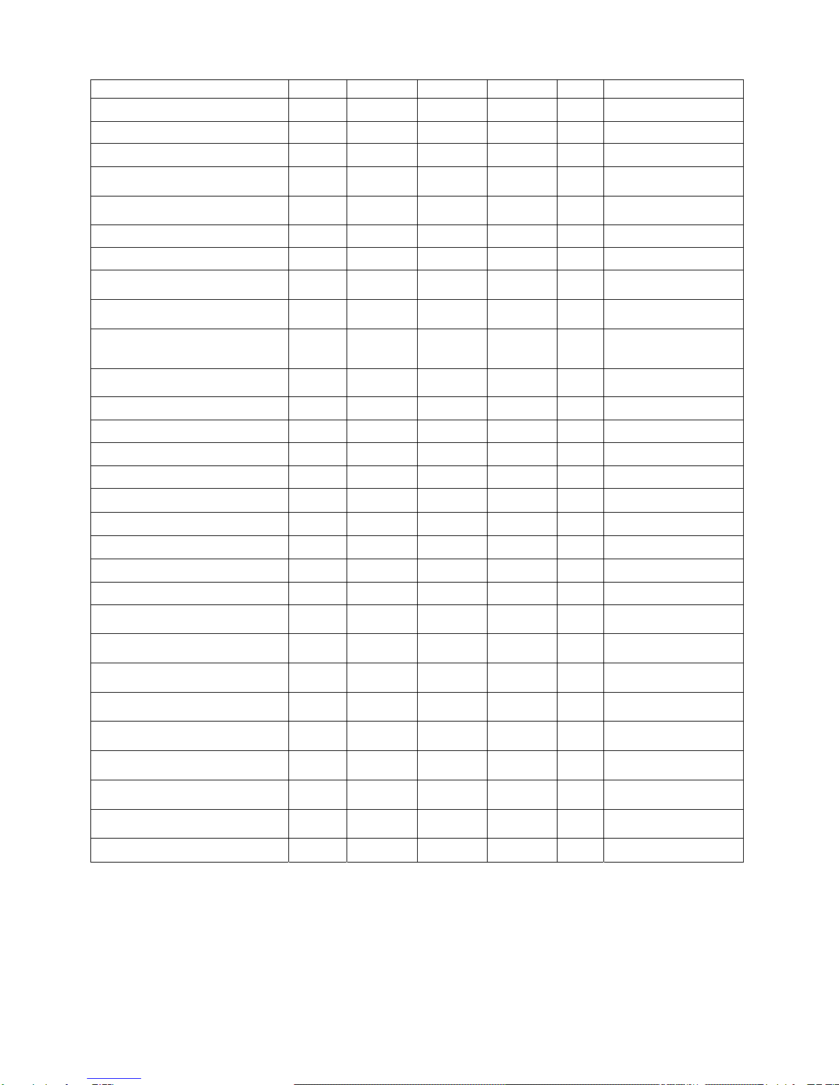
●Electrical Characteristics ( VCC = 3.0V, DVI = 3.0V, Ta = 25℃, unless otherwise noted )
Parameter Symbol Min. Typ. Max. Units Conditions
Supply Current Icc1 -120 190 uA Ev = 100 lx ※1
Powerdown Current Icc2 -0.01 1.0 uA No input Light
Peak Wave Length λp -560 -nm
Measurement Accuracy S/A 1.02 1.2 1.38 times
Sensor out / Actual lx
EV = 1000 lx ※1, ※2
Dark ( 0 lx ) Sensor out S0 0 0 2 count H-Resolution Mode ※3
H-Resolution Mode Resolution rHR -1 -lx
L-Resolution Mode Resolution rLR -4 -lx
H-Resolution Mode Measurement
Time tHR -120 180 ms
L-Resolution Mode Measurement
Time tLR -16 24 ms
Incandescent / Fluorescent Sensor
out ratio rIF -1 -times
EV = 1000 lx
ADDR Input ‘H’ Voltage VAH 0.7 * VCC --V
ADDR Input ‘L’ Voltage VAL --0.3 * VCC V
DVI Input ‘L’ Voltage VDVL --0.4 V
SCL, SDA Input ‘H’ Voltage 1 VIH1 0.7 * DVI --V DVI ≧1.8V
SCL, SDA Input ‘H’ Voltage 2 VIH2 1.26 --V 1.65V ≦DVI <1.8V
SCL, SDA Input ‘L’ Voltage 1 VIL1 --0.3 * DVI V DVI ≧1.8V
SCL, SDA Input ‘L’ Voltage 2 VIL2 --DVI – 1.26 V 1.65V ≦DVI <1.8V
SCL, SDA, ADDR Input ‘H’ Current IIH --10 uA
SCL, SDA, ADDR Input ‘L’ Current IIL --10 uA
I2C SCL Clock Frequency fSCL --400 kHz
I2C Bus Free Time tBUF 1.3 --us
I2C Hold Time ( repeated ) START
Condition tHDSTA 0.6 --us
I2C Set up time for a Repeated
START Condition tSUSTA 0.6 --us
I2C Set up time for a Repeated
STOP Condition tSUSTD 0.6 --us
I2C Data Hold Time tHDDAT 0 -0.9 us
I2C Data Setup Time tSUDAT 100 --ns
I2C ‘L’ Period of the SCL Clock tLOW 1.3 --us
I2C ‘H’ Period of the SCL Clock tHIGH 0.6 --us
I2C SDA Output ‘L’ Voltage VOL 0 -0.4 V IOL = 3 mA
※1White LED is used as optical source.
※2 Measurement Accuracy typical value is possible to change '1' by "Measurement result adjustment function".
※3 Use H-Resolution Mode if dark data ( less than 10 lx ) is need.
Downloaded from Elcodis.com electronic components distributor
3 / 15
●Reference Data
Fig.8 Light Source Dependency
( Fluorescent Light is set to '1' )
1
10
100
1000
10000
100000
1 10 100 1000 10000 100000
Illuminance [ lx ]
Measurement Result
Fig.4 Directional Characteristics 1 Fig.5 Directional Characteristics 2
Fig.6 Dark Response
蛍光灯白熱灯感度比
VCC vs. ICC@測定
中
受信指向角特性
0
0.2
0.4
0.6
0.8
1
1.2
-90 -60 -30 0 30 60 90
Angle [ deg ]
Ratio
0
0.2
0.4
0.6
0.8
1
1.2
-90 -60 -30 0 30 60 90
Angle [ deg ]
Ratio
0
2
4
6
8
10
-40 -10 20 50 80 110
Ta [ ℃]
Measurement Result
0
50
100
150
200
2 2.5 3 3.5 4
VCC [ V ]
ICC @ Measurement
00.511.52
Fluorescent
Light
Incandescent
Light
Halogen
Light
Kripton Light
Artifical Sun
Light
White LED
Ratio
H-Res. L-Res.
0
8
16
24
32
40
48
56
64
0 8 16 24 32 40 48 56 64
Illuminance [ lx ]
Measurement Result
H-Res.
L-Res.
H-Res.
-
+
-
+
-
+
-
+
1pin
1pin
0
0.2
0.4
0.6
0.8
1
1.2
400 500 600 700 800 900 1000 1100
Wavelength [ nm ]
Ratio
Fig.7 Measurement Result
Temperature Dependency
Fig.2 Illuminance –
Measurement Result 1
Fig.3 Illuminance –
Measurement Result 2
Fig.9 VCC – ICC
( During measurement )
Fig.10 VCC – ICC@0 Lx
( POWER DOWN )
Fig.1 Spectral Response
0
0.2
0.4
0.6
0.8
1
1.2
22.533.54
VCC [ V ]
Ratio
Fig.11 Measurement Result
VCC Dependency
0
0.2
0.4
0.6
0.8
1
1.2
1.5 2 2.5 3 3.5
DVI [ V ]
Ratio
Fig.12 Measurement Result
DVI Dependency
DVI=1.8V VCC=3V
0.01
0.1
1
10
-40 -20 0 20 40 60 80
Ta [ ℃]
ICC @ POWER DOWN [ uA ]
0
0.2
0.4
0.6
0.8
1
1.2
-40 -10 20 50 80 110
Ta [ ℃]
Ratio
Downloaded from Elcodis.com electronic components distributor
4 / 15
●Block Diagram
●Block Diagram Descriptions
zPD
Photo diode with approximately human eye response.
zAMP
Integration-OPAMP for converting from PD current to Voltage.
zADC
AD converter for obtainment Digital 16bit data.
zLogic + I2C Interface
Ambient Light Calculation and I2C BUS Interface. It is including below register.
Data Register →This is for registration of Ambient Light Data. Initial Value is "0000_0000_0000_0000".
Measurement Time Register →This is for registration of measurement time. Initial Value is "0100_0101".
zOSC
Internal Oscillator ( typ. 320kHz ). It is CLK for internal logic.
●Measurement Procedure
* "Power On" Command is possible to omit.
SCL
SDA
GND ADDR
PD
VCC DVI
Logic
+
I2C Interface
ADC
AMP
OSC
State Transition by I2C write-command.
Automatically State Transition
State is automatically changed to
Power Down mode.
Power supply
Power Down
Power On
Measurement Command
Initial state is Power Down mode after
VCC and DVI supply.
One Time Measurement Continuous Measurement
Downloaded from Elcodis.com electronic components distributor
5 / 15
●Instruction Set Architecture
Instruction Opecode Comments
Power Down 0000_0000 No active state.
Power On 0000_0001 Waiting for measurement command.
Reset 0000_0111
Reset Data register value. Reset command is not acceptable in
Power Down mode.
Continuously H-Resolution Mode 0001_0000
Start measurement at 1lx resolution.
Measurement Time is typically 120ms.
Continuously L-Resolution Mode 0001_0011
Start measurement at 4lx resolution.
Measurement Time is typically 16ms.
One Time H-Resolution Mode 0010_0000
Start measurement at 1lx resolution.
Measurement Time is typically 120ms.
It is automatically set to Power Down mode after measurement.
One Time L-Resolution Mode 0010_0011
Start measurement at 4lx resolution.
Measurement Time is typically 16ms.
It is automatically set to Power Down mode after measurement.
Change Measurement time
( High bit ) 01000_MT[7,6,5]
Change measurement time.
※Please refer "adjust measurement result for influence of optical
window."
Change Measurement time
( Low bit ) 011_MT[4,3,2,1,0]
Change measurement time.
※Please refer "adjust measurement result for influence of optical
window."
※Don't input the other opecode.
●Measurement mode explanation
Measurement Mode Measurement Time. Resolution
H-Resolution Mode Typ. 120ms. 1 Lx.
L-Resolution Mode Typ. 16ms. 4 Lx.
We recommend to use H-Resolution Mode.
Measurement time ( integration time ) of H-Resolution Mode is so long that some kind of noise( including in 50Hz / 60Hz noise ) is
rejected. And H-Resolution Mode is 1 l x resolution so that it is suitable for darkness ( less than 10 lx )
●Explanation of Asynchronous reset and Reset command "0000_0111"
1) Asynchronous reset
All registers are reset. It is necessary on power supply sequence. Please refer "Timing chart for VCC and DVI power supply
sequence" in this page. It is power down mode during DVI = 'L'.
2) Reset command
Reset command is for only reset Illuminance data register. ( reset value is '0' ) It is not necessary even power supply
sequence. It is used for removing previous measurement result. This command is not working in power down mode, so that
please set the power on mode before input this command.
Downloaded from Elcodis.com electronic components distributor
6 / 15
●Timing chart for VCC and DVI power supply sequence
DVI is I2C bus reference voltage terminal. And it is also asynchronous reset terminal. It is necessary to set to 'L' after VCC
is supplied. In DVI 'L' term, internal state is set to Power Down mode.
1) Recommended Timing chart1 for VCC and DVI supply.
2) Timing chart2 for VCC and DVI supply.
(If DVI rises within 1us after VCC supply )
VCC
DVI
Reset Term ( more than 1us )
VCC
DVI
Don't care state
ADDR, SDA, SCL is not stable if DVI 'L' term ( 1us ) is not given by systems.
In this case, please connect the resisters ( approximately 100kOhm ) to ADDR without directly
connecting to VCC or GND,
Reset Term ( more than 1us )
Downloaded from Elcodis.com electronic components distributor
7 / 15
●Measurement sequence example from "Write instruction" to "Read measurement result"
ex1) Continuously H-resolution mode ( ADDR = 'L' )
①Send "Continuously H-resolution mode " instruction
ST 0100011 0 Ack 00010000 Ack SP
②Wait to complete 1st H-resolution mode measurement.( max. 180ms. )
③Read measurement result.
ST 0100011 1 Ack High Byte [ 15:8 ] Ack
Low Byte [ 7:0 ] Ack SP
How to calculate when the data High Byte is "10000011" and Low Byte is "10010000"
(2
15 + 29 + 28 + 27 + 24) / 1.2 ≒28067 [ lx ]
The result of continuously measurement mode is updated.( 120ms.typ at H-resolution mode, 16ms.typ at L-resolution
mode )
ex2 ) One time L-resolution mode ( ADDR = 'H' )
①Send "One time L-resolution mode " instruction
ST 1011100 0 Ack 00100011 Ack SP
②Wait to complete L-resolution mode measurement.( max. 24ms. )
③Read measurement result
ST 1011100 1 Ack High Byte [ 15:8 ] Ack
Low Byte [ 7:0 ] Ack SP
How to calculate when the data High Byte is "00000001" and Low Byte is "00010000"
(2
8 + 24) / 1.2 ≒227 [ lx ]
In one time measurement, Statement moves to power down mode after measurement completion. If updated result is
need then please resend measurement instruction.
from Master to Slave from Slave to Master
Downloaded from Elcodis.com electronic components distributor
8 / 15
●Application circuit example of DVI terminal
The DVI terminal is an asynchronous reset terminal. Please note that there is a possibility that IC doesn't operate normally if
the reset section is not installed after the start-up of VCC. (Please refer to the paragraph of "Timing chart for VCC and DVI
power supply sequence" )
The description concerning SDA and the terminal SCL is omitted in this application circuit example. Please design the
application the standard of the I2C bus as it finishes being satisfactory. Moreover, the description concerning the terminal
ADDR is omitted. Please refer to the paragraph of "Timing chart for VCC and DVI power supply sequence" about the
terminal ADDR design.
ex 1) The control signal line such as CPU is connected.
ex 2) Reset IC is used.
1, For Reset IC of the Push-Pull type
2, For Reset IC of the Open drain output
ex 3) A different power supply is used.
※Power supply of DVI must stand up later than power supply of VCC stand up, because it is necessary to secure reset section
( 1us or more ).
Micro
Controller
VCC
ADDR
SCL
SDA
0.1uF
0.1uF
DVI
GND
BH1715FVC
VCC
ADDR
SCL
SDA
0.1uF
DVI
GND
RESET
Reset IC( Push-Pull type )
BH1715FVC
0.1uF
VCC
ADDR
SCL
SDA
0.1uF
DVI
GND
Reset IC( Open drain type )
RESET
1kOhm
BH1715FVC
0
.1
u
F
BH1715FVC
VCC
ADDR
SCL
SDA 0.1uF
DVI
GND
0
.1
u
F
V2
V1
Downloaded from Elcodis.com electronic components distributor
9 / 15
ex 4) LPF using CR is inserted between VCC and DVI.
This method has the possibility that the Reset section of turning on the power supply can not satisfied. cannot be satisfied.
Please design the set considering the characteristic of the power supply enough.
Notes when CR is inserted between VCC and DVI
※Please note that there is a possibility that reset section ( 1us ) can not be satisfied because the power supply is turned on
when the rise time of VCC is slow
※When VCC is turned off, the DVI voltage becomes higher than VCC voltage but IC destruction is not occurred if
recommended constant ( R1 = 1kOhm, C1 = 1uF ) is used.
※Please note that there is a possibility that Reset section (1usec) cannot be satisfied if wait time is not enough long after
turning off VCC.(It is necessary to consider DVI voltage level after turning off VCC.)
Example of designing set when CR ( C = 1uF, R = 1kΩ) is inserted between VCC and DVI with VCC=2.8V
① The rise time to 0→2.4V of VCC must use the power supply of 100us or less.
② Please wait 25ms or more after VCC turn off ( VCC <= 0.05V ), because it is necessary to secure reset section ( 1us or more ).
R1 : 1kOhm
0.1uF C1 : 1uF
VCC
ADDR
GND
SCL
DVI
SDA
BH1715FVC
Reset Section : 1us or more
t1 VCC
DVI
2.4V
0.4V
0V
* Please do the application design to secure Reset section 1us or more after the reclosing of the power supply.
Reset Section : 1us or more
Rise time of
p
ower su
pp
l
y
: 100us or less
0.05V
Time to power supply reclosing : 25ms or more VCC
DVI
2.4V
0.4V
2.8V
0V
t2
* Please do the application design to secure Reset section 1us or more after the reclosing of the power supply.
Downloaded from Elcodis.com electronic components distributor
10 / 15
●I
2C Bus Access
1 ) I2C Bus Interface Timing chart
Write measurement command and Read measurement result are done by I2C Bus interface. Please refer the formally
specification of I2C Bus interface, and follow the formally timing chart.
2) Slave Address
Slave Address is 2 types, it is determined by ADDR Terminal
ADDR = ‘H’ ( ADDR ≧0.7VCC ) → “1011100“
ADDR = 'L' ( ADDR ≦0.3VCC ) → “0100011“
3 ) Write Format
BH1715FVC is not able to accept plural command without stop condition. Please insert SP every 1 Opecode.
ST Slave Address R/W
0 Ack Opecode Ack SP
4 ) Read Format
ST Slave Address R/W
1 Ack High Byte [15:8]
215 214 213 212 211 210 29 28Ack
Low Byte [7:0]
27 26 25 24 23 22 21 20Ack SP
ex )
High Byte = "1000_0011"
Low Byte = "1001_0000"
( 215 + 29 + 28 + 27 + 24 ) / 1.2 ≒ 28067 [ lx ] ※2
* I2C BUS is trademark of Phillips Semiconductors. Please refer formality specification.
from Master to Slave from Slave to Master
tHD ; DAT
S
SDA
SCL
S
tHD ; STA
tLOW
tftr
Sr
tSU ; STA
tSU
;
DAT tf
tSU;STO
tBUF
S
P
tr
S
tHIGH
tHD ; STA
Downloaded from Elcodis.com electronic components distributor
11 / 15
●Adjust measurement result for influence of optical window.
BH1715FVC is including in adjust measurement result function for influence of optical window. Adjust is done by changing
measurement time. For example, if transmission rate by optical window is 1 / N, then adjust is done by measurement time is
set to "initial value * N".
Measurement time register ( Mtreg ) is 8bit register. Initial value is "0100_0101" ( 45xh ). Please change this register value
via to I2C Bus interface.
ex ) Case of transmission rate is 50%.
Please change Mtreg value from "0100_0101" to "1000_1010".
1) Changing High bit of Mtreg
ST Slave Address R/W
0 Ack 01000_100 Ack SP
2) Changing Low bit of Mtreg
ST Slave Address R/W
0 Ack 011_01010 Ack SP
3) Input Measurement Command.
ST Slave Address R/W
0 Ack 0001_0000 Ack SP
※ This example is High Resolution mode, but it accepts the other measurement.
4) After about 240ms, measurement result is registered to Data Register. ( High Resolution mode is typically 120ms, but
measurement time is set twice. )
Supported Mtreg value is seeing below.
Min. Typ. Max
Supported value ( hex ) 0010_1101
( transmission rate 153% )
0100_0101
( transmission rate 100% )
1111_1110
( transmission rate 27.2% )
For example BH1715FVC is possible to detect min. 0.33 lx when Mtreg value is “1111_1110” at H-Resolution mode.
Downloaded from Elcodis.com electronic components distributor
12 / 15
●Terminal Description
PIN
No.
Terminal Name Equivalent Circuit Function
1 VCC
Power Supply Terminal
2 ADDR
I2C Slave-address Terminal
ADDR = ‘H’ ( ADDR ≧0.7VCC )
“1011100“
ADDR = 'L' ( ADDR ≦0.3VCC )
“0100011“
ADDR Terminal is designed as 3 state buffer
for internal test. So that please take care of
VCC and DVI supply procedure.Please see P6.
3 GND
GND Terminal
4 SDA
I2C bus Interface SDA Terminal
5 DVI
SDA, SCL Reference Voltage Terminal
And DVI Terminal is also asynchronous Reset
for internal registers.So that please set to 'L'
( at least 1us, DVI <= 0.4V ) after VCC is
supplied. BH1715FVC is pulled down by
150kOhm while DVI = 'L'.
6 SCL
I2C bus Interface SCL Terminal
※ These values are design-value, not guaranteed.
150kOhm
VCC
Downloaded from Elcodis.com electronic components distributor
13 / 15
●Package Outlines
●About an optical design on the device
0.8 mm
1.3 mm
PD area ( 0.25 mm x 0.3 mm )
Please design the optical window so that
light can cover at least this area.
Min.0.4 mm
Min.0.4 mm
Min.0.4 mm
Min.0.4 mm
WSOF6 ( Unit : mm )
A
D
Lot No.
Production
code
Downloaded from Elcodis.com electronic components distributor
14 / 15
●Cautions on use
1) Absolute Maximum Ratings
An excess in the absolute maximum ratings, such as supply voltage ( Vmax ), temperature range of operating
conditions ( Topr ), etc., can break down devices, thus making impossible to identify breaking mode such as a short
circuit or an open circuit. If any special mode exceeding the absolute maximum ratings is assumed, consideration
should be given to take physical safety measures including the use of fuses, etc.
2) GND voltage
Make setting of the potential of the GND terminal so that it will be maintained at the minimum in any operating state.
Furthermore, check to be sure no terminals are at a potential lower than the GND voltage including an actual
electric transient.
3) Short circuit between terminals and erroneous mounting
In order to mount ICs on a set PCB, pay thorough attention to the direction and offset of the ICs. Erroneous
mounting can break down the ICs. Furthermore, if a short circuit occurs due to foreign matters entering between
terminals or between the terminal and the power supply or the GND terminal, the ICs can break down.
4) Operation in strong electromagnetic field
Be noted that using ICs in the strong electromagnetic field can malfunction them.
5) Inspection with set PCB
On the inspection with the set PCB, if a capacitor is connected to a low-impedance IC terminal, the IC can suffer
stress. Therefore, be sure to discharge from the set PCB by each process. Furthermore, in order to mount or
dismount the set PCB to/from the jig for the inspection process, be sure to turn OFF the power supply and then
mount the set PCB to the jig. After the completion of the inspection, be sure to turn OFF the power supply and then
dismount it from the jig. In addition, for protection against static electricity, establish a ground for the assembly
process and pay thorough attention to the transportation and the storage of the set PCB.
6) Input terminals
In terms of the construction of IC, parasitic elements are inevitably formed in relation to potential. The operation of
the parasitic element can cause interference with circuit operation, thus resulting in a malfunction and then
breakdown of the input terminal. Therefore, pay thorough attention not to handle the input terminals; such as to
apply to the input terminals a voltage lower than the GND respectively, so that any parasitic element will operate.
Furthermore, do not apply a voltage to the input terminals when no power supply voltage is applied to the IC. In
addition, even if the power supply voltage is applied, apply to the input terminals a voltage lower than the power
supply voltage or within the guaranteed value of electrical characteristics.
7) Thermal design
Perform thermal design in which there are adequate margins by taking into account the power dissipation ( Pd ) in
actual states of use.
8) Treatment of package
Dusts or scratch on the photo detector may affect the optical characteristics. Please handle it with care.
9) Rush current
When power is first supplied to the CMOS IC, it is possible that the internal logic may be unstable and rush current
may flow instantaneously. Therefore, give special consideration to power coupling capacitance, power wiring, width
of GND wiring, and routing of connections.
10) The exposed central pad on the back side of the package
There is an exposed central pad on the back side of the package. But please do it non connection. ( Don't solder,
and don't do electrical connection ) Please mount by Footprint dimensions described in the Jisso Information for
WSOF6. This pad is GND level, therefore there is a possibility that LSI malfunctions and heavy-current is
generated.
Downloaded from Elcodis.com electronic components distributor
15 / 15
●Product Designations (Selecting a model name when ordering)
RohmModel Part number Package type TR = Reel-wound embossed taping
B H 1 7 1 5
-
T RF V C
WSOF6
(Unit:mm)
<Dimension>
Tape
Quantity
Direction
of feed
Embossed carrier tape
3000pcs
(The direction is the 1pin of product is at the upper right when you hold
reel on the left hand and you pull out the tape on the right hand)
<Tape and Reel information>
TR
※When you order , please order in times the amount of package quantity.
Direction of feed
1Pin
XXX
XXX
XXX
XXX
XXX
XXX
X X X
XXXX X X
XXX
Catalog No.08T164A '08.6 ROHM © 1000 NZ
Downloaded from Elcodis.com electronic components distributor
Notes
No technical content pages of this document may be reproduced in any form or transmitted by any
means without prior permission of ROHM CO.,LTD.
The contents described herein are subject to change without notice. The specifications for the
product described in this document are for reference only. Upon actual use, therefore, please request
that specifications to be separately delivered.
Application circuit diagrams and circuit constants contained herein are shown as examples of standard
use and operation. Please pay careful attention to the peripheral conditions when designing circuits
and deciding upon circuit constants in the set.
Any data, including, but not limited to application circuit diagrams information, described herein
are intended only as illustrations of such devices and not as the specifications for such devices. ROHM
CO.,LTD. disclaims any warranty that any use of such devices shall be free from infringement of any
third party's intellectual property rights or other proprietary rights, and further, assumes no liability of
whatsoever nature in the event of any such infringement, or arising from or connected with or related
to the use of such devices.
Upon the sale of any such devices, other than for buyer's right to use such devices itself, resell or
otherwise dispose of the same, no express or implied right or license to practice or commercially
exploit any intellectual property rights or other proprietary rights owned or controlled by
ROHM CO., LTD. is granted to any such buyer.
Products listed in this document are no antiradiation design.
Appendix1-Rev2.0
Thank you for your accessing to ROHM product informations.
More detail product informations and catalogs are available, please contact your nearest sales office.
ROHM Customer Support System THE AMERICAS /EUROPE /ASIA /JAPAN
Contact us : webmaster@ rohm.co.jp
www.rohm.com
Copyright © 2008 ROHM CO.,LTD.
The products listed in this document are designed to be used with ordinary electronic equipment or devices
(such as audio visual equipment, office-automation equipment, communications devices, electrical
appliances and electronic toys).
Should you intend to use these products with equipment or devices which require an extremely high level
of reliability and the malfunction of which would directly endanger human life (such as medical
instruments, transportation equipment, aerospace machinery, nuclear-reactor controllers, fuel controllers
and other safety devices), please be sure to consult with our sales representative in advance.
It is our top priority to supply products with the utmost quality and reliability. However, there is always a chance
of failure due to unexpected factors. Therefore, please take into account the derating characteristics and allow
for sufficient safety features, such as extra margin, anti-flammability, and fail-safe measures when designing in
order to prevent possible accidents that may result in bodily harm or fire caused by component failure. ROHM
cannot be held responsible for any damages arising from the use of the products under conditions out of the
range of the specifications or due to non-compliance with the NOTES specified in this catalog.
21 Saiin Mizosaki-cho, Ukyo-ku, Kyoto 615-8585, Japan TEL : +81-75-311-2121
FAX : +81-75-315-0172
Appendix
Downloaded from Elcodis.com electronic components distributor

This manual suits for next models

1

Other Rohm Accessories manuals

Rohm BH1730FVC Instruction Manual

Rohm

Rohm BH1730FVC Instruction Manual

Rohm RPR-0521RS-EVK-001 User manual

Rohm

Rohm RPR-0521RS-EVK-001 User manual

Rohm SENSEKIT1-EVK-101-ND User manual

Rohm

Rohm SENSEKIT1-EVK-101-ND User manual

Popular Accessories manuals by other brands

Yamaha HY144-D Firmware update guide

Yamaha

Yamaha HY144-D Firmware update guide

The Siemon Company S210 instructions

The Siemon Company

The Siemon Company S210 instructions

HELVAR 32 TR Series installation guide

HELVAR

HELVAR 32 TR Series installation guide

Altinex SIGNAL MANAGEMENT SOLUTIONS Tilt ‘N Plug... user guide

Altinex

Altinex SIGNAL MANAGEMENT SOLUTIONS Tilt ‘N Plug... user guide

Emos P5521N instructions

Emos

Emos P5521N instructions

Mohlenhoff WLK 180 manual

Mohlenhoff

Mohlenhoff WLK 180 manual

Saxby 54414 Instruction leaflet

Saxby

Saxby 54414 Instruction leaflet

Siemens SITRANS WS300 operating instructions

Siemens

Siemens SITRANS WS300 operating instructions

IFM PI17 Series operating instructions

IFM

IFM PI17 Series operating instructions

LaserPoint AHA-5-D12 instruction manual

LaserPoint

LaserPoint AHA-5-D12 instruction manual

IFM Electronic LK7 operating instructions

IFM Electronic

IFM Electronic LK7 operating instructions

Gardena 19030 Operator's manual

Gardena

Gardena 19030 Operator's manual

Huawei Airbridge BTS3612A Technical manual

Huawei

Huawei Airbridge BTS3612A Technical manual

Hiltron SA quick start guide

Hiltron

Hiltron SA quick start guide

Defy DFD 211 instruction manual

Defy

Defy DFD 211 instruction manual

Grizzly H8368 instructions

Grizzly

Grizzly H8368 instructions

Carefree of Colorado SOKIII Service manual

Carefree of Colorado

Carefree of Colorado SOKIII Service manual

IFM Electronic Efector160 LK3 operating instructions

IFM Electronic

IFM Electronic Efector160 LK3 operating instructions

manuals.online logo
manuals.online logoBrands
  • About & Mission
  • Contact us
  • Privacy Policy
  • Terms and Conditions

Copyright 2025 Manuals.Online. All Rights Reserved.