Technical Note
2/20
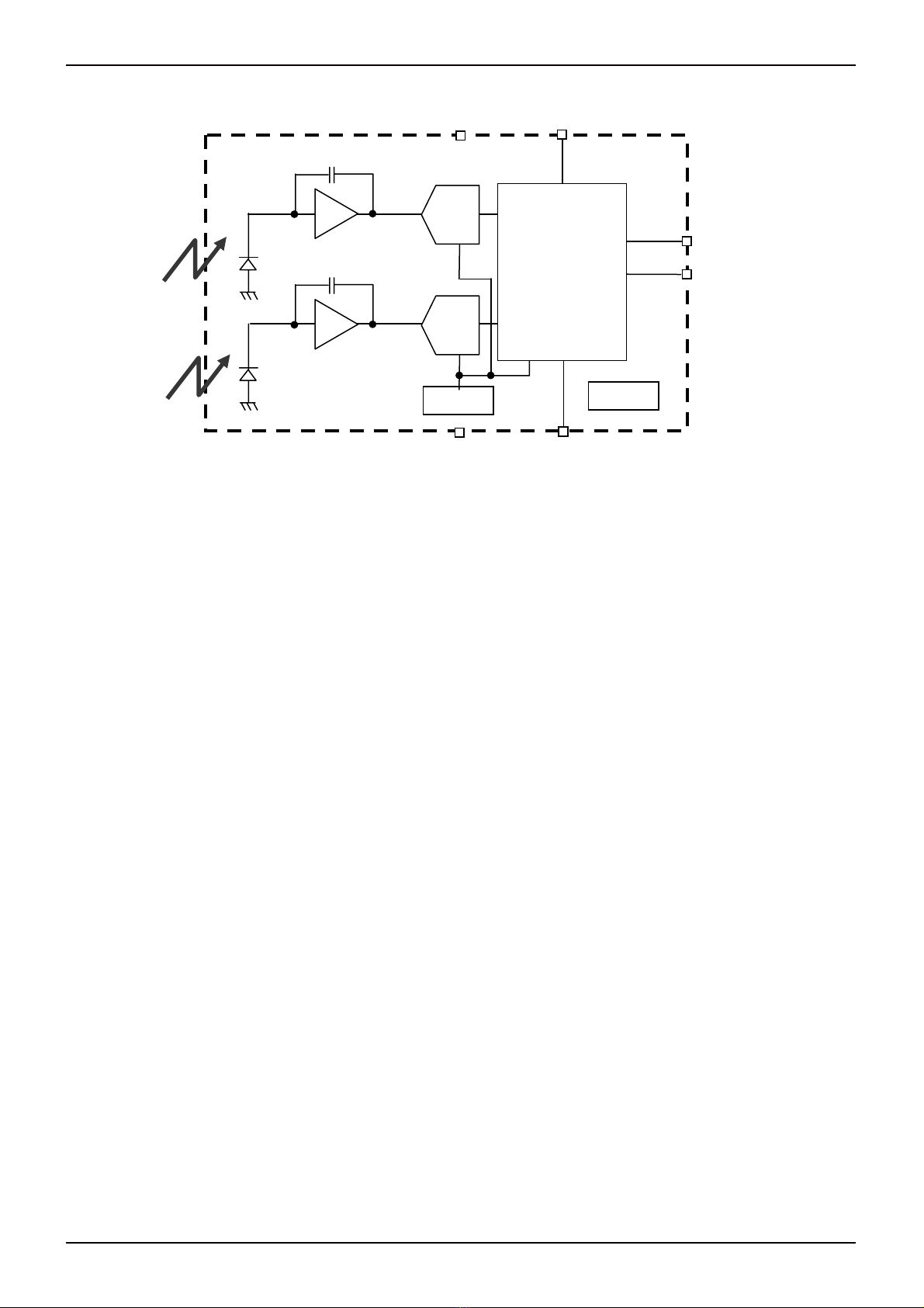
BH1730FVC
www.rohm.com 2012.02 - Rev.A
© 2012 ROHM Co., Ltd. All rights reserved.
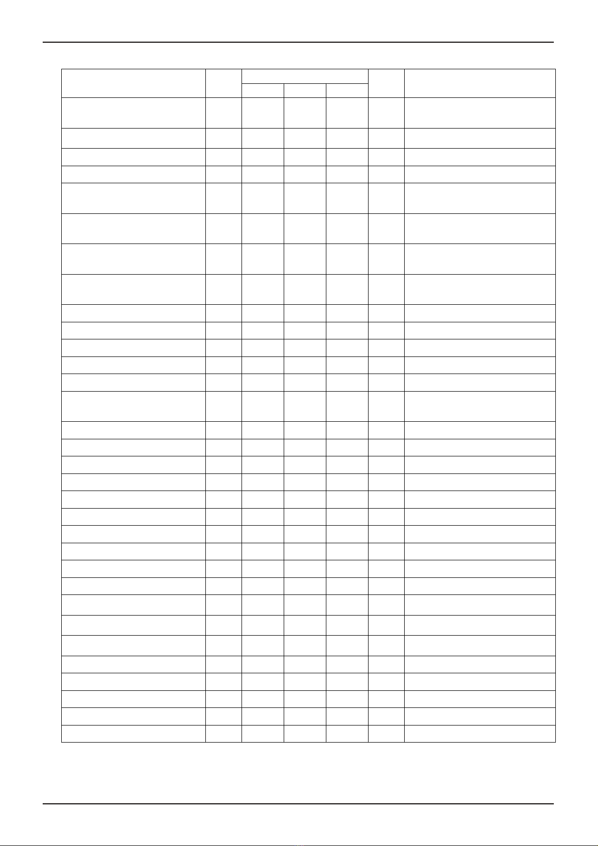
●Electrical Characteristics ( VCC = 3.0V, VDVI = 3.0V, Ta = 25℃, unless otherwise noted )
Parameter Symbol Limits Units Conditions
Min. Typ. Max.
Supply Current Icc1 -150 200 uA
Ev = 100 lx ※
CONTROL register(00h) = ”03h”
and the other registers are default.
Powerdown Current Icc2 -0.85 1.5 uA
No input Light
All registers are default.
Peak Wave Length in Type0 λp0 -600 -nm Visible light response
Peak Wave Length in Type1 λp1 -840 -nm Infrared light response
ADC count value in Type0 D1k_0 1020 1200 1380 count
EV = 1000 lx ※
TIMING register(01h) = “DAh”
GAIN register(07h) = “00h”
ADC count value in Type1 D1k_1 153 180 207 count
EV = 1000 lx ※
TIMING register(01h) = “DAh”
GAIN register(07h) = “00h”
Dark ( 0 lx ) Sensor out in Type0 S0_0 0 0 2 count
No input Light
TIMING register(01h) = “DAh”
GAIN register(07h) = “00h”
Dark ( 0 lx ) Sensor out in Type1 S0_1 0 0 2 count
No input Light
TIMING register(01h) = “DAh”
GAIN register(07h) = “00h”
Gain X1 resolution in Type0 rG1 -0.83 -lx/count TIMING register(01h) = “DAh” ※1
Gain X2 resolution in Type0 rG2 -0.42 -lx/count TIMING register(01h) = “DAh” ※1
Gain X64 resolution in Type0 rG64 -0.014 -lx/count TIMING register(01h) = “DAh” ※1
Gain X128 resolution in Type0 rG128 -0.007 -lx/count TIMING register(01h) = “DAh” ※1
Measurement Time tmt1 -100 150 ms TIMING register(01h) = “DAh”
Incandescent / Fluorescent ratio
by calculating with Type0 and
Type1
rIF -1 -times EV = 1000 lx
INT Output ‘L’ Voltage VINT 0 -0.4 V IINT = 3 mA
DVI Input ‘L’ Voltage VDVL --0.4 V
SCL, SDA Input ‘H’ Voltage 1 VIH1 0.7*DVI --V DVI ≧1.8V
SCL, SDA Input ‘H’ Voltage 2 VIH2 1.26 --V 1.65V ≦DVI <1.8V
SCL, SDA Input ‘L’ Voltage 1 VIL1 --0.3*DVI V DVI ≧1.8V
SCL, SDA Input ‘L’ Voltage 2 VIL2 --DVI–1.26 V 1.65V ≦DVI <1.8V
SCL, SDA, INT Input ‘H’ Current IIH --10 µA
SCL, SDA, INT Input ‘L’ Current IIL --10 µA
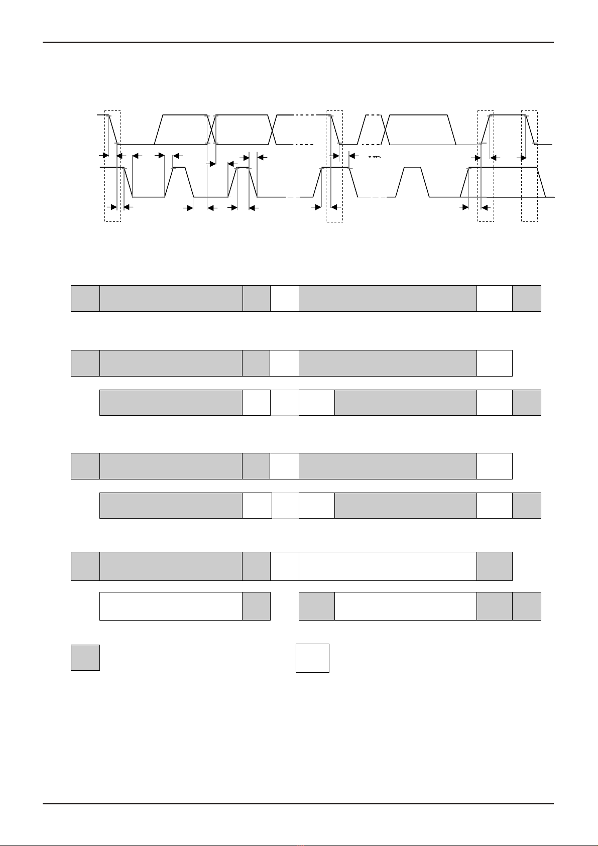
I2C SCL Clock Frequency fSCL --400 kHz
I2C Bus Free Time tBUF 1.3 --µs
I
C Hold Time ( repeated ) START
Condition tHDSTA 0.6 --µs
I
C Set up time for a Repeated
START Condition tSUSTA 0.6 --µs
I
C Set up time for STOP
Condition tSUSTO 0.6 --µs
I2C Data Hold Time tHDDAT 0 -0.9 µs
I2C Data Setup Time tSUDAT 100 --ns
I2C ‘L’ Period of the SCL Clock tLOW 1.3 --µs
I2C ‘H’ Period of the SCL Clock tHIGH 0.6 --µs
I2C SDA Output ‘L’ Voltage VOL 0 -0.4 V IOL = 3 mA
※1 White LED is used as optical source.