manuals.online logo
Brands
  1. Home
  2. •
  3. Brands
  4. •
  5. Rohm
  6. •
  7. Motherboard
  8. •
  9. Rohm BD7F205EFJ-C User manual

Rohm BD7F205EFJ-C User manual

1/25
© 2022 ROHM Co., Ltd.
65UG028E Rev.001
2022.7
User's Guide
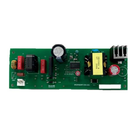
Figure 1. BD7F205EFJ-EVK-001
Isolated DC/DC Converters ICs
Built-in Automotive Switching MOSFET
Isolated Flyback Converter ICs
BD7F205EFJ-C Evaluation Board
BD7F205EFJ-EVK-001
Overview
This evaluation board outputs an isolated 6.2 V, 16.5 V and 6.2 V voltage from an input of 8 V to 32 V, and can output a maximum
output power 6 W.
BD7F205EFJ-C is an isolated flyback converter that does not require a photocoupler.
Feedback circuit by the transformer’s tertiary winding or photocouplers becomes unnecessary, contributing to reduction of set
parts.
It also has a number of built-in protection functions that enable the design of isolated power supply applications for high reliability.
2/25
© 2022 ROHM Co., Ltd.
65UG028E Rev.001
2022.7
User's Guide
Performance Specifications
This is a typical value and does not guarantee the characteristics.
Unless otherwise specified, VIN = 12 V, IOUT = 0.1 A, Ta = 25 °C
Parameter
Symbol
Min
Typ
Max
Units
Conditions
Input voltage range
VIN
8
12
32
V
Output voltage 1
VOUT1
5.5
6.2
6.9
V
IOUT1 = 0.1 A
Output voltage 2
VOUT2
14.8
16.5
18.2
V
IOUT2 = 0.1 A
Output voltage 3
VOUT3
5.5
6.2
6.9
V
IOUT3 = 0.1 A
Output current 1
IOUT1
0
0.3
A
Output current 2
IOUT2
0
0.1
A
Output current 3
IOUT3
0
0.3
A
Maximum output power
POUT
-
-
6
W
Standby power
PINSTBY
-
40
100
mW
IOUT = 0 A VIN = 12 V
Power Supply Efficiency
η
60
75
-
%
POUT = 2 W
3/25
© 2022 ROHM Co., Ltd.
65UG028E Rev.001
2022.7
User's Guide
BD7F105EFJ-EVK-001
Figure 2. Connection Diagram
Operating Procedure
1. Necessary equipment
(1) DC power supply of V to 32 V, 10 W / 5 A or more
(2) Load device up to 5 W
(3) DC voltmeter
2. Connecting the Equipment
(1) Preset the DC power supply to 8 V to 32 V and turn off the power output.
(2) Set the load to less than or equal to the rated current of each output and disable the load.
(3) Connect the positive terminal of the power supply to the VIN terminal and the negative terminal to the GND
terminal with a pair of wires.
(4) Connect the positive terminal of the load to VOUT terminal and the negative terminal to GND terminal with a
pair of wires.
(5) When connecting a wattmeter, connect as shown below. (Refer to your power meter User's Manual for more
information)
(6) Connect the positive terminal of the DC voltmeter to VOUT terminal and the negative terminal to GND terminal
for measuring the output voltage.
(7) Turn on the output of the DC power supply.
(8) Check that the DC voltmeter display is at the set voltage.
(9) Activates the load.
4/25
© 2022 ROHM Co., Ltd.
65UG028E Rev.001
2022.7
User's Guide
BD7F105EFJ-EVK-001
Figure 3. Circuit diagram
Application circuit
The evaluation board operates with an average frequency of approximately 363 kHz.
Monitoring the flyback voltage due to the voltage at the output provides primary-side feedback control that eliminates the
need for photocouplers and auxiliary windings.
Operation starts when the VIN pin voltage exceeds UVLO detect voltage of 3.4 V (Typ) and SDXEN pin Enable pin voltage of
2.0 V (Typ).
The circuit diagram of the demonstration board is shown in the figure below, and the parts list is shown on page 12.
5/25
© 2022 ROHM Co., Ltd.
65UG028E Rev.001
2022.7
User's Guide
BD7F105EFJ-EVK-001
1
2
3
4
8
7
6
5
GND
SDX/EN
L_COMP
REF
VIN
SW
N.C.
FB
EXP-PAD
(TOP VIEW)
Figure 4. Pin layout drawing
Outline of BD7F205EFJ-C
Features
◼AEC-Q100 (Grade-1)
◼No Need for Optocoupler and Third Winding of
Transformer
◼Output voltage is set by two external resistors and
transformer winding ratio.
◼Uses proprietary adaptive ON-time control
technology
◼Highly efficient light load mode (PFM operation)
◼Shutdown and Enable control
◼Burst voltage design possible
◼60 V Built-in-switching MOSFET
◼Spread frequency spectrum
◼Soft start function
◼Load current compensation function
◼Various protection functions
Undervoltage protection (UVLO)
Overcurrent protection (OCP)
Overheat protection (TSD)
REF pin open protection (REFOPEN)
Short-circuit protection (SCP)
Battery short-circuit protection (BSP)
Critical Characteristics
◼Input voltage range :
VIN terminal 3.4 V to 42.0 V
SW pin to 60 V
◼Switching frequency : 363 kHz (Typ)
◼Reference voltage accuracy: ±2.8 % (Typ)
◼Shutdown current 0 μA (Typ)
◼Operating temperature range -40 °C to +125 °C
Package W (Typ) x D (Typ) x H (Max)
HTSOP-J8 4.9 mm x 6.0 mm x 1.0 mm
Applications
Insulated power supply for automotive use (E-Comp, Inverter
etc)
Insulated power supply for industrial equipment
Pin Layout
PIN ASSIGNMENT
No.
Pin name
Function
1
GND
GND terminal
2
SDX/EN
Shutdown/Enable control pin
3
L_COMP
Load current compensation value setting pin
4
REF
Output voltage setting pin
5
FB
Output voltage setting pin
6
N.C.
No Connect
7
SW
Switching output pin
8
VIN
Power input terminal
-
EXP-PAD
Rear heat dissipation pin
6/25
© 2022 ROHM Co., Ltd.
65UG028E Rev.001
2022.7
User's Guide
BD7F105EFJ-EVK-001
Figure 5. Output Voltage1 vs Output Current1
IOUT2=30mA, IOUT3=50mA
Figure 6. Output Voltage2 vs Output Current1
IOUT2=30mA, IOUT3=50mA
Figure 7. Output Voltage3 vs Output Current1
IOUT2=30mA, IOUT3=50mA
Figure 8. Efficiency vs Output Current1
IOUT2=30mA, IOUT3=50mA
Measurement data
1. Load regulation
5.2
5.6
6.0
6.4
6.8
7.2
7.6
0 0.1 0.2 0.3
VOUT3[V]
IOUT1[A]
VIN=8V
VIN=12V
VIN=18V
VIN=32V
50.0
55.0
60.0
65.0
70.0
75.0
80.0
85.0
90.0
0 0.1 0.2 0.3
Efficiency[%]
IOUT[A]
VIN=8V
VIN=12V
VIN=18V
VIN=32V
7/25
© 2022 ROHM Co., Ltd.
65UG028E Rev.001
2022.7
User's Guide
BD7F105EFJ-EVK-001
Figure 9. Output Voltage1 vs Output Current1
IOUT2=100mA, IOUT3=300mA
Figure 10. Output Voltage2 vs Output Current1
IOUT2=100mA, IOUT3=300mA
Figure 11. Output Voltage3 vs Output Current1
IOUT2=100mA, IOUT3=300mA
Figure 12. Efficiency vs Output Current1
IOUT2=100mA, IOUT3=300mA
Measured data-continued
5.2
5.6
6.0
6.4
6.8
7.2
7.6
0 0.1 0.2 0.3
VOUT1[V]
IOUT1[A]
VIN=8V
VIN=12V
VIN=18V
VIN=32V
15.0
15.5
16.0
16.5
17.0
17.5
18.0
18.5
19.0
0 0.1 0.2 0.3
VOUT2[V]
IOUT1[A]
VIN=8V
VIN=12V
VIN=18V
VIN=32V
5.2
5.6
6.0
6.4
6.8
7.2
7.6
0 0.1 0.2 0.3
VOUT3[V]
IOUT1[A]
VIN=8V
VIN=12V
VIN=18V
VIN=32V
50.0
55.0
60.0
65.0
70.0
75.0
80.0
85.0
90.0
0 0.1 0.2 0.3
Efficiency[%]
IOUT[A]
VIN=8V
VIN=12V
VIN=18V
VIN=32V
8/25
© 2022 ROHM Co., Ltd.
65UG028E Rev.001
2022.7
User's Guide
BD7F105EFJ-EVK-001
Figure 13. Output Voltage1 vs Input Voltage
IOUT1=100mA, IOUT2=100mA, IOUT3=300mA
Figure 14. Output Voltage2 vs Input Voltage
IOUT1=100mA, IOUT2=100mA, IOUT3=300mA
Figure 15. Output Voltage3 vs Input Voltage
IOUT1=100mA, IOUT2=100mA, IOUT3=300mA
Figure 16. Frequency vs Input Voltage
IOUT1=100mA, IOUT2=100mA, IOUT3=300mA
Measured data-continued
2. Line regulation
5.2
5.6
6.0
6.4
6.8
7.2
7.6
010 20 30 40
VOUT1[V]
VIN[V]
VOUT1
15.0
15.4
15.8
16.2
16.6
17.0
17.4
17.8
18.2
18.6
19.0
010 20 30 40
VOUT2[V]
VIN[V]
VOUT2
5.2
5.6
6.0
6.4
6.8
7.2
7.6
010 20 30 40
VOUT3[V]
VIN[V]
VOUT3
300
310
320
330
340
350
360
370
380
390
400
010 20 30 40
VOUT3[V]
VIN[V]
Freq
9/25
© 2022 ROHM Co., Ltd.
65UG028E Rev.001
2022.7
User's Guide
BD7F105EFJ-EVK-001
Figure 17. MOSFET Waveform
Vin = 12 V, IOUT1,3 = 0.1 A, IOUT2 = 0.05 A
Figure 18. MOSFET Waveform
Vin = 12 V, IOUT1,3 = 0.3 A, IOUT2 = 0.1 A
Figure 21. Output voltage ripple Waveform
VIN = 12 V / IO1,2,3=0.1, 0.05, 0.1 A
Figure 22. Output voltage ripple Waveform
VIN = 12 V / IO1,2,3=0.3, 0.1, 0.3 A
Measured data-continued
3. Switching waveform
4. Load response waveform
5. Output ripple voltage waveform
VSW (20V/div)
VOUT1 (10V/div)
VSW (20V/div)
VOUT1 (10V/div)
VOUT2 (10V/div)
VOUT3 (10V/div)
VOUT2 (10V/div)
VOUT3 (10V/div)
VSW (20V/div)
VSW (20V/div)
VOUT1 (1Vac/div)
VOUT2 (1Vac/div)
VOUT3 (1Vac/div)
IOUT1 (200mA/div)
Figure 19. Load response
Vin = 12 V, IOUT2 = 0.05 A, IOUT3 = 0.1 A
IOUT1 = 30 mA to 300 mA
VOUT2 (1Vac/div)
VOUT1 (1Vac/div)
VOUT3 (1Vac/div)
IOUT2 (200mA/div)
Figure 20. Load response
Vin = 12 V, IOUT1 = 0.1 A, IOUT3 = 0.1 A
IOUT2 = 10 mA to 100 mA
VOUT1 (50mVac/div)
VOUT2 (50mVac/div)
VOUT3 (50mVac/div)
VOUT1 (50mVac/div)
VOUT2 (50mVac/div)
VOUT3 (50mVac/div)
*This ripple is due to spread spectrum.
10/25
© 2022 ROHM Co., Ltd.
65UG028E Rev.001
2022.7
User's Guide
BD7F105EFJ-EVK-001
Figure 23. Start Up Waveform
Figure 24. Shut Down Waveform
Figure 25. VOUT Short Waveform
Vin = 8 V
Figure 26. VOUT Short Waveform (ZOOM)
Vin = 8 V
Figure 27. VOUT Short Waveform
Vin = 15 V
Figure 28. VOUT Short Waveform (ZOOM)
Vin = 15 V
Measured data-continued
6. Startup/stop waveform
7. Output short waveform
VSW (20V/div)
VSW (20V/div)
VOUT1 (10V/div)
VSW (20V/div)
VOUT1 (10V/div)
VIN (5V/div)
VIN (5V/div)
VIN (10V/div)
VSW (20V/div)
ISW (2A/div)
VOUT (20V/div)
VSW (20V/div)
VIN (10V/div)
ISW (2A/div)
10ms/div
500us/div
VIN (10V/div)
VSW (20V/div)
ISW (2A/div)
ISW (2A/div)
VSW (20V/div)
VIN (10V/div)
10ms/div
500us/div
VOUT2 (10V/div)
VOUT3 (10V/div)
VOUT3 (10V/div)
VOUT2 (10V/div)
VIN (10V/div)
VSW (20V/div)
ISW (2A/div)
11/25
© 2022 ROHM Co., Ltd.
65UG028E Rev.001
2022.7
User's Guide
BD7F105EFJ-EVK-001
Figure 29. Surface Temperature
Vin = 8 V, IOUT1 = 0.3 A, IOUT2 = 0.1 A
IOUT3 = 0.3 A (Ta = 25℃)
Figure 30. Surface Temperature Reference
Figure 31. Peak Current Waveform
Vin = 8 V, IOUT1 = 0.3 A, IOUT2 = 0.1 A
IOUT3 = 0.3 A
Table 1. Tj Calculation
Measured data-continued
Component surface temperature
Tj calculation of IC is calculated using the above table.
Loss of IC is divided into 1: Turn on loss, 2: conduction loss, 3: Turn off loss, and 4: ICC.
Calculate the loss according to Table1 from the actual current waveform and power supply spec.
In this case, Tj is estimated to be 39 °C because Tc = 30.3 °C and ΔTj = 7.41 °C.
Tj should be designed to be 150 °C or less.
In this case, when Ta = 125 °C, Tj = 146 °C, and Tj = 150 °C is not reached, so it can be judged that there is no problem in the
whole temperature range.
VIN (10V/div)
VSW (20V/div)
ISW (2A/div)
VOUT (20V/div)
39℃
VIN (10V/div)
VSW (10V/div)
IOUT (500mA/div)
①
②
③
12/25
© 2022 ROHM Co., Ltd.
65UG028E Rev.001
2022.7
User's Guide
BD7F105EFJ-EVK-001
Figure 32. BD7F205EFJ-EVK-001 Schematic
Circuit diagrams
(Condition) VIN = 8 V to 32 V, VOUT = 16.5 V, 0.2 A
Bill of Materials
*Parts are subject to change without notice.
13/25
© 2022 ROHM Co., Ltd.
65UG028E Rev.001
2022.7
User's Guide
BD7F105EFJ-EVK-001
Transformer specifications
Manufacturer : Sumida Electric Co., Ltd.
https://job.mynavi.jp/conts/n/sp/23/54430_23sumida/
Product name: CEFD2010-00399-T381R
◼External Dimensions
◼Recommended Land
■Terminal connection diagram
14/25
© 2022 ROHM Co., Ltd.
65UG028E Rev.001
2022.7
User's Guide
BD7F105EFJ-EVK-001
Transformer Specifications-continued
■Winding wire and linear/linear type
■ELECTRICAL CHARACTERISTICS
15/25
© 2022 ROHM Co., Ltd.
65UG028E Rev.001
2022.7
User's Guide
BD7F105EFJ-EVK-001
Application Design Example
1. Transformer design
1.1 Determining the volume ratio NP/NS
The winding ratio is a parameter that sets the output voltage, maximum output power, duty, and SW terminal
voltage.
The duty of the flyback converter is calculated by the following equation:
 

󰇛  󰇜
 
󰇛  󰇜
: Primary transformer turns
: Secondary transformer turns
 : Output voltage (Since there are 3 outputs, the design is based on output voltage 1)
: Forward voltage of the output diode on the secondary side
 : VIN pin voltage
From the above formula, the winding ratio is calculated as follows.

 
   
  
 : Duty at VIN Voltage (Typ)
It is recommended to set DTYP from 30% to 50% at the VIN voltage in the middle of the operating range.
Initially, set DTYP = 40 %. (This time, set the Duty to 35%)
In this case, the following formula is used.

 
   
    
Therefore, we will proceed with designing with a Np/Ns1 of 0.92.
The turn ratio is also limited by the maximum duty DMAX determined from the minimum incoming voltage.
Make sure that DMAX given by the equation below does not exceed 70%. If this is the case, set DTYP so that it
becomes smaller. If it exceeds 70 %, the OFF time will be shortened. Therefore, the output voltage may deviate
due to deviations in the flyback voltage detection.

 
   󰇛󰇜
󰇛󰇜  󰇛󰇜
 : Maximum duty of VIN voltage (Min) condition
󰇛󰇜 : Maximum output voltage (Since there are 3 outputs, the design is based on output voltage 1)
󰇛󰇜 : Forward voltage of secondary diode (Max)
 

        
For this reason, there is no problem in this design.
DMAX of this designer is 0.44 and 0.70 or less, so it is judged without any problem.
[%]
16/25
© 2022 ROHM Co., Ltd.
65UG028E Rev.001
2022.7
User's Guide
BD7F105EFJ-EVK-001
Figure 33. SW waveform
Figure 34. SW waveform
Determining the Volume Ratio NP/NS-continued
The flyback voltage VOR is calculated by the following equation.
 󰇛  󰇜

 󰇛  󰇜   
Set so that the SW terminal voltage calculated below does not exceed the withstand voltage.
  󰇛󰇜    
For example, if the derating against the SW pin withstand voltage is 90 %, the SW terminal voltage,
  󰇛  󰇜 It should be designed to be within 54 V.
This is designed with VIN(Max) = 32 V, VOR = 6.3 V.
VSURGE at this time is as follows.  󰇛  󰇜
Therefore, the surge voltage must be less than 15.7 V.
VSURGE is caused by the leaking magnetic fluxes of the transformers.
If VSURGE is large, the transformer structure needs to be reviewed and the snubber circuitry needs to be adjusted.
1.2 Calculating LP, LS
Set LP, LS to enable continuous current mode operation.
Determine by using the current continuous-mode depth k to obtain LP, LS.
k is expressed from ISPK, ISB of Figure 32 by the following equation.
  󰇛  󰇜
: Secondary transformer peak current
 : Secondary transformer bottom current
: Constant representing the depth of the current continuous mode (When designing, use k = 0.25 as a guide.)
: Primary transformer peak current
 : Primary transformer bottom current
[V]
Ipeak
time
Ippk
Ispk
Isb
Ipb
Primary current
Secondary current
Voltage
Time
VIN
VSW
VOR
VSURGE
17/25
© 2022 ROHM Co., Ltd.
65UG028E Rev.001
2022.7
User's Guide
BD7F105EFJ-EVK-001
Transformer design-continued
The maximum peak current on the primary side of the IC is determined by ILIMIT of electrical characteristics.
ILIMIT minimum-value determines the secondary min-peak current ISPK1(Min).
󰇛󰇜  󰇛󰇜 

The secondary peak current ISPK2(Max) is calculated from the maximum output current IOUT(Max) by the following
equation.
󰇛󰇜󰇛󰇜
󰇛  󰇜󰇛  󰇜

 : Use a power supply efficiency of 70 % as a guideline.
󰇛󰇜: Max. secondary output current (Determined by maximum power of 3 outputs ÷ output voltage 1)
ISPK2(Max) < ISPK1(Min) must be met in order for IOUT(Max) to be printed.
If the conditions cannot be satisfied, change k to redesign. With higher k values in discontinuous mode
The operating load area becomes wider. When k = 1, discontinuous mode operation is performed in all areas.
This IC is continuous
A low k-value is recommended to achieve high-speed response and low EMI characteristics by mode operation.
Even if the k value is high, there is no problem with power supply operation.
The secondary-side index LS(Max) is calculated by the following equation.
󰇛󰇜 󰇛  󰇜󰇛  󰇜 󰇛  󰇜
  󰇛󰇜  󰇛󰇜  
󰇛󰇜 󰇛  󰇜󰇛  󰇜 󰇛  󰇜
      
󰇛󰇜: Switching frequency This switching frequency should be calculated at 430 kHz.
󰇛󰇜: Max. secondary output current (Determined by maximum power of 3 outputs ÷ output voltage 1)
At this time, the primary inductance Lp is obtained by the following equation.
  󰇛
󰇜
  󰇛󰇜
From the above, we will proceed with the design as Lp:18μH, Ls:21μH in this design.
[A]
[A]
[µH]
[µH]
18/25
© 2022 ROHM Co., Ltd.
65UG028E Rev.001
2022.7
User's Guide
BD7F105EFJ-EVK-001
Figure 35. Application Block Diagram
Application Design Examples-continued
2. Output voltage
When the built-in switching MOSFET is turned OFF, the SW pin voltage VSW becomes higher than the VIN pin voltage.
Since the difference between the SW pin voltage and the VIN pin voltage is equal to the primary flyback voltage, the
secondary output voltage is calculated from this voltage. The SW pin voltage VSW at turn-off is calculated by the
following equation.
   
󰇛  󰇜
 : SW pin voltage
 : VIN pin voltage
: No. of primary transformer turns
: Secondary transformer turns
 : Output voltage
: Forward voltage of the output diode on the secondary side
The primary flyback voltage is converted to the FB-pin inrush current IFB by the external resistor RFB between FB-SW
terminals. Since the FB pin voltage becomes almost equal to the VIN pin voltage by the IC's internal circuit, the FB
pin inrush current IRFB is calculated by the following equation.
   
  
󰇛  󰇜 
 

󰇛  󰇜

 : FB pin inrush current
 : FB terminal voltage
 : External resistor between FB and SW pins
FB
SW
VIN
VOUT+
VOUT-
SDX/EN
L_COMP
REF GND
VIN
VF
RFB
RREF
NPNS
[V]
[A]
19/25
© 2022 ROHM Co., Ltd.
65UG028E Rev.001
2022.7
User's Guide
BD7F105EFJ-EVK-001
2. Output Voltage- continued
In addition, since the FB pin inrush current IRFB flows to the external resistor RREF between the REF terminal and GND
terminal, the REF terminal voltage is calculated by the following equation.
 
 
󰇛  󰇜
 : REF pin voltage
 : External resistor between REF pin and GND pin
Because the current that flows to the REF pin becomes IREF when the REF pin voltage is VINTREF for RREF,
 
  The resistor must be set.
The REF pin voltage is input to the comparator with the reference voltage inside the IC. The REF pin voltage is equal
to the reference voltage by the internal circuit of the IC. Therefore, the output voltage and the REF pin voltage are
calculated by the following equations.
 
 
   
As can be seen from this equation, the output voltage VOUT can be set by the transformer turn ratio (NP/NS) on the
primary and secondary sides and the resistance ratio between RFB and RREF.
From the above equation, the external resistor RFB between the FB pin and SW terminal can be calculated by the
following equation.
 
 
󰇛  󰇜
In this designer, RFB is determined as follows.
 
  󰇛  󰇜
RFB is set to 31.6kohm.
However, the ESR on the secondary side of the transformer is a factor that lowers the output voltage as in VF of the
above equation.
Also, when the transformer is not coupled, the number of turns of NP/NS is shifted, which causes the output voltage
to decrease.
Therefore, finally adjust the output voltage by checking the actual device.
[V]
[Ω]
[V]
20/25
© 2022 ROHM Co., Ltd.
65UG028E Rev.001
2022.7
User's Guide
BD7F105EFJ-EVK-001
Application Design Examples-continued
RFB has been decided, let's decide the winding ratios of the other output transformers.
Since Np/Ns1 is 0.92, we designed Np=11T and Ns1=12T.
At this time, the formula for output voltage 2 is as follows.
 
 
   
Therefore, Ns2=31T. Determine Ns3 as 12T by the same formula.
3. Output Capacitor
Place the output capacitor as close to the secondary diode as possible.
The output capacitance value COUT is set from the output ripple voltage ΔVO and the start-up time.
The output ripple voltage generated by one switching is calculated as follows.
󰇛󰇜  

󰇛󰇜  
On the other hand, when output capacitor is large, start-up time is long.
When SCP detection mask time (tMASKSCP) in start-up is passed, if REF voltage is lower than VSCP, power supply cannot
output. Therefore, COUT must be satisfied below condition.
 
󰇛󰇜  󰇝󰇡󰇛󰇜
󰇢  󰇛  󰇜 󰇛󰇜󰇞

  󰇛 󰇛󰇜
󰇛󰇜󰇜
Where 󰇛󰇜
󰇛󰇜 = 0.762
A large capacitor capacitance value is required to hold the output voltage during load response or power supply
voltage response.
A capacitance value of 20 μF or more is recommended as a guideline for the output voltage capacitance.
Ceramic capacitors are affected by temperature characteristics, capacitance variation, DC bias characteristics, etc.
The capacitance value may decrease. Pay attention to these points when selecting parts.
4. Input Capacitor
Use a ceramic capacitor for the input capacitor and place it as close to the IC as possible.
Capacitance of the capacitor should be 10 μF or more.
[V]
[µF]

This manual suits for next models

1

Other Rohm Motherboard manuals

Rohm BD82A26MUF-M User manual

Rohm

Rohm BD82A26MUF-M User manual

Rohm BD7F100EFJ-EVK-002 User manual

Rohm

Rohm BD7F100EFJ-EVK-002 User manual

Rohm Lapis Technology RB-D610Q327TB48 User manual

Rohm

Rohm Lapis Technology RB-D610Q327TB48 User manual

Rohm KXTJ3-1057-EVK-002 User manual

Rohm

Rohm KXTJ3-1057-EVK-002 User manual

Rohm BM92A56MWV-EVK-001 User manual

Rohm

Rohm BM92A56MWV-EVK-001 User manual

Rohm Switching Regulator Series User manual

Rohm

Rohm Switching Regulator Series User manual

Rohm TPPFCSIC-EVK-301 User manual

Rohm

Rohm TPPFCSIC-EVK-301 User manual

Rohm BM2P134E-EVK-001 User manual

Rohm

Rohm BM2P134E-EVK-001 User manual

Rohm BM1Z102FJ User manual

Rohm

Rohm BM1Z102FJ User manual

Rohm TO-263-7L User manual

Rohm

Rohm TO-263-7L User manual
Rohm BD63800MUF-EVK-002 User manual

Rohm

Rohm BD63800MUF-EVK-002 User manual

Rohm BM2P016T-EVK-002 User manual

Rohm

Rohm BM2P016T-EVK-002 User manual
Rohm STEPMO_EVK_20x User manual

Rohm

Rohm STEPMO_EVK_20x User manual

Rohm BM92A14MWV-EVK-001 User manual

Rohm

Rohm BM92A14MWV-EVK-001 User manual

Rohm BD9E202FP4-Z User manual

Rohm

Rohm BD9E202FP4-Z User manual

Rohm TO-247N User manual

Rohm

Rohm TO-247N User manual

Rohm BD71837MWV Guide

Rohm

Rohm BD71837MWV Guide

Rohm BD9G101G Installation and operating instructions

Rohm

Rohm BD9G101G Installation and operating instructions

Rohm BD93E11GWL EVK User manual

Rohm

Rohm BD93E11GWL EVK User manual

Rohm Lapis MK715 1 Evaluation Kit Mini Plus... User manual

Rohm

Rohm Lapis MK715 1 Evaluation Kit Mini Plus... User manual

Rohm BD96801-SPA7-EVK-301 User manual

Rohm

Rohm BD96801-SPA7-EVK-301 User manual

Rohm USB PD Series User manual

Rohm

Rohm USB PD Series User manual

Rohm BM2P141X User manual

Rohm

Rohm BM2P141X User manual
Rohm BM3G007MUV-EVK-003 User manual

Rohm

Rohm BM3G007MUV-EVK-003 User manual

Popular Motherboard manuals by other brands

Broadcom BCM91125PCIX user manual

Broadcom

Broadcom BCM91125PCIX user manual

ASROCK Fatal1ty X79 Champion Quick installation guide

ASROCK

ASROCK Fatal1ty X79 Champion Quick installation guide

Texas Instruments LMK04816 operating instructions

Texas Instruments

Texas Instruments LMK04816 operating instructions

PC Partner 35880101 Technical reference booklet

PC Partner

PC Partner 35880101 Technical reference booklet

Gigabyte GA-6VA7+ user manual

Gigabyte

Gigabyte GA-6VA7+ user manual

ASROCK H67M-GE/HT user manual

ASROCK

ASROCK H67M-GE/HT user manual

Gigabyte GA-8AENXP-D user manual

Gigabyte

Gigabyte GA-8AENXP-D user manual

Microchip Technology EVK-UTC2000 user guide

Microchip Technology

Microchip Technology EVK-UTC2000 user guide

IEI Technology IMBA-C2060 user manual

IEI Technology

IEI Technology IMBA-C2060 user manual

C&T Solution CT-AIB01 user manual

C&T Solution

C&T Solution CT-AIB01 user manual

ASROCK 2Core1066-2.13G installation guide

ASROCK

ASROCK 2Core1066-2.13G installation guide

Asus P8H61-M PLUS V3 user manual

Asus

Asus P8H61-M PLUS V3 user manual

Foxconn NF4K8MC user manual

Foxconn

Foxconn NF4K8MC user manual

Gigabyte GA-Z68XP-UD3-iSSD user manual

Gigabyte

Gigabyte GA-Z68XP-UD3-iSSD user manual

Asus A7A266 user manual

Asus

Asus A7A266 user manual

ASROCK H270 PRO4 manual

ASROCK

ASROCK H270 PRO4 manual

Supermicro H12DGQ-NT6 user manual

Supermicro

Supermicro H12DGQ-NT6 user manual

Fujitsu Siemens Computers D1931 Technical manual

Fujitsu Siemens Computers

Fujitsu Siemens Computers D1931 Technical manual

manuals.online logo
manuals.online logoBrands
  • About & Mission
  • Contact us
  • Privacy Policy
  • Terms and Conditions

Copyright 2025 Manuals.Online. All Rights Reserved.