Rohm BD8628EFV Specification sheet

TECHNICAL NOTE
System Power Supply for TV Series
Built-in 1ch FET
Synchronous Rectification Type
DC/DC converters
BD8628EFV, BD8624EFV
●Description
BD8628EFV / BD8624EFV have realized the high performance and reliability required as a power supply for thin-screen TV.
With built-in FET 1ch current mode control, the DC/DC Converter series has the advantage of high-speed load response and wide
phase margin.
Due to the high-speed load response, it is most suitable for TV-purpose processors with increasingly high performance, and due to the
wide phase margin it leaves a good margin for board pattern & constant setting and so facilitates its application design.
As a high-reliability design, it has various built-in protection circuits (overcurrent protection, output voltage abnormal protection, thermal
protection, and off-latch function at the time of abnormality etc.), therefore as an advantage it does not easily damage in every possible
abnormal condition such as all-pin short circuit test etc. and hence most suitable for thin-screen TV which requires the high reliability.
●Features
1) 1ch synchronous rectification step-down system DC/DC converter
2) Soft start, soft off function
3) Built-in low voltage / overvoltage protection function
4) Built-in overcurrent protection function
5) Frequency setting by external resistance is available. (RT terminal)
6) Protection time setting by external resistance is available. (RSET terminal)
7) Built-in RT / RSET terminal open/short protection function
8) Protection control with built-in sequencer
9) Built-in adjustment function time of off latch
10) Built-in error state detection signal output function
11) Built-in tracking function
12) Corresponded to protecting bus
13) Load current Maximum 3A
14) HTSSOP-B24 Package
Aug. 2008

2 / 14
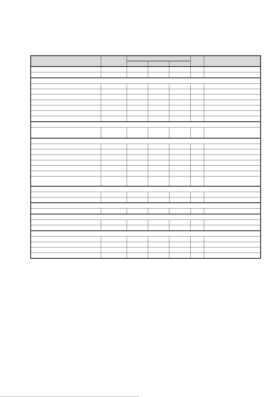
●Electric characteristic
(Ta=25℃, VCC=6.5V, GND=0V,CTL=6.5V unless otherwise specified.)
Parameter Symbol specification value UNIT Condition
MIN TYP MAX
Circuit current 1 IQ1 - 0 10 μA CTL=0V
Circuit current 2 IQ
2
- 3.4 - mA CTL=VCC
< Error amplifier part >
Standard voltage (VREF)V
RE
F
0.792 0.8 0.808 V Terminal FB and FC terminal short
Terminal FB Input bias current IFBB -1 0 1 μA VFB=0.9V
Terminal FC Clamping voltage H VFCH 1.8 - - V VFB=0.7V
Terminal FC Clamping voltage L VFCL - - 0.2 V VFB=0.9V
Terminal FC Sink current IFCSINK 0.5 - - mA VFB=0.9V, VF
C
=0.4V
Terminal FC Source current IFCSOURCE - - -70 μA VFB=0.7V, VF
C
=1.6V
Open loop gain AVER
R
- 100 - dB
<OSC part>
Oscillation frequency FOSC 400 500 600 kHz
When terminal RT 27kΩis
connected
<Soft start >
Charging current ISS -3 -2.5 -2 μA VSS=1.0V
Terminal SS Threshold voltage VSSTH 0.98 1.08 1.18 V VSS Volta
g
e
Terminal SS Clamping voltage VSSCLM 2.2 2.4 - V
Terminal SS Standby voltage VSSSTB 0.1 0.15 - V VSS Volta
g
e(L→H)
Terminal SS Discharge resistance RSS 49 70 91 kΩCTL=0V
Terminal SS Protection circuit start voltage VSSPON 1.0 1.1 1.2 V VSS Volta
g
e(L→H)
Terminal SS Protection circuit start voltage
Maximum hysteresis error VSSPON_HYS 10 100 200 mV VSS Voltage
< Low voltage, over voltage detection part>
Terminal FB Low voltage detection voltage VLV
P
0.51 0.56 0.61 V VFB Volta
g
e
Terminal FB Overvoltage detection voltage VOV
P
0.86 0.96 1.06 V VFB Volta
g
e
< Over current detection part>
Output current limitation threshold Ilm
t
VCC-0.9 VCC-0.7 VCC-0.5 V VSW Volta
g
e
<Power MOS>
Upper side MOS ON resistance RONU - 110 - mΩV
BOOT-VSW =5V
Lower side MOS ON resistance R
O
NL - 110 - mΩV
VREG
5
=5V
<Others>
Terminal PDET L output voltage VOL
_
P
DET - - 0.4 V IOL=100uA
Terminal CTL input voltage H level voltage VIH_CTL 2.0 - VCC V CTL terminal
Terminal CTL input voltage L level voltage VIL
_
CTL - - 0.5 V CTL terminal
Terminal CTL input current II
_
CTL - 60 90 μA CTL terminal, CTL=VCC
VFB : FB terminal voltage, VFC : FC terminal voltage, VSS : SS terminal voltage, VMONVCC : MONVCC terminal voltage
Not designed for radiation resistance.
Current capability should not exceed Pd.

3 / 14
Permissible loss
This package is a product of which the feature is the high heat radiation, and connect the back to GND
based on recommended land pattern when you mount.
Permissible loss : Pd [W]
ROHM standard substrate specification
Material 4 layer glass epoxy substrate(back copper foil70mm×70mm)
Size 70mm×70mm×1.6mmt(Sarmalbiaing is in the substrate.)
Figure 1 Heat decrease curve
※These values are the actual measurement values, and no guarantee values.
θ
jc
[
℃
/W]
θ
j
a
[
℃/W]
T
STGmin
[
℃
]
T
STGma
x
[
℃]
T
a min
[℃]
T
a ma
x
[
℃]
T
cma
x
[
℃]
T
j
ma
x
19.0 31.3 -50.0 150.0 -45.0 85.0 150.0 150.0
Destruction
temperature
[
℃]
Destruction
temperature

4 / 14
●Block diagram
SEQ
Control
VREF
OVP
LVP
OSC
Driver
Control
17
4
6
PROTECT
BUS
I/F
RT
OPEN/SHORT
CTL
10
time
VCC
RT
RSET
PDET
PIO
CTL
SW
SW
PGND
PGND
TEST1
TEST2
PVCC
PVCC
BOOT
VREG5
FC
FB
SS
GND
9 8 7 5
18 19
3
OSC
OSC
VREG5
2 1
N.C.
N.C.
N.C.
N.C.
Figure-2 Block diagram・Application diagram
●Terminal explanation
No. Symbol Description No. Symbol Description
1 PGND Power GND terminal 13 RT
Frequency adjustment resistance connection terminal
2 PGND Power GND terminal 14 RSET
Off latch effective time adjustment resistance terminal
3 N.C. No wire connection.
(Connect to GND. ) 15 PDET Error state notification terminal
4 N.C No wire connection.
(Connect to GND. ) 16 PIO Error state notification
and external IC error detection terminal
5 SW SW terminal 17 CTL Enable input
6 SW SW terminal 18 VCC VCC power supply terminal
7 BOOT High side Power MOS gate drive
power source terminal 19 PVCC Power VCC terminal
8 VREG5 Internal power supply (5.0V) output terminal 20 PVCC Power VCC terminal
9 GND GND 21 TEST2 Test terminal (Connect to GND. )
10 FC Phase amends terminal 22 TEST1 Test terminal (Connect to GND. )
11 FB Feedback terminal 23 N.C. No wire connection.
(Connect to GND. )
12 SS
Soft start adjustment capacity connection terminal 24 N.C. No wire connection.
(Connect to GND. )
※Please give to VCC+0.3V as an operation condition in all input terminals except the terminal BOOT.
However, please do not exceed the absolute maximum rating as VCC=PVCC.
Table 1 Terminal explanation

5 / 14
●Terminal equivalent circuit chart
Terminal
No.
Terminal
name Explanation Terminal equivalent circuit chart
1 PGND
Power GND
(The same potential as the GND
terminal)
2 PGND
Power GND
(The same potential as the GND
terminal)
5 SW SW terminal
6 SW SW terminal
7 BOOT High side Power MOS gate drive power source
terminal
8 VREG5 Internal power supply (5.0V) output terminal
9 GND GND
10 FC Phase amends terminal
PVCC PVCC
PGND
⑤
⑥
VREG5
PGND
⑦

6 / 14
Terminal
No.
Terminal
name Explanation Terminal equivalent circuit chart
11 FB Voltage detection terminal
12 SS Soft start adjustment capacity connection
terminal
13 RT Frequency adjustment resistance connection
terminal
14 RSET Off latch effective time adjustment resistance
terminal
15 PDET Error state notification terminal
VCC
GND
⑪
VCC

7 / 14
Terminal
No.
Terminal
name Explanation Terminal equivalent circuit chart
16 PIO Error state notification and external IC error
detection terminal
17 CTL Enable input
21 TEST2 Test terminal (Connect to GND. )
22 TEST1 Test terminal (Connect to GND. )
19 PVCC Power VCC terminal
20 PVCC Power VCC terminal

8 / 14
●Operation description
ON/OFF control
DC/DC converter ON/OFF function
DC/DC converter controller can be controlled ON/OFF by CTL terminal.
Analog circuit starts operation at ON control (on mode), and goes down to setting output voltage.
Analog circuit should be standby at OFF control (off mode), and output voltage becomes 0V.
Table1 DC/DC converter ON/OFF function
C
TL terminal voltage
>VIHCTL ON control
<VILCTL
O
FF contro
l
Soft start time set function
DC/DC converter can do soft start without overshoot by charging soft start capacity (Css) connected between SS
terminal and GND by charging current at ON control.
The mute of the output is released when it reaches VSS=0.15V (VSSSTB), and the output voltage does the soft start
operation from the point of VSS=0.3V (typ) in proportion to the voltage of the terminal SS.
Also, soft start time (tss) can be set by setting soft start capacity arbitrarily.
Soft start time (tss) should be set at 3msec < tss < 30msec.
※Please note that the overshoot is not caused in the output setting voltage when setting it to tss≦3msec.
SS
ISS
C
SSTH
V
SS
t
Discharge function
DC/DC converter can do soft off by discharging load discharged to soft start capacity connected between SS terminal
to GND by discharging resistance at OFF control.
Soft off operates in proportion to the voltage of the terminal SS the output voltage from the point of VSS=0.8V (typ).
Figure 2 Wave form at ON/OFF control

9 / 14
OSC oscillation frequency setting function
SW output oscillation frequency of DC/DC converter can be set by installing resistance between RT terminal and GND
externally.
Figure 3 Terminal RT resistance-oscillation frequency
Range of terminal RT connection resistance setting
23kΩ≦Rrt≦135kΩ
(100kHz≦fosc≦600kHz)
1
0
10
0
100
0
1000
0
11
0
10
0
100
0
RT terminal resistance[KΩ]
Switching frequency [KHz]
*Reference date

10 / 14
PROTECT BUS Input/output function
The terminal PIO is PROTECT BUS Input/output terminal. The terminal PIO is Hi-Z when DC/DC usually operates. When the
terminal PIO becomes LOW by connecting PROTECT BUS, DC/DC is turned off. Afterwards, when the terminal PIO becomes
HIGH, it reactivates.
DC/DC is Off latch when DC/DC error detects it and the terminal PDET becomes LOW.
Table2 PIO terminal, PDET terminal output function
DC/DC
Error detection PIO terminal PDET terminal DC/DC
Undetection Hi-Z Hi-Z ON
Undetection LOW Hi-Z OFF
Detection LOW LOW Off latch
PROTECT BUS Timing chart
If two or more BD8628EFV/BD8633EFV/BD8624FV/BD8630FV is connected in PROTECT BUS, and it uses at the same time,
when one IC error detects, all remaining IC becomes PIO = Low at the same time, and the output is turned off.
Protecting BUS part timing chart
IC_A
PDET
IC_A
PIO
High
OFF LATCH
When two or more BD8628EFV/BD8633EFV/BD8624FV/BD8630FV is used at the same time,
If one IC error detects, all IC becomes DC/DC OFF at the same time.
IC_B
PIO
DC/DC OFF
IC_B
PDET
IC_A detects error.
IC_B
Vo
High
High
High
LOW
LOW
LOW
0V
PIO
IC_A
PIO
IC_B

11 / 14
●Protection function
Protection circuit is effective for destruction prevention due to accident so that avoid using by continuous protection
operation.
Low voltage protection function(LVP)
Low voltage protection function detects set output voltage VOfrom FB terminal and off-latched DC/DC converter
compared to internal reference level.
Low voltage protection function operates when FB terminal voltage falls below VLVP (=0.7 × VREF) and continues more
than set time in external resistance.
Table 4 Low voltage protection function
CTL
terminal SS terminal FB terminal Low voltage
protection function
Low voltage
protection operation
>VIHCTL >1.1V(typ) <VLVP Enable ON
>VLVP+VLVP_HYS OFF
<1.0V(typ) - Disable OFF
<VILCTL - - Disable OFF
※Constant voltage protection function is enabled when SS terminal voltage becomes more than 1.1V (typ) in the transition
to ON control (during soft start).
Overvoltage protection function (OVP)
Overvoltage protection function detects set output voltage VO from FB terminal and off-latched DC/DC converter
controller compared to internal reference level.
Overvoltage protection function operates when FB terminal voltage exceeds VOVP (=1.2 × VREF) and continues more
than set time in external resistance.
Table 5 Overvoltage protection function
CTL
terminal SS terminal FB terminal Overvoltage
protection function
Overvoltage
protection operation
>VIHCTL >1.1V(typ) >VOVP Enable ON
<VOVP OFF
<1.0V(typ) - Disable OFF
<VILCTL - - Disable OFF
※Overvoltage protection function is enabled when SS terminal voltage of each Ch becomes more than 1.1V (typ) in the
transition to ON control (during soft start).
Figure 5-1.Low voltage / overvoltage protection

12 / 14
Overcurrent protection function (OCP)
Overcurrent protection function compared drain voltage (LX terminal voltage) with internal OCP terminal voltage when
internal Nch POWER MOS is ON. When LX terminal voltage becomes lower than OCP terminal voltage, external MOS
would be OFF.
Off latch by overcurrent protection function operates when LX terminal voltage falls below OCP terminal voltage and
continues more than set time in external resistance.
Table 6 overcurrent protection function
CTL
terminal SS terminal Output current Overcurrent
protection function
Overcurrent
protection operation
>VIHCTL >1.1V(typ) >Ilmt Enable ON
<Ilmt OFF
<1.0V(typ) - Disable OFF
<VILCTL - - Disable OFF
DRV
A
DRV
B
Rocp
LX
OCP
Output
current
Figure 5-2.Overcurrent protection
RT terminal open/short protection function
RT terminal open/shot protection function off-latches all DC/DC converter controller by detecting open/short
condition internally from RT terminal to prevent from output voltage error caused by error oscillation of
internal triangular wave at RT terminal open/short.
RT terminal open/short protection function is regularly enabled after boot-up.
RT terminal open/short protection function operates when error detection condition continues more than set
time in external resistance.

13 / 14
Soft start time-out function
DC/DC converter off-latch-controls when VSS does not exceed VSSPON from VSS > VSSSTB+VSSSTB_HYS after 50msec (typ)
passed from soft start.
Figure 5-3. At soft start time-out
Error detection (off latch) release method
DC/DC converter becomes off latch condition when protection function operates. Off latch can be released by the
following method. DC/DC converter controller of each Ch becomes able to do ON control transition by releasing off latch.
1. Set all Ch CTL terminal voltage as < VILCTL and continue that condition about more than 200usec (typ).
2. Drop down power supply VCC to below 2.7V(TYP).
Error detection time set function
Time from the error detection to the off latch can be set by putting resistance outside between GND and RSET terminal.
sec]u[Rrset.
3
1081
offlatch
t
Rset setting range
10kΩ≦Rset≦75kΩ
(18usec≦tofflach≦135usec)

14 / 14
Catalog No.08T277A '08.8 ROHM ©
<Tape and Reel information>
Ta
p
e
Quantit
y
Direction
of feed
Embossed carrier ta
p
e
2000
p
cs
E2
(The direction is the 1pin of product is at the upper left when you hold
reel on the left hand and
y
ou
p
ull out the ta
p
e on the ri
g
ht hand
)
HTSSOP-B2
4
(
Unit:mm
)
<Dimension>
12
1324
1
0.08
M
0.08 S
+0.05
+6
−4
−0.03
+0.05
−0.04
7.6
±
0.2
1.0Max.
7.8
±
0.1 4
0.17
0.65 0.2
0.325
0.53
±
0.15
0.85
±
0.05
0.08
±
0.05
1
±
0.2
5.6
±
0.1
※When you order , please order in times the amount of package quantity.
Reel 1pin
1234
1234
1234
1234
1234
1234
1234
1234
Direction of feed

Notes
No technical content pages of this document may be reproduced in any form or transmitted by any
means without prior permission of ROHM CO.,LTD.
The contents described herein are subject to change without notice. The specifications for the
product described in this document are for reference only. Upon actual use, therefore, please request
that specifications to be separately delivered.
Application circuit diagrams and circuit constants contained herein are shown as examples of standard
use and operation. Please pay careful attention to the peripheral conditions when designing circuits
and deciding upon circuit constants in the set.
Any data, including, but not limited to application circuit diagrams information, described herein
are intended only as illustrations of such devices and not as the specifications for such devices. ROHM
CO.,LTD. disclaims any warranty that any use of such devices shall be free from infringement of any
third party's intellectual property rights or other proprietary rights, and further, assumes no liability of
whatsoever nature in the event of any such infringement, or arising from or connected with or related
to the use of such devices.
Upon the sale of any such devices, other than for buyer's right to use such devices itself, resell or
otherwise dispose of the same, no express or implied right or license to practice or commercially
exploit any intellectual property rights or other proprietary rights owned or controlled by
ROHM CO., LTD. is granted to any such buyer.
Products listed in this document are no antiradiation design.
Appendix1-Rev2.0
Thank you for your accessing to ROHM product informations.
More detail product informations and catalogs are available, please contact your nearest sales office.
ROHM Customer Support System THE AMERICAS /EUROPE /ASIA /JAPAN
Contact us : webmaster@ rohm.co.jp
www.rohm.com
Copyright © 2008 ROHM CO.,LTD.
The products listed in this document are designed to be used with ordinary electronic equipment or devices
(such as audio visual equipment, office-automation equipment, communications devices, electrical
appliances and electronic toys).
Should you intend to use these products with equipment or devices which require an extremely high level
of reliability and the malfunction of which would directly endanger human life (such as medical
instruments, transportation equipment, aerospace machinery, nuclear-reactor controllers, fuel controllers
and other safety devices), please be sure to consult with our sales representative in advance.
It is our top priority to supply products with the utmost quality and reliability. However, there is always a chance
of failure due to unexpected factors. Therefore, please take into account the derating characteristics and allow
for sufficient safety features, such as extra margin, anti-flammability, and fail-safe measures when designing in
order to prevent possible accidents that may result in bodily harm or fire caused by component failure. ROHM
cannot be held responsible for any damages arising from the use of the products under conditions out of the
range of the specifications or due to non-compliance with the NOTES specified in this catalog.
21 Saiin Mizosaki-cho, Ukyo-ku, Kyoto 615-8585, Japan TEL : +81-75-311-2121
FAX : +81-75-315-0172
Appendix
This manual suits for next models
1
Popular Power Supply manuals by other brands

Atlas Copco
Atlas Copco PP 100 Safety and operating instructions

Elenco Electronics
Elenco Electronics XP-605 instruction manual

Tines & Reeds
Tines & Reeds SideTwix manual

Well Tempered Lab
Well Tempered Lab DPS instruction manual

Honeywell
Honeywell HPL624 Product installation document

CDVI
CDVI PSMB123 instruction manual