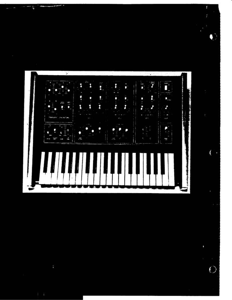
Roland TR-808 Operating and maintenance manual

JUN. 15, 1981 TR-808 FLEXIBLE PCB N-166 SHIELD COVER N-162
BOSS NUT N-524 3x8mm
TR-808 SERVICE NOTES
First Edition
SPECIFICATIONS
Rhythm storage capacity 1-32 steps/measure 64 measures x12 tracks Second Printing (July 12, 1983 E2)
Tempo variable range 4M =40-300
Master output Hi 6Vp-p/1K^2; Lo 0.6V p-p/3Kf2
(Level: Voices @red mark; AC @FCW)
Multi output 1
Trigger output -M5V, 20ms; ^Kn -CB/CP(MA)/AC-
Accent level OdB-lOdB
Power consumption 8W
Dimensions 508 (w) x305 (d) x110 (h) mm
Net weight 5kg
CAUTION
Although some parts are designated in abridged number or numberless in this limited space, they are
fully numbered on the Parts List.
Parts order must be written in full number followed by the part name to encourage prompt,
accurate dispatch.
HOLDER N-247
MAIN BOARD ASS'Y OP31 16-130
HOLDER N-246
S\A/ITCH
SDG5P001 100V
SDG5P001 117V
SDG5P502 220V 240V
POWER TRANSFORMER
N-217N 100V
N-218C 117V
N-219D 220V 240V
LONG NUT N-503 3x 18mm
TOP PANEL REMOVAL SCREWS: ®- ®TERMINAL N-101 TT501 D-1 2P
DUST COVER N-102
SWITCH SQPR24-12P
KNOB N-128
SWITCH SRM-101C
BUTTON N-506 BLACK
PANEL N-242
SIDE PANEL N-118 (L)
KNOB N-128
SWITCH SRM1026
SWITCH DS102 #44
KNOB N-165
POT. GM70EF51E 10KB x2
KNOB N-127
POT. VM10RB10C 50KB
DUST COVER N-115
SWITCH SLE6230
SWITCH W/BUTTON KED 10001
LED TLR124 RED
KNOB N-180 RED
POT EVH-LWAD25B55 500KB
POT EVH-LWAD25C14 10KC
POT EVH-LWAD25A15 100KA
POT EVH-LWAD25B15 100KB
POT EVH-LWAD25B52 500J2B
SIDE PANEL N-119 (R)
POT EVH-LWAD25A53 5KA
POT EVH-LWAD25B24 20KB
POT EVH-LWAD25B26 2MB
DUST COVER N-102
SWITCH SSP04205
POT EVH-LWAD25B14 10KB
KNOB N-128
POT VM10RB10C 50KA
DUST COVER N-115
SWITCH SLP62208
SWITCH W/BUTTON KED10903
KNOB N-167 WHITE
SWITCH KHC11901
KNOB N-168 ORANGE KNOB N-169 YELLOW
(T) —(J)3 X10 mm B1, Fe, Br, Biding, Self tapping
(5) —(7)3x6 mm Fe, Br Binding
TOP PANEL REMOVAL SCREWS
1through 10
SWITCH BOARD ASS'Y OP31 16-090
VOICING BOARD ASS'Y VG31 16-140
JACK BOARD (A) ASS'Y OP31 16-100
JACK BOARD (B) ASS'Y OP3116-110
HOLDER N-248
BATTERY HOLDER N-525
POWER SUPPLY BOARD ASS'Y
OP31 16-051 100V/117V
OP31 16-054 220V/240V
LONG NUT N-501 3x 10mm
CHASSIS N-234
RUBBER FOOT G-7 (111-023) COIN SCREW 3x8mm
RUBBER FOOT G-5 (111-021)
BATTERY COVER N-159
CUSHION N-310
SCREWS (8) —@1 3x6 mm B1, Fe, Br Binding, Self tapping
SCREWS (Q) —@3x10 mm B1, Fe, Br Binding, Self tapping
JACK SG7622 #8(13449106)
SWITCH SSF22-07 (13159112)
(3rd Printing June 1986 C-2) Printed in Japan AE2 1

TR-808 JUN. 15, 1981
(Top View) pPDAAAC
As 118
As c217
316
Aa 1415
Ao 1514
A, c613
A2 712
CS 811
GND 910
HM4334P-4
1024-word
X
4-bit Static CMOS RAM
As
Ah
Ab
A:
As
IOi
I02
I03
I04
cs
\VE
,mmm
c-+~V0 IN 0-^V
U®U
©i
nnnnriryf
I^W
[
/IJ ULi Jli LJ'ir^
<7L
MC14001BCP
Quad 2-Input NOR Gate
TA7179P
DUAL ±15V TRACKING RAGULATOR
GND
BALANCE
+COMPEN
+SENSE
+VOUT
NG
VCC
VOLTAGE
ADJUST
NC
-COMPEN
-SENSE
-VOUT
NC
VEE
Heg.IN =5raV( typ) (VIN=18-30Vj
Reg. OUT= 5mV (typ) (I0lJT=0-50raA}
Ripple rejection ratio =75dB
Output current =100mA (max)
n-T fOUTPUT
COMMON
INPUT
ORDER INFORMATION
OUTPUT
VOLTAGE
5V
6V
8V
8.5 V
12 V
15 V
18 V
24 V
TYPE
44A7805C
MA7806C
MA7808C
MA7885C
MA7812C
mA7815C
mA7818C
mA7824C
PART NO.
MA7805UC
31A7806UC
MA7808UC
44A7885UC
MA7812UC
MA7815UC
44A7818UC
^A7824UC
HA7800 SERIES
3-TERMINAL POSITIVE VOLTAGE
REGULATORS
ABSOLUTE MAXIMUM RATINGS
Input Voltage (5 Vthrough 18 V)
(24 V)
Internal Power Dissipation
Storage Temperature Range
Operating Junction Temperature Range 4iA7800
/4A7800C
Lead Temperature (Soldering, 60 stime limit) TO-3 Package
(Soldering, 10 stime limit) TO-220 Package
35 V
40 V
Internally Limited
-65°C to +150°C
-55°C to +150°C
0“C to +150°C
300° C
230°C
HD14584B MC14051B
8-Channel Analog
Hex Schmitt Trigger Multiplexer/Oemultiplexer
Vdd ’Pin 16
Vss =Pin 8
Vg g-Pin 7
AN69I2
Quad
Comparator
0UTPUT2|T
OLFTPUTl H
V-[3
TRUTH TABLE
1Control Inputs ON SwitchesSelect
Inhibit cBAMC14051B MC14062B MC14053B
0000xo YO XO ZO YO XO
00 0 X1Y1 XI zo YO XI
0 0 10X2 Y2 X2 ZO Y1 XO
0 0 11X3 Y3 X3 zo Y1 XI
0100X4 Z1 YO XO
0101X5 Z1 YO XI
01 1 0X6 Z1 Y1 XO
0111X7 Z1 VI X1
1XXXNone None c0
2
'Not applicable for MC14052
X=Don't Care
MC14051B FUNCTIONAL DIAGRAM
BLOCK DIAGRAM MC14013B
BA662
CJiD
/•£xUinnjQjm
CWT
)llj'ilj l!i LlL ITtT
y
-<JV
TC4011BP
Quad 2-Input NAND Gate
IN+
onn n n.
)LC OTJ4
IN ^
/^PC 4558 C
DUAL TYPE DFLIP-FLOP
TRUTH TABLE
Vdd 'Pin 14
Vss ”Pin 7
INPUTS OUTPUTS
CLOCK* DATA RESET SET Q Q
00001
_r~ 10010
X0 0 QQ
XX1001
XX0110
X X 1111
X-Don't Care
T=Level Change
2

TR-808
JUN. 15, 1981
TR-808 CIRCUIT DESCRIPTION
FIGURE 1BLOCK DIAGRAM
MPD650C-085 FUNCTIONAL DESCRIPTION
No,
PH 0
(PortH) 1
2
3
26
27
28
29
Scanning signal outputs to switches
Switching signal outputs to STATUS BUFFER &GATE
PA 0
(Port A) 1
2
3
33
34
35
36
Switch scanning signal inputs
STATUS (TEMPO. CLOCK. START/STOP. FILL IN) inputs
PB 0
(Port B) 1
2
3
37
38
39
40
Inputs from STEP Switches (RHYTHM SELECT Swtiches)
PG 0
(PortG) 1
2
3
22
23
24
25
Drive signals to STEP LEDs
PE 0
(Port E) 1
2
3
12
13
14
15
1st/2nd CP
A/B RS
Memory bank HT
select MT
MEMORY ADDRESSES CH INSTRUMENT DATA
p. .These pins use CE from qu These data need
n^umbeTs ADDRESS Decoder to ^COMMON TRIG to
select cells in RAM to trigger Sound Generators
be accessed CB being designated
LT
Step SD
numbers BD
AC
PD 0
(Port D) 1
2
3
8
9
10
11
PF 0
(Port F) 1
2
3
16
17
18
19
PC 0
(Port C) 1
2
3
2
3
4
5
Data Inputs/Outputs
PI 0
(PortI) 1
2
30
31
32
Memory WE
Memory CE (associated with PE-2, 3at ADDRESS DECODER)
Trigger Pulse (INSTRUMENT) output
General
As can be seen from the block diagram, most processes of TR-808 up
to generation of pulses triggering sound generators are controlled by
the computer. CPU pin functions are as shown at the lower left table.
Once power is turned on for TR-808, pulses are generated from PI-2
of CPU regardless of TR-808 function mode (Start/Stop) and of
presence or absence of rhythm patterns. The time length between
the pulses is equal to that of the shortest rhythm patterns. The pulse
is transfered to TRIGGER MONO, then ACCENT from which it is
applied in parallel to ail the gates prestaged to Sound Generators;
accordingly, called COMMON TRIGGER. On the other hand, instru-
ment data designating sound to be outputted are independently
supplied to the gates from corresponding exclusive ports (PD, PE
and PF). Since Instrument data are time sharing the data buss with
memory addresses, the data are aligned with Common Trigs in timing.
When these two signals are applied, the gate ANDs the two signals
and outputs asignal triggering the sound generator. Since the peak
value of this trig signal is in proportion to that of the
Common Trig pulses, when an accent data is outputted, the data
can be used to change the amplitude of the Common Trig signal.
Panel control settings are read by interruption of CPU each time
an interrupt signal is fed to the INT terminal. First, the Buffer &
gate turns on by asignal from PH, and the status is read through PA.
Then, some statuses of function switches are read through PA by
asignal from one port of PH. At the same time, some statuses of a
group of step switches are read through PB, and the step LED drive
signal is outputted from PG as required. Statuses are read each time an
INT signal is fed. However, statuses of the step and function switches
are read every four times of INT signals.
Four CMOS RAMs (IK x4-bit) are used for data storage. Chips are
selected when the upper two bits of PE data decoded by IC5 are
enabled by pulses from PI-1. Addresses of chip memory cells are
designated by bits of PD, PE and PF. Data storage to addresses are
possible when an L output from PI-0 is applied to WE
.
Detail
SW Scanning, Status Reading
Reading of statuses of the controls on the panel (step switches,
function switches, tempo, etc.) starts when an interrupt signal is
applied to INT terminal every 1.9ms. When the signal is applied to
INT terminal, CPU starts interruption. The interruption period is
approx. 600/us. During the first 150/us, PHO—PH3 become H, and
the collector of AND gate Q18 becomes L. STATUS signals are
ANDed with this Lby ICS and read through PA. After 150jus, only
PH-0 becomes L. This signal is converted to Hby Q23, and reaches
PB and PA through the closed contacts of the Step switches (No. 1—
No. 4), SWla (Mode) and SW2 (Clear). When one of the four Step
switches is closed, the corresponding STEP LED lighting signal is
immediately fed from PG. Since the PG output is latched until the
next INT signal is applied, the lighting period is approx. 1.8ms. This
period bis approx. 450/us. The remaining period cis for processing
of main program. When the next INT signal is applied, PHO—PH3
become Hagain, the statuses of the TEMPO CLOCK, START/STOP,
TAP, etc. are read again. Then, only PHI becomes Land the statuses
of switches connected to the collector of 024 are read. At the next
INT signal, STATUS and PH2 become L. Next, PH3 becomes L.
This change is repeated. In this way statuses are checked each time an
INT signal is applied every 1.9ms so that the CPU can respond to the
status change promptly. The statuses of other switches are read every
four times of INT signals. This corresponds to one reading every
7.6ms.
INTERRUPT
CLOCK
ICl pin 61.9ms
PHO
PHo
7.6ms
PHI
pin 26
PH2
PH3
150us
STATUS
gate
active low
STEP 1-4
MODE
CLEAR
STEP 5-8
PRESCALE
BASIC VARI,
STEP 9-12
INSTR. SELECT
INSTRUMENT
SELECT
STEP 13-16
AUTO FILL IN
I/P VARIATION
TEMPO CLOCK
START/STOP
TAP
FIGURE 2
INTERRUPT CYCLE
TIMING DIAGRAM
INTERRUPT
CLOCK
PH
600us
1
ab1
I
450/u.s
STATUS
GATE
All time lengths
are approximate.
15QU.S
3

TR-808 JUN.15,1981
CPU PI-1_
Memory CE
lO^S lOjULS lO^s
VALib ADbRESB
READ CYCLE
IC7-IC10
pins 11-14
PC 0-3
Data read
STORED DATA]
1
2
3
RAM, Address Decoder
Four static CMOS RAMs (juPD444C, IK x4-bit) are used for memory.
The memory map is shown in Fig. 4.
The upper two bits PE2 and PE3 of CPU designate aRAM, IC5
decodes these bits, and the memory select is enabled by asignal from
PI-1 (CE). See Fig. 5.
Cell addresses are designtated by bits from PD, PE and PF. After 'lOfj.s
of CE, the data shown in Fig. 5-2 is read (5-3) or anew data from
PC is written (Fig. 5-5).
As can be seen from Fig. 5-2 and -4, during writing, PC output data
and RAM data at the I/O ports of RAM may conflict with one
another. To prevent this, the buffer resistors (R85—R88) are con-
nected.
The LED driver transistors (Q2-Q5) for BASIC VARIATION, 1ST
and 2ND are directly connected to the bus of PD and PE. However,
since various data appear on the bus by time sharing processing, the
LEDs may sometimes light even when unnecessary signals are applied,
resulting in possible lighting timing disparity in amode.
RAMs' low power consumption during high CE allows memories to
be maintained for longer period with back-up battery.
Trigger Gate
Pulses corresponding to the shortest rhythm step usable by TR-808
are fed from PI-2 of CPU at atime interval determined by the setting
of TEMPO CONTROL (Fig. 6-1). On the other hand, instrument
data to be reproduced are applied from PD, PE and PF to the gate
of each sound generator in synchronization with step pulses (Fig. 6-3).
Since the step pulse width of 10)Us is too narrow to trigger asound
generator, it is widened to approx. 1ms which is nearly equal to the
width of instrument data signal. This widening is accomplished by
the monostable IC6. It is triggered by arising edge of 027-inverted
pulse. (Fig. 6-2). The Lperiod is determined by the sum of the
time constants of R100 xC23 and R102 xC27.
The output from pin 10 of ICO passes through the ACCENT circuit
composed of Q31—Q34, becomes aCOMMON TRIG signal, and
simultaneously applied to the gates of all sound generators in parallel.
When instrument data is present at agate, this trigger signal is ANDed
with the data and activates the corresponding sound generator (See
Fig. 7).
Since the AND output from the gate is in proportion to the amplitude
of the common trig signal, the output of the sound generator has the
amplitude in proportion to the common trig signal. Accordingly,
when ACCENT data are present, they are added to the common trig
signal. Since the output of pin 10 of IC6 is anegative logic signal,
when there are no step pulses, the output signal becomes H, Q31
turns on and places aground at base of Q32. When pin 10 of IC6
becomes L, Q31 becomes off, and when ACCENT data from PF-3
is L(no accent), Q34 turns on to shunt VR3. As aresult, the base of
Q32 becomes approx. -i-5V and trig amplitude is approx. 4V. When
ACCENT data is H, avoltage between 5V and 15V according to VR3
setting is applied to the base of Q32, and is converted into trig pulses
of approx. 4—14V. This explains that ACCENT level can be changed
by VR3.
In the case of CB, CY, OH and CH, trig variation range is narrowed
to 7V—14V by 1/2 IC2 (pins 1—3) on the voicing board to increase
S/N ratio.
STELE FIGURE 6
INSTRUMENT TRIG-INSTRUMENT DATA TIMING
DATA
WRIT^ CYCLE 4
FIGURE 7VOICE GENERATOR TRIGGER PULSE
FIGURE 5READ/WRITE CYCLE TIMING
4

JUN. 15, 1981
Start Stop
START/STOP STATUS
Q12 collector
^TEMPO CLOCK -]
Q15 collector |
ICl pin 1
ICl pin 2
IC2 pin 4
IC2 pin 6
ICl pin 13
ICl pin 12
Ql6 ON (charge)
FIGURE 9TEMPO CLOCK TIMING DIAGRAM
TR-808
START/STOP &Tempo Clock
When the power supply for TR-808 is turned on, the TEMPO clock
continues oscillation regardless of the operation mode of TR-808.
However, when the START button is pressed in the STOP mode,
oscillation stops once for 9ms to provide amode change preparation
time to CPU. In this way, the START/STOP circuit and the TEMPO
circuit are closely related with each other. When the SYNC IN/OUT
switch is set to IN, both circuits become ineffective and externat
signals from the DIN socket duplicate the both circuits.
When the START/STOP switch is pressed (closed) with rhythm
stopped, Qof F/F IC2B becomes L,*the collector of 012 becomes
H, 0of IC2B becomes Hand IC2A is reset. 0of IC2A becomes H
and the collector of 015 becomes L. Then, since 0of IC2B becomes
H, pin 2of ICl becomes Lto turn on 016. As aresult, the TEMPO
GENERATOR of 2/4 ICl (D, E) stops oscillation (details are de-
scribed later). After 9ms later, pin 1of IC1A drops below the thresh-
old level and pin 2is reversed. The rising edge reverses 0of IC2A to
Land the collector of 015 (TEMPO CLOCK output) becomes H.
At the same time, 016 is cut off, and C10 starts discharging through
the ANTI-LOG 014 to continue oscillation.
This discharging speed of CIO determines the oscillation frequency of
the TEMPO clock. The variation range is between 8.3ms and 65ms.
With TR-808, Jis defined to have 24 clocks, and thus Jis
approximately equal to 400—300.
Wheri the level of C10 exceeds the threshold level of pin 13 of ICl
due to discharging, the output of pin 10 is reversed, 016 turns on,
and CIO is charged. The output of pin 12 of ICl is divided into 1/2
by T-FF of IC2A.
The bridged T-network filter shown in Fig. 11 is used to generate
periodic damping drum sound. This configuration has variations
according to application (instrument sound). Values of Rand C
can be changed. With this circuit, the decay time becomes longer as
Oincreases.
The swing type VCA shown in Fig. 12 is used to generate metalic
sound (noise). This circuit features its output waveform having
many high harmonic components to provide ringing metalic sound.
Major features of each sound generator are described below.
Bass Drum
.This sound generator is composed of amulti-feedback, bridged
T-network including 1/2 IC12 (pins 1—3) as an active element. The
decay time of the resonating waveforms can be controlled by ad-
justing feedback amount by VR6.
Immediately after atrigger pulse is fed into the generator, the filter's
time constant -when ACCENT is present -is halved and has a
resonance on twice its inherent frequency for ahalf cycle period,
then on the fixed frequency with decaying amplitude. This changing
frequencies will sound apunchier crisp bass. This trick is performed
by the circuit composed of Q41—Q43.
When atrigger signal is outputted from the collector of Q40, Q41
turns on, Q42 turns off, Q43 turns on and R165 is shorted. This
halves the time constant of this network. The ON period of Q43
is determined by R156 and C38 and equals 4ms which is 1/2 x1/2
of 16ms of the inherent oscillation period of the filter.
When Q42 tgrns on after 4ms, current discharging from C39 via
R161 produces aretriggering pulse. At this time the generator oscil-
lates on the inherent frequency.
Muting, Reset
The circuit composed of Q10—Q12 detects power on/off or sharp
voltage drops in TR-808 DC lines and feeds forward bias (0 volts) to
FET switches connected to point A. These FETs are for resetting
CPU (Q64), preventing writing into RAMs (Q75) and muting Master
Out (Q13).
Power on: 0V1-2sec—15V
Power off: —15V to OV
If this circuit is defective, the CPU may be kept reset. (Detail in
TROUBLESHOOTING on page 14.)
FIGURE 12 REPRESENTATIVE SWING TYPE VCA
Sound Generators
5

TR-808 JUN. 15,1981
Snare Drum
This sound generator has two bridged T-networks for fundamental
waveforms and harmonic waveforms. The output ratio of the two can
be changed by VR8 to tailor sound characteristic. The amplitude of
snappy envelope can be controlled by VR9.
LT/LC (MT/MC, HT/HC)
These three sound generators are composed of the circuits based on
the same principle. LT/LC is described below as an example.
This sound generator is composed of amulti-feedback, bridged T-
network including IC5 as an active element. Voices are switched by
SW8 (C77 —frequency, R224 —level). While the oscillation is large
in amplitude immediately after triggering, it is on ahigher frequency
due to conductions of D80 and D81, which reduce time constant of
the filter. As the resonance is damped, its frequency is lowered by
the effect of increasing diodes' internal resistance. Timbre variations
corresponding to time elapse will appreciably be heard as in the case
of Bass Drum.
Pink noise with aslightly longer decay time is mixed for Low Tom
Tom to provide artificial reveberation.
RS/CL
CL Output from multifeedback bridged T-network incorporated
with IC20 is routed to IC19. Output from IC21 (for RS), also routed
via R320, can be ignored because of its minimized level due to im-
pedance imbalance at pin 7of IC20b.
RS Disconnected R313 makes IC20b just as a buffer for CI20a
output. The output of IC20b is applied to 062 together with the
output of IC21. The envelope applied to 062 is formed by R107
and C24. As described in the beginning of this section, VCA of this
type is intended to provide many high harmonics in the output
signals.
Normally-conducting 074 remains off only while trigger pulse is
transferred from 061 to allow IC19 to pass signals. This switching
is provided to eliminate noise leaking from IC20, especially for
CL —relatively large amount, being wired for high O.
CP/MA
White noise passed through the band pass filter (IC21) is applied
to two VCAs in parallel to have different envelopes. These envelopes
are combined tp obtain sound source for the CP sound generator.
Since an envelope with arelatively long decay time is applied to the
VCA Q70, output from this VCA constitutes reverberation of CP
sound.
The output envelope at the VCA (IC22, Q71 and Q72) is aunique
sawtooth shape, and is amain component of this sound generator.
The sawtooth envelope generator circuit is mainly described below
to explain its rather complicated operation. When trigger pulses are
applied to pin 8of the quad comparator IC23, the output is inte-
grated by R350 and Cl 40, and converted into pulses of 30ms wide
as shown in Fig. 13-2. At the falling edge of the pulse, pin 13 of
IC23 becomes H(Fig. 13-3). The output from pin 1of IC23 is also
applied to pin 4of IC23, pin 2of IC23 becomes from —15V to OV,
IC23 OV
pin 14(7)
-15V
OV
IC23
pin l(lO)
IC23
pin 13
0144
-15V
-15V
OV
-15V
IC23
pin 2
OV n5
-15V -j
IC23
pin 5
IC22 pin 87
FIGURE 13 HAND CLAP GENERATING CYCLE
Q73 turns on, pin 5of IC23 becomes —15V, pin 2of IC23 returns
to —15V, and Q73 returns to off state. Accordingly, the output
waveform at pin 2of IC23 becomes narrow pulses as shown in Fig.
13-5,
The moment Q73 is turned on, C144 is abruptly charged to —15V.
However, immediately after charging, Q73 turns off and the charges
are discharged through R365 and D71. When the level of pin 5of
IC23 becomes higher than the level of pin 4due to discharging, pin
2of IC23 reverses again and C144 is recharged to —15V. After this
process is repeated and advanced to the middle of the third time,
pin 1of IC23 rises to OV. This signal is differenciated by R357 and
C141, and the generated pulse turns on Q73. At this time, although
the terminal voltage of C144 rises gradually from —15V due to
discharging, pin 2does not reverse since pin 4of IC23 has reached OV.
The output (Fig. 13-4) of this envelope generator is applied to the
base of Q72 and converted exponentially by Q72 together with the
signals applied to the base of Q71 (offset adj. signal from TM3 and
accent signal via D68, C143 and R362. The converted signal is applied
from the collector of Q72 to pin 1of IC22 to change the amplitude
of noise from the filter IC21.
Note: IC23 (AN6912) is constructed with open collector NPN transis-
tors for output and operates on single (negative) power only.
MA White noise is gated by Q65 and supplied to the same buffer
IC19 as for the CP sound generator through the filter Q68. Envelope
for MA sound generator is generated by Q66 and Q67.
CB
This sound generator uses the outputs of two square waveform
oscillators with different frequencies (by Schmitt triggers). Each
oscillation output passes the corresponding exclusive gate (VCA,
Q14, Q15) and mixed by the filter IC2.
Aseries of R82 and C34 connected in parallel with C9 forms an
envelope having abrupt level decay at the initial trailing edge to
emphasize attack effect.
CY
The combined square wave outputs of six Schumitt triggers including
two for CB generator is separated into high and low range components
by two filters composed of IC3. The high range component from pin
7of IC3 is further separated into two frequency ranges. The output
of the gate Q16 has the highest frequency component of this sound
generator. Its decay time is short. The output of Q17 is in afrequency
range slightly lower than the above output, and its decay time is
controllable.
These three signals with different frequency ranges are outputted
with their level ratio controlled by VR4.
OH
The high frequency range component signal obtained by the above
1/2 IC3 is gated by Q27 and supplied to the buffer IC7 through the
filter Q26. When the CLOSED HI-HAT (CH) is triggered while the
OH circuit is activated, 023 turns on by the voltage applied through
R173. At this moment, the decay time of the OH circuit terminates.
CH
This shares the same sound source with the OH. The signal is gated
by 030 and supplied to the filter 031 and the buffer IC7 (1/2).
6
JUN. 15, 1981
POWER SUPPLY

TR-808 JUN.15,1981
JACK-A MAIIM BOARD si'is-'iso FROM POWER SUPPLY
JC400/BCP
8

TR-808
JUN. 15, 1981
CK)
C.P.TRIG
ooo
9

“il
iS
TR-808
MAIN BOARD
OP3116-130 (7311613006)
(pcb 291-400A)
COMPONENT SIDE
JUN. 15,1981
SWITCH BOARD
OP3116 090 (7311609000)
(pcb 291-402)

AUTO FILI
“mjjtin'
T5MPO:

TR-808 JUN.15,1981
POWER SUPPLY
PS3116-051 (7311605100) 100/117V
PS3116-054 (7311605400) 220/240V
(pcb291-405A)
910 11 12 13 14
IJACK BOARD B
OP3116-110 (7311611000)
I(pcb 291-404)
COMPONENT SIDE VOICING BOARD VG3116-140 (7311614001) FOIL SIDE
(pcb 291 -401 A)
TONE
VR4
R)02
RlOO
R99
MUTING
12


ADJUSTMENT
TR-808 JUN. 15,1981
ADJUSTMENT Connect Set Adjust Reading
CPU CLOCK scope to
TP-1 IFT-L 2us/cycle( 500kHz)
check 4V p-p
INT
CLOCK scope to
TP-
2
TM-1 1.9ms/ cycle
TEMPO
CLOCK scope to
TP-
3
TEMPO. FINE :FCW TM-2 8.33ms/cycle
TEMPO: FCCW
FINE :FCW check 65ms+5ms/cycle
NOISE
GENERATOR AC volt-
meter to
TP-4
TM-4 130mV rms
CP (HAND
CLAP)
OFFSET
scope to
TP-
5
write, play CP
at atempo w/
LEVEL FCW TM-3 .//rO;...,,
...
I
CB (COW
BELL)
FREQUENCY
scope to
TP-6 TM-1 1.85ms/ cycle
TP-7 TM-2 1.25ms/cycle
TROUBLESHOOTING
This section describes funda-
mental approach to isolate
defective circuits or compo-
nents .
Although most TR-808 circuits
function under the CPU control,
possible reasons will ofcen be
found on peripheral circuits.
Replace CPU last of all.
Some useful information can
be derived from the circuit
description.
CHECKING VOICES
-Refer to right-hand table -
Connect scope to the MULTI OUT jack of aVOICE.
When observing amplitude, set ACCERT LEVEL to FCCW position
and the VOICE LEVEL to ECW ,then turn ACCENT ECW .DECAY,
TONE, etc. for that voice must be set at 12 o'clock.
AMPLITUDE FREQUENCY DECAY TIME
NORMAL ACCENT LOW MID HIGH SHORT MID LONG
Vpp Vpp ms
(Hz) ms
(Hz) ms
(Hz) ms ms ms
BD 3.5 10 —18
(56) —50 300 800
SD H
L
310 —2.1
(476) ——60 —
4.2
(238)
LC 3.5 12 6.1
(165)
5.4
(185)
4.5
(220) —180 —
LT 3.5 12 12.5
(80)
11.1
(90)
10
(100) —200 —
MC 310 4
(250)
3.6
(280)
3.2
(310) —100 —
MT 311 8.3
(120)
7.4
(135)
6.3
(160) —130 —
HC 3.5 12 2.7
(370)
2.5
(400)
2.2
(455) —80 —
HT 3.5 12 6.1
(165)
5.4
(185)
4.5
(220) —100 —
C2.5 8—0.4
(2500) ——25 —
RS
L
310 —0.6
(1667) ——10 —
2.2
(455)
M35———25 —35
CP 62————100 —
CB H
3.5 12 —1.25
(800) ——50 —
L1.85
(540)
CY 3.5 7———350 800 1200
OH 3.5 7———90 450 600
CH 36————50 —
values are typical and variable
DC SUPPLY
Confirmation of DC supply voltages is the first thing to
be done in troubleshooting. Check +5V, +15V and back-up.
CPU is forced to reset and is not allowed to restart when
DC source is so irregular that Voltage Change Detector
keeps reset signal.
Lower impedance load connecting to voice output jack can
draw relatively large current through op amp when the
so'’und level is high. The sum of the currents, when many
louder voices are outputted in step, flowing into these
loads would cause DC source to drop enough below the De-
tector sensing level. To make sure of this, pull all
plugs off the jacks. Contrast to the above is ashort-
circuitting IC .One short circuit in astage only could
not be sensed by the detector since "B" supplied to a
particular circuit group is independently filtered, or
rather, the short circuit will increase ripples in the
line, causing TEMPO CLOCK to be unstable.
STATUS, SWITCH SCANNING
Each port at PH routes scanning signal to the switches
connecting to its bus. PA and PB read signals coming via
the switches. If aswitch is misread, check scannings for
other switches: one sharing the same PH bus, one sharing
the same input port -with corresponding switchings.
RAM STORED DATA
As shown in memory map on page 4, aRAM is partitioned
into blocks. It is unlikely to occur in aRAM that only
one block fails to handle data when the RAM or the De-
coder malfunctions. For example, if all instrument data
but Cow Bell enter IC8, similar phenomenon might true to
other RAMs ,were the troubles through PC-0 bus.
TRIGGER PULSE
Lack of trigger pulse from agate is not what Common
Trig is responsible for, when other sound generators are
fired
.
Common Trig with pulse width longer or shorter than 1ms
will be acause of deteriorative voices.
14

JUN. 15, 1981
DESIGN CHANGES &IMPROVEMENTS
TR-808
The reasons for modifications will help to remedy the problems as
described below, may be found on early TR-808.
Some of the modifications were done at the factory on some products
bearing serial number earlier than indicated:
MAIN BOARD -modification 1, 4
VOICING BOARD -modification 1
MAIN BOARD
EPT’ECTIVE WITH
SERIAL NUMBER PART AFFECTED REASON (* SOLUTION)
1000300 INT CLOCK
ICl (HD14584)
1>0.047
Oil 0.068-^Q^Q3g
(C203)
Variations in HD14584 hysterisis
sometimes deviate Clock Rate out of
specified frequency range.
*To down -0.047+0.039 in parallel
*To up -remove 0.039
2010600 CP (Hand Clap) IC21
R346 IK >680
R332 22K >27K
CP sound overmatches the rest in level.
*Reduce the gain
(Both proper and reverberation
components .
)
3010600 CPU (pin 30)
R91 15K >IM
Small resistance allows CPU to draw
relatively larger current from back-
up batteries with MODE selected other
than PLAY or MANUAL PLAY in Power OFF.
*Increase resistance
4
010600
DIN SOCKET
(pin 5)
R25 220K >1.5M Reject unnecessary signals from
external circuitry to prevent false
triggering at subsequent stage.
*Increase resistance
CPU (pin 37)
Capacitor 0.01 across
DIN pin 2and chassis
Grounding
Protect CPU against static electricity
build-up at external circuitry.
*By pass charge
5010600 NOISE GENERATOR (IC24)
R129 330K >short
R311 330K >100K
R127 4.7K->10u(C200)
C202 0>22p
Variations in UPC4558 bias current
are transferred to l/2 IC24 output as
an offset reducing gain margin.
*Decouple DC
MAIN BOARD cont'd
EFFECTIVE WITH
SERIAL NUMBER PART AFFECTED REASON (* SOLUTION)
6010600 VOICE GATE
R106, 1^154, R182, R213
,
R242, R268, R298
22K >lOK
Ensure sufficiency of gate drive signal
voltage at lower COMMON TRIG amplitude.
*Increase gain
7010600 COMMON TRIG
IC6 (TC4011BP)
RlOl lOK >lOOK
C201 0>22p
High frequency from CP generator induces
irregular oscillation on other generators
triggered at the same time.
*Filter out CP high frequencies
8020800 START/STOP (IC2)
CPU (pins 7, 31)
Q64,Q75 0>FET
R127 0>6.8K
R54 IM >100K
D32 1>0
Prevent possible disturbance in RAM
memories at power on/off switchings
with MODE set at other than PLAY or
MANUAL PLAY.
*Add PET switches
9031100 LED
SEL2110R >TLR124
Eliminate possible chance of LED D76(D78)
being lit by base current of Q5(Q2).
*Use low sensitive LED
VOICING BOARD
EFFECTIVE WITH
SERIAL NUMBER
PART AFFECTED REASON (* SOLUTION)
1000300 COW BELL (ICl) Difficulty in setting COW BELL sound
C6 00H>0.022 frequency within the specified range.
R44 39OK >150K
R45 33OK >100K *Extend TMl and TM2 control range
2010500 Q1-Q4 To have aclearance between Switch
2SC945P —>2SC2021R Board and transistors' top.
051850 Q5-Q8
2SA733P —>2SA937Q *Employ transistors in shorter package
15

TR-808 JUN. 15, 1981
PARTS LIST
PANEL
2221 024200 Panel N-242 top -
2112511800 Panel N-1 18 side (L, H) (066H021
2112511900 Panel N-119 side (R, H)
2281023401 Chassis N-234 -
111-021 Rubber Foot G-5 rear -
1 1 1 -023 Rubber Foot G-7 front —
SOCKET
13429604 Din connector TCS0250-01 -03 —
13449106 Jack SG7622 #8 mono (009-012)
TRANSFORMER COIL
2245021 7NO
2245021 SCO
2245021 9DO
1244921
7
Power transformer
Power transformer
Power transformer
IFT Coil
N-217N 100V
N-218C 117V
N-219D 220/240V
S74230 yellow CPU clock
SWITCH KNOB
13129101 SDG5P-001 power 100V(001-215)
13129102 SDG5P-001 power 117V (001-216)
13129103 SDG5P-502 power 220/240V (001-217)
13119508 SR Ml 026 rotary mode, auto fill in -
13119806 SRM101C-C rotary instrument/track -
13139129 SLE62301 lever basic variation -
13139128 SLP62208 lever l/F variation -
13159503 SQPR24-12P slide pre -scale (001-228)
13159105 SSP04205 slide instrument (001-293)
13159fl2 SSF22-07 slide sync -
13129901 DS102 #44 push clear (001-045)
13129711 KED10001 key start/stop -
13129703 KED10903 key tap (001-299)
13169601 KHC11901 key step number -
224701 2700 Knob N-1 27 (016-077)
224701 2800 Knob N-1 28 (016-078)
2247016500 Knob N-165 -
2247516700 Knob N-167 white (016H010)
2247516800 Knob N-168 orange (016H012)
2247516900 Knob N-1 69 yellow (016H017)
2247518000 Knob N-1 80 red (016H018)
2247050600 Button N-506 black power switch (016-009)
SEMICONDUCTOR
LSI
15179116 MPD650C-085 CMOS CPU
151 79305 ;uPD444C CMOS RAM
or HM4334P-4 (compatible)
1C
15229802 BA662A Vari-conductance amp.
15159101ZO MC14001BCP Quad 2-input NOR gate -
15159104TO TC4011BP Quad 2-input NAND gate -
151 591 05TO TC4013BP Dual type Dflip-flop -
151591 13ZO MC14051BCP Analog multi/demultipxr -
151 59303 HO HD14584B Hex Schmitt trigger -
15189113 AN6912 Quad comparator -
15199110TO TA7179P ±15V Regulator -
15199106FO MA7805UC -H5V Regulator -
15189105 mPC4558C Dual op amp -
TRANSISTOR TERMINAL
15119105 2SA733 (P) or (Q) -13439119 5045-03A —
15119113 2SA1015 (GR) or (Y) -13439122 5045-06A —
15119806 2SB596 (0) -13439123 5045-0 7
A
—
151291050A 2SC828 (R) selected noise -13439124 5045-08A —
15129108 2SC945 (P) or (Q) -13439110 3022-1 2A —
15129121 2SC2021 (R) or (Q),(S) -13429121 FH1-1 2S-2.54DS —
15129815 2SD880 (0) -13459101 TT501 D-1 2P power cord (042-039)
15139101 2SK30ATM (Y) FET —
15139103 2SK30ATM (GR) FET -
WIRING ASS'Y
LED 2341021000 N-210 3P -
15029103 TLR124 red 2341021100 N-211 3P -
15029119 SEL2110R red S/N up to **10** _2341021200 N-212 6P —
2341021300 N-213 7P —
2341021400 N-214 7P -
DIODE 2341021500 N-215 8P -
15019120 IS2473 Si diode -
15019122 IS188FM Ge diode -
15019236 W-02 rectifier stack -OTHERS
15019209 10E-2 —2246010101 Heat sink N-1 01 (048-001 A)
2215051700 Long nut N-517 3x8mm (120-042)
2215050100 Long nut N-501 3x1 0mm (120-001)
POTENTIOMETER 2215050200 Long nut N-502 3x16.4mm (120-002)
13219310 EVH-LWAD25B52 50012 (B) LT, MT, HT tuning -2215050300 Long nut N-503 3x1 8mm (120-003)
13219311 EVH-LWAD25A53 5K (A) CB level -2215052400 Boss nut N-524 3x8mm (120-052)
13219312 EVH-LWAD25B14 10K (B) AC level, SD, snappy -2219525600 Holder N-256 power switch (064H076)
13219313 EVH-LWAD25C14 10K (C) BD tone -2219024600 Holder N-246 -
13219314 EVH-LWAD25B24 20K (B) CY tone -2219024700 Holder N-247 mein end voicinQ boerd -
13219315 EVH-LWAD25A15 100K(A) level -2219024802 Holder N-248 battery holder -
13219316 EVH-LWAD25B15 100K(B) SDtone -2219510600 Holder N-1 06 Potentiometer (064H055)
13219317 EVH-LWAD25B55 500K (B) BD decay -2219510800 Hpider N-1 08 Power cord (064H074)
13219318 EVH-LWAD25B26 2M (B) CY, OH decay -2219510900 Holder N-1 09 Power cord (064H075)
13219233 VM10RB10C 50K (A) master vol. (028-751) 12199525 Battery holder N-525 -
13219219 VM10RB10C 50K (B) fine (028-762) 2224011500 Dust cover N-1 15 lever switch (065-261)
13219761 GM70EF51E 10K (B)x2 tempo -2224010200 Dust cover N-1 02 slide switch (065-065)
13299114 H1051A013 10K (B) SR19R trimmer (030-<f65) 220201 5901 Battery cover N-1 59 -
13299115 H1051A015 22K (B) SR19R trimmer (030-467) 2202016200 Shield cover N-1 62 main board -
13299117 H1051A019 100K (B) SR19R trimmer (030-471) 2202061201 Protect cover N-612 _
13299119 H1051A021 220K (B) SR19R trimmer (030^73) 2202061701 Protect cover N-617 top panel —
2226031000 Cushion N-310 battery cover -
2216051100 Fiber spacer N-511 power cord terminal -
RESISTOR 12369504 Bushing SR^N-4 -
15229909 ERSC33G561 56012 —12369511 Bushing BU4801 power cord -
12369410 Cord fastener 1702B —
FUSE, FUSE HOLDER
12559104 SGA 0.5A pri.sec 100/1 17V -
12559508 CEE 250mAT pri. sec 220/240
V
-
12199519 Fuse clip TF785 (012-003) Roland has changed parts codings from 6-digit to 8- or 10-digit
"N" followed by abridged number should be used in new coding only.
Ex-code is listed at line end for cross reference.
CIRCUIT BOARD ASSEMBLY
7311613006 MAIN BOARD OP3116-130 (PCB291400A) -
7311614001 VOICING BOARD VG31 16-140 (PCB 291 ^01 A) -
7311609000 SWITCH BOARD OP3116-090 (PCB 291^02) -
7311610000 JACK BOARD (A) OP3116-100 (PCB 291^03) -
7311611000 JACK BOARD (B) OP3116-110 (PCB 291-404) -
7311605100 POWER SUPPLY BOARD PS3116-051 (PCB 291 -405A) -
(100/1 17V)
7311605400 POWER SUPPLY BOARD PS31 16-054 (PCB 291 -405A) —
(220/240V)
CAPACITOR
13639932JO
13589453MO
13589454MO
SL25VB10BP lOjuF 25V
ECQ-UC1A473MC 0.047m F
100/1 17V
ECQ-U2A473MF 0.047mF
220/240V
non -polar
polypropylene
polypropylene
16
Other manuals for TR-808
8
Table of contents
Other Roland Synthesizer manuals

Roland
Roland MC-5DDMKII User manual

Roland
Roland Sound Canvas SK-500 User manual

Roland
Roland XV-88 User manual

Roland
Roland JUNO-DS User manual

Roland
Roland JV-880 Operating and maintenance manual

Roland
Roland JUNO 60 User manual

Roland
Roland XV-5080. User manual

Roland
Roland JD-XA User manual

Roland
Roland GS-500 User manual

Roland
Roland GR-20 User manual

Roland
Roland GR-33 User manual

Roland
Roland JX-305 User manual

Roland
Roland V-Synth User manual

Roland
Roland HP -6 User manual

Roland
Roland GR-33B User manual

Roland
Roland D-20 User manual

Roland
Roland JD-990 User manual

Roland
Roland JUNO-106 User manual

Roland
Roland GR-55 User manual

Roland
Roland FANTOM-6 User manual