Samsung MM-28 User manual

MICRO COMPONENT
SYSTEM
MM-28
SERVICEManual
MICRO COMPONENT SYSTEM CONTENTS
1. Precautions
2. Specifications
3. Disassembly and Reassembly
4. Alignment and Adjustments
5. Special Circuit Descriptions
6. Troubleshooting
7. Exploded Views and Parts List
8. Electrical Parts List
9. Block Diagrams
10. PCB Diagrams
11. Wiring Diagram
12. Schematic Diagrams

ELECTRONICS
© Samsung Electronics Co.,Ltd. March 1998
Printed in Korea
Code no. AH68-20188A

1. Precautions
Follow these safety, servicing and ESD precautions to prevent damage and protect against potential hazards
such as electrical shock and X-rays.
Samsung Electronics 1-1
1-1 Safety Precautions
1. Be sure that all of the built-in protective
devices are replaced.
2. When reinstalling the chassis and its
assemblies, be sure to restore all protective
devices, including control knobs and
compartment covers.
3. Make sure that there are no cabinet
openings through which people--
particularly children--might insert fingers
and contact dangerous voltages. Such
openings include the spacing between the
picture tube and the cabinet mask,
excessively wide cabinet ventilation slots,
and improperly fitted back covers.
4. Design Alteration Warning:
Never alter or add to the mechanical or
electrical design of the unit. Example: Do
not add auxiliary audio or video connec-
tors. Such alterations might create a safety
hazard. Also, any design changes or addi-
tions will void the manufacturer's warran-
ty.
5. Leakage Current Hot Check (Figure 1-1):
Warning: Do not use an isolation
transformer during this test. Use a leakage-
current tester or a metering system that
complies with American National Standards
Institute (ANSI C101.1, Leakage Current for
Appliances), and Underwriters Laboratories
(UL Publication UL1410, 59.7).
With the unit completely reassembled, plug
the AC line cord directly into a 120V AC
outlet. With the unit's AC switch first in
the ON position and then OFF, measure the
current between a known earth ground
(metal water pipe, etc.) and all exposed
metal parts. Examples: Handle brackets,
metal cabinets, screwheads and control
shafts. The current measured should not
exceed 0.5 milliamp. Reverse the power-
plug prongs in the AC outlet and repeat.
6. Insulation Resistance Cold Check:
(1) With the unit's AC plug disconnected
from the AC source, connect an electrical
jumper across the two AC prongs. (2) Set
the power switch to ON. (3) Measure the
resistance between the shorted AC plug and
any exposed metallic parts. Example:
Screwheads, antenna, control shafts or
handle brackets.
If any of the exposed metallic parts has a
return path to the chassis, the measured
resistance should be between 1 and 5.2
megohms. If there is no return path, the
measured resistance should be "infinite." If
the resistance is outside these limits, a shock
hazard might exist. See Figure 1-2
Device
Under
Test
(Reading should
not be above
0.5mA)
Leakage
Currant
Tester
Earth
Ground
Test all
exposed metal
surfaces
Also test with
plug reversed
(using AC adapter
plug as required)
2-Wire Cord
Antenna
Terminal
Exposed
Metal Part
ohm Ohmmeter
Fig. 1-1 AC Leakage Test
Fig. 1-2 Insulation Resistance Test

Samsung Electronics1-2
1-1 Safety Precautions (Continued)
7. Components, parts and wiring that appear
to have overheated or that are otherwise
damaged should be replaced with parts
that meet the original specifications.
Always determine the cause of damage or
overheating, and correct any potential
hazards
8. Observe the original lead dress, especially
near the following areas: Antenna
wiring, sharp edges, and especially the
AC and high voltage power supplies.
Always inspect for pinched, out-of-place,
or frayed wiring. Do not change the
spacing between components and the
printed circuit board. Check the AC
power cord for damage. Make sure that
no wires or components touch thermally
hot parts.
9. Product Safety Notice:
Some electrical and mechanical parts
have special safety-related characteristics
which might not be obvious from visual
inspection. These safety features and the
protection they give might be lost if the
replacement component differs from the
original--even if the replacement is rated
for higher voltage, wattage, etc.
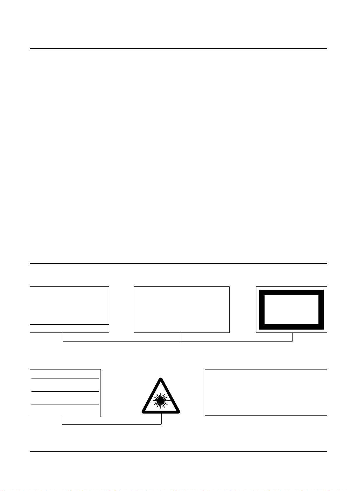
10 Components that are critical for safety are
indicated in the circuit diagram by
shading, or . Use replacement
components that have the same ratings,
especially for flame resistance and
dielectric strength specifications. A
replacement part that does not have the
same safety characteristics as the original
might create shock, fire or other hazards.
1-2 Servicing Precautions
1. Servicing precautions are printed on the
cabinet. Follow them.
2. Always unplug the unit's AC power cord
from the AC power source before
attempting to: (a) Remove or reinstall any
component or assembly, (b) Disconnect an
electrical plug or connector, (c) Connect a
test component in parallel with an
electrolytic capacitor.
3. Some components are raised above the
printed circuit board for safety. An
insulation tube or tape is sometimes used.
The internal wiring may be clamped to
prevent contact with thermally hot
components. Reinstall all such elements to
their original position.
4. After servicing, always check that the
screws, components and wiring have been
correctly reinstalled. Make sure that the
portion around the serviced part has not
been damaged.
5. Check the insulation between the blades of
the AC plug and accessible conductive parts
(examples: metal panels, input terminals
and earphone jacks).
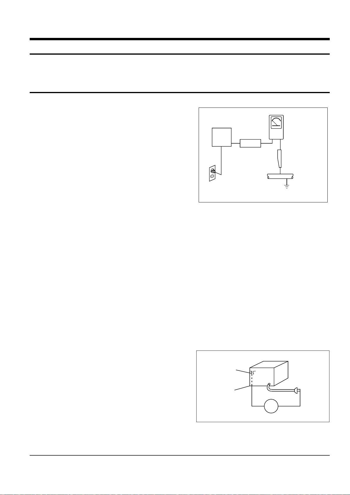
6. Insulation Checking Procedure: Disconnect
the power cord from the AC source and
turn the power switch ON. Connect an
insulation resistance meter (500V) to the
blades of the AC plug.
The insulation resistance between each
blade of the AC plug and accessible
conductive parts (see above) should be
greater than 1 megohm.
7. Never defeat any of the B+ voltage
interlocks. Do not apply AC power to the
unit (or any of its assemblies) unless all
solid-state heat sinks are correctly installed.
8. Always connect a test instrument's ground
lead to the instrument chassis ground
before connecting the positive lead; always
remove the instrument's ground lead last.
Precautions
Warning1: First read the "Safety Precautions" section of this manual. If some unforeseen circumstance creates a conflict
between the servicing and safety precautions, always follow the safety precautions.

Samsung Electronics 1-3
1-3 Precautions for Electrostatically Sensitive Devices (ESDs)
1-4 Special Precautions and Warning Labels for Laser Products
1. Some semiconductor ("solid state") devices
are easily damaged by static electricity.
Such components are called Electrostatically
Sensitive Devices (ESDs). Examples include
integrated circuits and some field-effect
transistors. The following techniques will
reduce the occurrence of component
damage caused by static electricity.
2. Immediately before handling any
semiconductor components or assemblies,
drain the electrostatic charge from your
body by touching a known earth ground.
Alternatively, wear a discharging
wrist-strap device. (Be sure to remove it
prior to applying power--this is an electric
shock precaution.)
3. After removing an ESD-equipped assembly,
place it on a conductive surface such as
aluminum foil to prevent accumulation of
electrostatic charge.
4. Do not use freon-propelled chemicals.
These can generate electrical charges that
damage ESDs.
5. Use only a grounded-tip soldering iron
when soldering or unsoldering ESDs.
6. Use only an anti-static solder removal
device. Many solder removal devices are
not rated as "anti-static" (these can
accumulate sufficient electrical charge to
damage ESDs).
7. Do not remove a replacement ESD from its
protective package until you are ready to
install it. Most replacement ESDs are
packaged with leads that are electrically
shorted together by conductive foam,
aluminum foil or other conductive
materials.
8. Immediately before removing the protective
material from the leads of a replacement
ESD, touch the protective material to the
chassis or circuit assembly into which the
device will be installed.
9. Minimize body motions when handing
unpackaged replacement ESDs. Motions
such as brushing clothes together, or lifting
a foot from a carpeted floor can generate
enough static electricity to damage an ESD.
Precautions
UL : Manufactured for U.S.A. Market.
CSA : Manufactured for Canadian Market.
EU : Manufactured for European Market.
SCAN : Manufactured for Scandinavian
Market.
This Product Complies with
DHHS Rules 21CFR, Sub
chapter J.At date of Manu-
facture
(UL)
(SCAN)
(EU)
CERTIFIED ONLY TO CANADIAN
ELECTRICAL CODE.
CERTIFIE EN VERTU DU CODE
CANADIAN DE LELETRICITE
SEULEMENT
(CSA)
CLASS 1
LASER PRODUCT
(EU)
Fig. 1-3 Warning Labels (Location: Enclosure Block)
Fig. 1-4 Warning Labels (Location: Disc Clamper, Inner Side of Unit Door or Nearby Unit Chassis )
CAUTION : INVISIBLE LASER RADIATION WHEN OPEN
AND INTERLOCKS DEFEATEO AVOIDEXPOSURE TO BEAM
ADVARSEL:USYNLIG LASERSTRÅLING VED ABNING
NÅR SIKKERHEDSAFBRYDERE ER UDE AF FUNKTION
UNDGA UDSAETTELSE FOR STRALING
VARO:AVATTAESSA JA SUOJALUKITUS OHITETTAESSA
OLET ALTTINA NAKYMATTÖMALLE LASERSATEILYLLE ALA
KATSO SATEESEEN!
VARNING:OSYNLIG LASERSTRÅLNING NAR DENNA DEL
AR OPPNAD OCH SPARREN AR URKOPPLAD BETRAKTA
EJSTRÅLEN!

Samsung Electronics1-4
1-4 Special Precautions and Warning Labels for Laser Products (Continued)
1-4-1 Warnings
1. When servicing, do not approach the LASER
exit with the eye too closely. In case it is
necessary to confirm LASER beam emission,
be sure to observe from a distance of more
than 30 cm from the surface of the objective
lens on the optical pick-up block.
2. Do not attempt to handle the objective lens
when the DISC is not on the tray.
1-4-2 Laser Diode Specifications
Material: GaAs+ GaAlAs
Wavelength: 760-800 nm
Emission Duration: Continuous
Laser Output: 0.2 mw (measured at a
1.6 mm distance from the objective lens
surface on the optical pick-up block.)
1-4-3 Handling the Optical Pick-up
1. Static electricity from clothing or the body
may cause electrostatic breakdown of the
laser diode in the Optical Pickup. Follow
this procedure:
2. Place a conductive sheet on the work bench
(i.e., the black sheet used for wrapping
repair parts.) Note: The surface of the work
bench should be covered by a copper
ground plane, which is grounded.
3. The repair technician must wear a wrist
strap which is grounded to the copper sheet.
4. To remove the Optical Pickup block:
Place the set on the conductive sheet, and
momentarily touch the conductive sheet
with both hands. (While working, do not
allow any electrostatic sources--such as
clothes--to touch the unit.)
5. Ground the "Short Terminal" (located on the
PCB, inside the Pickup Assembly) before
replacing the Pickup. This terminal should
be shorted whenever the Pickup Assembly
is lifted or moved.
6. After replacing the Pickup, reopen the Short
Terminal. See diagrams below:
Precautions
THE UNIT
(1) WRIST-STRAP
FOR GROUNDING
1M
1M
CONDUCTIVE SHEET
short
terminal short terminal short
terminal short
terminal
SOH91VI(LDP) SOH91CI(CAR,walkman) SOH94T4N
(CMS-V10,CMS-V30)
SOH-A1
(CMS-V10,CMS-V30)

2. Product Specfications
Samsung Electronics 2-1
General
Amp
Cassette
Tuner
Compact Disc
FM
MW
(AM)
LW
(option)
Power source
Power consumption
Dimensions (mm)
Power output (Front)
Total harmonic distortion
Frequency range
Signal to noise ratio
Channel separation
Frequency range
Usable sensitivity
Signal to noise ratio
IF rejection ratio
Total harmonic distoration
Separation (Stereo)
Frequency range
Usable sensitivity
Signal to noise ratio
IF rejection ratio
Total harmonic distortion
Frequency range
WOW FLUTTER
Erasing effect
Signal to noise ratio
Total harmonic distortion
Frequency response
Signal to noise ratio
Channel separation
Total harmonic distortion
Audio Output
125Hz ~ 12.5KHz
0.2%
50 dB
40 dB
2.5%
20Hz ~ 20KHz(±1dB)
90 dB(1kHz)
75 dB(1kHz)
0.1%(1kHz)
1V (1kHz 0dB)
Frequency range
Usable sensitivity
Signal to noise ratio
146 ~ 290KHz
60 dB
33 dB
87.5 ~ 108MHz
10 dB
50 dB
60 dB
1.5%
25 dB
522 ~ 1611KHz
50 dB
40 dB
33 dB
2%
15W / Ch
0.5% (1kHz)
50Hz ~ 30kHz
70 dB
40 dB
AC 230V 50Hz(Option)
72W
160(W) x 255(H) x 264(D)
Specifications are subject to change without notice.

TIMER
ON/OFF TIMER/
CLOCK
Remote Control

3. Disassembly and Reassembly
3-1 Cabinet-Top, Cabinet-Rear
1. Remove 6 screws of !and 7 screws of @of its rear part
2. Pull its top part upward vertically as shown in the figure 3-1
Figure 3-1
Samsung Electronics 3-1

Figure 3-2
3-2 Samsung Electronics
3-2 Main PCB
Disassembly and Reassembly
1. Pull out the Main-PCB backward horizontally.

3-3 Cabinet-Bottom
1. Remove 3 screws !and pull it out backward.
1. Undo 4 screws of !and then remove the CD-Pack downward.
Figure 3-3
Figure 3-4
3-4 CD-Pack
Samsung Electronics 3-3
Disassembly and Reassembly

Figure 3-8
3-4 Samsung Electronics
3-6 CD Deck
1. Remove the Shaft !.
2. Lift the P/U @.
Note : Take extreme care not to touch the surface of lens.
If there is an alien materials, clean it with swab smeared alcohol.
3. Lift the Center-Knob #.
4. Remove the Center-Ring $.
5. Remove the Spring-T/Table %.
6. Remove the Turn-Table (M) ^.
7. Remove 2 screws &and then remove the Spindle-Motor *.
8. Remove the Cover-Gear (by pushing the hook.
9. Remove the Gear (c) )by pushing the hook.
10. Lift the Gear(b) 1.
11. Remove the Gear(a) 2.
11. Remove 2 screws 3and the then remove the Feed-Motor 4.
12. Remove the Chassis-Deck (M) 5.
Disassembly and Reassembly
4
6
713
21
9
10
11
12
14
15
8
3
5

4. Alignment and Adjustments
4-1 Tuner
Samsung Electronics 4-1
FM T.H.D Adjustment
Minimum Distortion (Figure 4-1)
SSG FREQ.
Adjustment
point
(IFT2)
Output
98 MHz
FM DETECTOR COIL
60 dB
AM(MW) I.F Adjustment
SSG FREQ.
SET FREQ.
Adjustment
point
(IFT1)
450KHz
522 KHz
AM I.F COIL
FM Search Level Adjustment
Adjust IVR1 so that “TUNED” of FLT is
lighted (Figure 4-2)
Maximum output (Figure 4-3)
Figure 4-2 FM Auto Search Level Adjustment
Figure 4-3 AM I.F Adjustment
Figure 4-1 IF Center and T.H.D Adjustment
SSG FREQ.
Adjustment
point
(ISVR1)
Output
98 MHz
BEACON
SENSITIVITY
SEMI-VR(5KΩ)
98 MHz
FM SSG
Output
60 cm
VTVM
Input
Oscilloscope
AM SSG 450 KHz
AM Antenna
Speaker
Terminal
IN
Output
GND
26 dB
FM SSG
Output
GND
Speaker
Terminal
FM
Antenna
Terminal
Distortion Meter
Input
SET
Input
output
Oscilloscope
FM IN
FM Antenna
SET
5 kΩ
* When adjusting T.H.D., readjust I.F coil on the Tuner Pack.
IVR1
IFT2 IFT1

SET
(GND)
VTVM
V H
1. Measuring tape : i) MTT-111 (or equivalent)
(Tapes recorded with 3KHz)
2. Connect the set to the frequency counter as
in Figure 4-4
4-2 Samsung Electronics
4-2-1 To Adjust Tape Speed 4-2-2 To Adjust Azimuth and Record BIAS
4-2 Cassette Deck
NOR
SPEED
Control
1) Deck : MTT-111
2) Press PLAY button
1Figure 4-4 Turn Volume to
left and right
in Motor
Figure 4-5
Figure 4-6
! Adjust Azimuth Level
Forward Play
IN OUT
Oscilloscope
Speaker
Terminal
Recording/Play head
Reverse
Play
AZIMUTH control
3KHz ±1%
Speaker
Terminal Frequency Counter
Output
Figure 4-4
SET
Remark
To Adjust Standard
Pre-Setup
Item
Step Pre-Setup
Connection
AZIMUTH
After putting MTT
-113CN into Deck..
1) Press FWD
PLAY button.
2) Press REV
PLAY button.
1Figure 4-6
1) Figur4-5
2) Adjust the right
control screw to
playback Rev.
Mode.
Max output
and same
phase (both
channels).
After
adjustment
secure it
with
REGION
LOCK
Remark
To Adjust Standard
Pre-Setup
Item
Step Pre-Setup
Connection
@ Adjust Record Bias Level
Bias Insert MTT-5512
into Deck, then
press REC button
1Figure 4-4 Turn Bias oscillator
frequency coil(JT1)
to the right and left 85KHz ±5%
See the
diagram for
adjustment
locations
Remark
To Adjust Standard
Pre-Setup
Item
Step Pre-Setup
Connection
Alignment and Adjustments
NOTES
1. Measuring tape :
i) MTT-113N (or equivalent 8KHZ AZIMUTH control)
2. The SET is connection as shown in Figure 4-6
NOTES

Samsung Electronics 5-1
5. Special Circuit Descriptions
5-1 RF Amp Block
5-1-1 RF Amplifier
5-1-2 Focus Error Amp
PD1
PD2
VC
RF-
RFO
RF SUMMINGAMP
VC
VC
VB 10K
58K
IV AMP
VA 10K
58K
IV AMP
+
-
+
-
+
-
65
66 73
74
32K
160K
4K
32K
164K
3K
+
-
+
-
+
-
63
59 FE1
VB>
VA>
SW1
FEBIAS
FEBIAS
sev-stopb
VC fe-stopb
fcmpo
sev-stop
X1 X2 X4 X8 X16
<5 Bit Counter>
The two currents from input pins PD1 (A+C) and PD2 (B+D) are converted into voltages through I/V Amp,
and they are added to RF summing Amp. The photo diode (A+B+C+D) signal which is I-V changed is
outputted by RFO (pin74). At this pin, the eye pattern can be checked.
The output of the focus error amp is the difference between RF I-V AMP(1) output Va and RF I-V AMP(2)
output Vb,just is the Photo Diode ((A+C) - (B+D)) signal which is I-V changed.
The focus error bias voltage applied to the (+) of focus error amp can be changed by D/A converter as shown
in diagram, so that the offset of focus error amp can be adjust automatical.
Focus error bias can be adjusted from the range of +100mV ~ -100mV by connectiong the resistor with pin 63
(FEBIAS).

Special Circuit Descriptions
5-2 Samsung Electronics
5-1-3 Tracking Error Amp
5-1-4 Focus OK Circuit
The current signals from the side spot photo diode (E and F) are input to the E and F pin and converted into
voltage signals by E I-V and F I-V AMP. The output of tracking error amp is due to the difference between
E I-V AMP voltage output.
The E-F balance can be adjusted by modifying the gain of E I-V AMP, and the tracking gain(Pin TE1) can be
adjusted automatically by micom program.
Extracting the DC part of RFI and RFO and comparing with the basic DC level, if RF Level is more than basic
level, the FOK is output. The focus OK circuit generates a timing window of focus on to monitor the focus
search status of focus serve.
+
-
79
68
67
F
E
EI
TGFI
BAL< 4 0 >
GAIN< 3 : 0 >
from Digital
TGL
TGH
TE1 LPFT
BALL
To ISTAT,TRCNT
BALH
GAIN
-
UP/DOWN
75K
220K
110K
56K
27K
13K
13K
16K
7.5K
3.3K
1.5K
IV AMP
IV AMP
WIN COMP
WIN COMP
54 55
-
40K
40K
40K 90K
57K
FOK
VC+0.625V
+
-
74
75 40
+
-

Special Circuit Descriptions
Samsung Electronics 5-3
5-1-5 Mirror Circuit
5-1-6 EFM Comparator
After RFI signal is amplified by mirror amp, mirror signal is held in peak and bottom circuit. The following of
100KHZ traverse is possible in peak hold circuit and the loss of track count due to defect is counted in bottom
hold circuit. Mirror output beyond 2KHz is. ÒLÓ at track on disc, ÒHÓ at interval between track on disc, ÒHÓ
when the defect beyond 1.4ms is detected.
The time constant for the mirror hold must be sufficiently large than of the traverse signal
The EFM comparator converts a RF signal into a binary signal
As the asymmertry due to variations in disc manufacturing can not be eilminated by thr AC coupling alone,
the reference voltage of EFM comparator is controlled utilizing the fact that the generation probability of 1,0
50% each in the binary EFM signals.
+
-
+
-
+
-
+
-
75
1
39
38K
96K
17K
1.5K
2.5K
17K
19K
IRF
MIRROR
MCP
Peak and
Bottom
Hold
+
-
+
-
+
-
77 1
39
40K
100K
100K
20K
85K
19K
RFI EFM
ASY

Special Circuit Descriptions
5-4 Samsung Electronics
5-1-7 Defect Circuit
5-1-8 APC Circuit
The RFO signal bottom, after being inverted, is held with two time constant of long and short.
The short time-constant bottom hold is done for a disc mirror defect more than 0.1msec, the long
time-constant bottom hold is done with the mirror level prior to the defect. By differentiating this with a
capacitor coupling and shifting the level, both signals are compared to generate the mirror defect detection
signal.
As the laser diode has large negative temperature characteristic in its optical output when driven with a
constant current on laser diode. Therefore, the output on processing monitor photo diode, must be a
controlled current for getting regularly output power, thus the APC (Auto Power Control) circuit is composed.
75K
43K
28K
75K
VC
37.5K
75
2
5 4
41
RFO
DCB
SSTOP/DFCT
DFCT
DCC2DCC1
+
-
+
-
BOTTOM
HOLD
BOTTOM
HOLD
43.5K LD
5.15K
150K
150K
150K
300K
0.75K
69 70
PD
LDON
PN
From Micom
+
-
+
-

Special Circuit Descriptions
Samsung Electronics 5-5
5-1-9 AGC Stability Circuit
5-1-10 Post Filter
5-1-11 Center Voltage Generation Circuit
The gain is adjusted by AGC Block with the function of maintainning the definite RF peak to peak level,
after the operation of RF envelop detection and comparing with reference voltage.
RFO level is kept stable in 1Vp-p, and input to EFM Slice.
The adjustment of audio output gain and the integration of possible de-emphasis output are executed by
the low pass filter. If the control by MUTE signal from micom exist, and when input signal absent, two
channel of right and left is builted in.
The Center Voltage is generated by using resistor dividing voltage.
75 78
76
IRF CAGC
ARF
EQUALIZERVCA
25K
CH2O
GC2O
GC1O
CH1O
25K
CH2I
GC2I
GC1I
GC1I
MUTEI (From Micom)
+
-
+
-
+
-
+
-
+
-
12
10
15
13
19
30K VC
30K
+
-

Special Circuit Descriptions
5-6 Samsung Electronics
5-2 Servo Block
5-2-1 Focus Servo Block
5-2-2 Tracking Servo Block
When defect=ÒH (the defect signal is detected), the focus servo loop is muting in case of focus phase
compensation. At this time, the focus error signal is outputted through the low pass filter formed by
connecting a capacitor(0.1µF) and a built-in 470K½ resistor to the FDFCT pin (pin60). Accordingly, the focus
error output is held as the error value just before defect error during defect occuring. The peak frequency of
focus loop phase compensation is at about 1.2KHz when the resistor connected to FSET pin(pin6) is 510k½,
and it is inversely proportional to the resistor connected to the FSET pin. While the focus search is operating,
the FS4 switch is on and then focus error signal is isolated, accordingly the focus search signal is output by
FEO pin(pin48). When the FS2 switch is on(focus on), the focus servo loop is on and the focus error signal
from FE2 pin(pin58) is outputted through the focus servo loop.
During detection of defect, the tracking error signal is output through the tracking servo loop after through
the low pass filter formed by connecting a capacitor(0.1µF) and a built-in 470K½ resistor to the TDFCT
pin(pin57) in case of tracking phase compensation. The value of tracking gain up/down can be controlled by
TGU and TG2 pin. The peak frequency of tracking loop phase compensation, the dynamic range and offset of
op amp can be adjusted by changing the value of resistor connected to FSET pin same as focus loop. In case
of unstable status of actuator after jumping, the ON/OFF of tracking loop is controlled by TM7 switch of
break circuit.
After 10-track jumping, servo circuit gets out of the liner range and actuator,s tracking is unstable occasionally.
Accordingly, unnecessary jumping with many tracking error should be prevented.
58
60
28
27
26 6 3
47
48
FE2
3.6K
3.6K
20K
40K
10K
50K
PS
43
0X1 0
0X2 1
1X3 0
1X4 1
FS1
FE-
FED
VC FSCMPO
130K
48K 92K
40K
FS4B FS2B
DFCTI
FZCI
60K
470K
46K 580K FS3
470K
FGD
FS3
FDFCT
+
-
+
-
+
-
+
-
+
-
Focus Phase
Compensation
FLB FSET FRCH
TE2
TGU
TG2
TDFCT
DFCTI
470K
10K
680K
10K 90K
TED
TE-
66PF
680K
470K
82K
110K
TG1 TG1
TM7
FSET
TM4
TM3
+
-
53
57
61
62
6
49
50
TG2
TRACKING
PHASE
COMPENSATION
Table of contents
Other Samsung Stereo System manuals

Samsung
Samsung MAX-DB9900 User manual

Samsung
Samsung MM-DJ8 User manual

Samsung
Samsung MAX-DA75 User manual

Samsung
Samsung MAX-N22 User manual

Samsung
Samsung MM-B100 User manual

Samsung
Samsung MX-FS9000 User manual

Samsung
Samsung MM-J5 User manual

Samsung
Samsung MM-X5 User manual

Samsung
Samsung Shape WAM-750 User manual

Samsung
Samsung MM-ZJ8 User manual

Samsung
Samsung MAX-S530 User manual

Samsung
Samsung MAX-C570 User manual

Samsung
Samsung MM-ZJ9 Guide

Samsung
Samsung MAX-DC20900 User manual

Samsung
Samsung MM-B5 User manual

Samsung
Samsung MAX-L65 User manual

Samsung
Samsung DA-E570 User manual

Samsung
Samsung MX-FS8000 User manual

Samsung
Samsung MXHS9000 User manual

Samsung
Samsung MM-D430D User manual