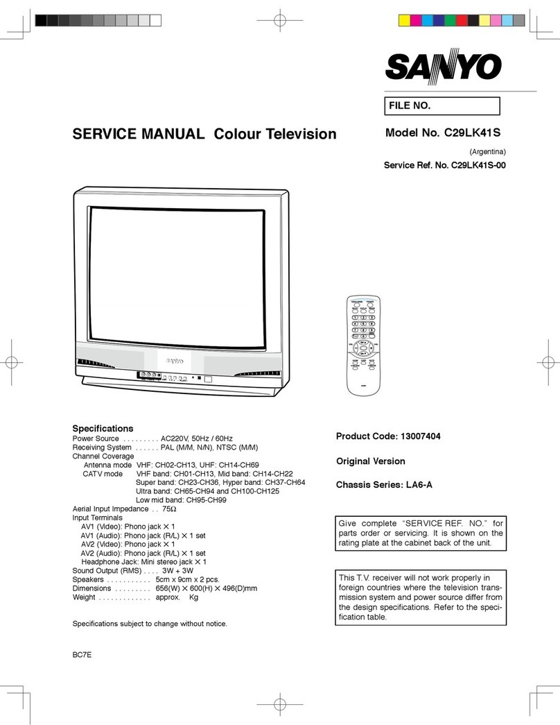
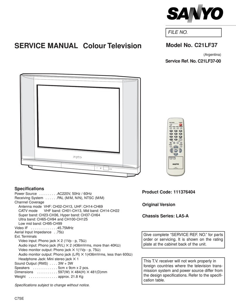
Sanyo HT30746 User manual

AS
FILE NO.
SERVICE MANUAL Remote Control Digital
Color Television HT30746 (U.S.A.)
(CANADA)
ORIGINAL VERSION
Chassis No. 30746-00
NOTE: Match the Chassis No. on
the unit’s back cover with
the Chassis No. in the
Service Manual.
If the Original Version
Service Manual Chassis
No. does not match the
unit’s, additional Service
Literature is required. You
must refer to “Notices” to the
Original Service Manual
prior to servicing the unit.
Contents
Safety Instructions . . . . . . . . . . . . . . . . . . 2
Service Adjustments . . . . . . . . . . . . 3 – 13
Service Hints . . . . . . . . . . . . . . . . . . . . . . 14
Mechanical Disassemblies. . . . . . . . . . . 15
Chassis Electrical Parts List . . . . . . 16 – 32
Cabinet Parts List . . . . . . . . . . . . . . . . . . 33
Component and Test Point
Locations . . . . . . . . . . . . . . . . . . . 34 – 41
Block Diagrams. . . . . . . . . . . . . . . . 42 – 47
Troubleshooting Flow Charts . . . . . 48 – 50
Control Port Function . . . . . . . . . . . 51 – 52
Schematic Inserts . . . . . . . . . . . . . . 53 – 64
Schematic Notes . . . . . . . . . . . . . 53 – 54
Pin Layouts. . . . . . . . . . . . . . . . . . 53 – 54
Capacitor and Resistor Codes . . 53 – 54
Board Connections & Locations. 54 – 56
Waveforms. . . . . . . . . . . . . . . . . . 54 – 56
Main Board. . . . . . . . . . . . . . . . . . 57 – 60
CRT Socket . . . . . . . . . . . . . . . . . 61 – 62
Power and Deflection Board. . . . 61 – 62
Front Board . . . . . . . . . . . . . . . . . 63 – 64
Video Board . . . . . . . . . . . . . . . . . 63 – 64
Specifications
Power Rating . . . . . . . . . . . . . . . . . . . . . 120V, 60Hz
140W (Avg), 2.5A (Max)
Antenna Input Impedance . . . . . . . . . . . . . . . . . 75Ω
UHF/VHF/CATV
Digital
Receiving Channel . . . . . . . . . . . . . . . . 2 - 13 (VHF),
14 - 69 (UHF),
01, 14 - 94, 95 - 125 (CATV)
1 - 99 (Digital)
Remote Ready . . . . . . . . . . 32 Key Remote Control
Sound Output . . . . . . . . . . . . . . . . . . . . . . 5.0 W/CH
Intermediate Frequency
Picture IF Carrier. . . . . . . . . . . . . . . . . . 45.75MHz
Sound IF Carrier . . . . . . . . . . . . . . . . . . 41.25MHz
Color Sub Carrier . . . . . . . . . . . . . . . . . 42.17MHz
Picture Tube . . . . . . . . . . . . . . . . W76QEN693X100
Semiconductors
Integrated Circuits . . . . . . . . . . . . . . . . . . . . . . . 23
Transistors. . . . . . . . . . . . . . . . . . . . . . . . . . . . . 45
Except within Tuners, RC Pre-Amp. & Digital Module
Cabinet Dimensions
Width. . . . . . . . . . . . . . . . . . . . . . . . . . . . . 878 mm
Height . . . . . . . . . . . . . . . . . . . . . . . . . . . . 573 mm
Depth. . . . . . . . . . . . . . . . . . . . . . . . . . . . . 550 mm
REFERENCE No. SM780109
HT30746, H3FLM, PRODUCT CODE 113000990
AS
POWER
CH
VOL
DIGITAL
DOLBY
Servicing should be performed by only trained and qualified service personnel.
with a double “Z” is a registered trademark
of Sanyo Manufacturing Corporation.
© Sanyo Manufacturing Corporation 2006

— 2 —
SAFETY PRECAUTIONS
WARNING: The chassis of this receiver has a floating ground with the
potential of one half the AC line voltage in respect to earth ground.
Service should not be attempted by anyone not familiar with the
precautions necessary when working on this type of equipment.
The following precautions must be observed:
1. An isolation transformer must be connected in the power line
between the receiver and the AC line before any service is
performed on the receiver.
2. Comply with all caution and safety-related notes provided on the
side of the cabinet, inside the cabinet, on the chassis, and the
picture tube.
3. When replacing a chassis in the cabinet, always be certain that all
the protective devices are installed properly, such as control
knobs, adjustment covers, shields and barriers.
4. Before replacing the back cover of the set, thoroughly inspect the
inside of the cabinet to see that no stray parts or tools have been
left inside.
Before returning any television to the customer, the service
technician must perform the following safety checks to be sure
that the unit is completely safe to operate without danger of
electrical shock.
ANTENNA COLD CHECK
Remove AC plug from the 120 VAC outlet and place a jumper
across the two blades. Connect one lead of an ohmmeter to the
jumpered AC plug, and touch the other lead to each exposed antenna
terminal (UHF and VHF antenna terminals). The resistance must
measure between 1M ohm and 5.2M ohm. Any resistance value
below or above this range indicates an abnormality which requires
corrective action.
LEAKAGE CURRENT CHECK
Plug the AC line cord directly into a 120 VAC outlet. (Do not use an
isolation transformer for this check.) Use an AC voltmeter, that has
5000 ohms per volt or more sensitivity. Connect a 1500 ohm 10 watt
resistor, paralleled by a 0.15 µF 150 VAC capacitor, between a
known good earth ground (water pipe, conduit, etc.) and all
exposed metal parts of the cabinet (antennas, handle bracket, metal
cabinet, screw heads, metal overlays, control shafts, etc.). Measure
the AC voltage across the 1500 ohm resistor. The AC voltage should
not exceed 750 mV. A reading exceeding 750 mV indicates that a
dangerous potential exists. The fault must be located and correct-
ed. Repeat the above test with the receiver power plug reversed.
NEVER RETURN A RECEIVER TO THE CUSTOMER WITHOUT
TAKING THE NECESSARY CORRECTIVE ACTION.
PRODUCT SAFETY NOTICE
When replacing components in a receiver, always keep in mind
the necessary product safety precautions. Pay special attention
to the replacement of components marked with a star () in the
parts list and in the schematic diagrams. To ensure safe product
operation, it is necessary to replace those components with the
exact same PARTS.
X-RADIATION PRECAUTION
The primary source of X-RADIATION in solid-state receivers is the pic-
ture tube. The picture tube is specially constructed to limit X-Ray
emission. For continued X-RADIATION protection, the replacement
tube must be the same type as the original (including the suffix letter in
the part numbers). Excessive high voltage may produce potentially
hazardous X-RADIATION. To avoid such hazards, the high voltage must
be maintained within specific limits. Refer to the X-RADIATION WARN-
ING NOTE on the CHASSIS SCHEMATIC in this service manual for
specific high voltage limits. If the high voltage exceeds specified limits,
check the components specified on the chassis schematic diagram
and take the necessary corrective action. Carefully follow the instruc-
tions for the +B Voltage Check and the High Voltage Check to maintain
the high voltage within the specified limits.
HIGH VOLTAGE HOLD-DOWN TEST
To prevent X-RADIATION from the picture tube due to excessive
high voltage, a HOLD-DOWN circuit is provided in the high voltage
circuit. Every time the receiver is serviced, the high voltage HOLD-
DOWN circuit must be tested for proper operation. Refer to the
HIGH VOLTAGE HOLD-DOWN TEST in service adjustments.
SERVICING ELECTROSTATICALLY SENSATIVE DEVICES
Semiconductors (solid-state devices) that can be damaged by static
electricity are referred to as Electrostatically Sensitive (ES) devices.
Examples of typical ES devices are: Integrated Circuits (IC), Field-
Effect Transistors (FET), and “chip” components. The following
techniques should be observed strictly, to reduce the occurrence of
semiconductor damage due to electrostatic discharge.
1. Immediately prior to handling any semiconductor component or
an assembly containing a semiconductor device or devices, dis-
charge the electrostatic buildup on your body by touching a
known earth ground. You may also obtain and wear a commer-
cially available discharging wrist strap device.
CAUTION: Be sure to remove the wrist strap before applying
power to any unit being serviced.
2. After removing an ES equipped assembly, place it on a conduc-
tive surface, such as, aluminum foil, to prevent buildup or
exposure to static electricity.
3. Use only grounded-tip soldering irons to solder or unsolder ES
devices.
4. Use only anti-static solder removal devices. Some suction-type
devices can generate static electricity adequate to damage ES
devices.
5. A replacement ES device will come packaged in protective material
(conductive foam, aluminum foil, or some comparable conductive
material). Do Not remove an ES device from its protective packag-
ing unless you are prepared to install it immediately.
6. Precisely prior to removing an ES device from its protective pack-
aging, touch the protective packaging to the chassis or
assembly in which the device will be installed.
CAUTION: Be sure that no power is applied to the chassis or circuit
assembly.
7. Incidental body movements, such as, lifting a foot from a carpeted
floor or the rubbing of fabric together can generate static electricity
sufficient to damage ES devices. Therefore, minimize all body
movements while handling exposed (unpackaged) ES devices.
SAFETY INSTRUCTIONS
0.15 µF 150V AC
1500 ohm
10 watt
Good earth ground
such as a water pipe,
conduit, etc.
AC OUTLET
TELEVISION
RECEIVER
READING SHOULD NOT EXCEED 750 mV.
AC VOLTMETER
(5000 ohms per volt or more sensitivity)
To be touched to all of exposed metal parts.
Voltmeter Hook-up for Leakage Current Check.

GENERAL
This set has an On-screen Service Menu system included in the CPU that allows remote operation for most of the service adjustments.
ON-SCREEN SERVICE MENU SYSTEM
1. Enter the Service Menu:
•While pressing the VOLUME – key on the front control panel,
reconnect the AC power cord. The Service Menu Display will now
appear. The remote can now be used to make adjustments.
See Figure 1.
2. Service Adjustments:
•Press the Channel or key to select the desired service
menu you want to adjust. See page 5 for On-screen Service
Menu.
•Use the Volume + or – key or numeric keys to adjust the data.
(For Sub - Address see below)
3. Exit from the Service Menu:
•Press the MENU key to turn off the Service Menu display.
ADJUSTMENT FOR SUB ITEM (ADDRESS)
Some service data have Sub - Addresses. Use the numeric keys (from 0 to 7), to adjust the Sub - item data.
ADJUST DATA OF SUB-TITLE
1. Find the title and its bit of binary data from Table 1 (On-Screen Service Menu).
2. Enter the service menu (see above) and select the item number needed with the Channel or key.
3. With the numeric key (from 0 to 7), change the bit data. Each time the numeric key is pressed, the data changes
from 0 to 1 alternately. For example, to change the data of bit 5, press the “5” key.
NOTE: The and symbols used in the following service adjustments refer to the Channel Up and Down keys not the
Menu keys.
SERVICE ADJUSTMENTS
— 3 —
XXX XXXX
XXX XXXXX
XX XXXXXXXX
Figure 1. Service Menu Display
ITEM NO. TITLE
BINARY DATA
(8 bit)
HEXADECIMAL
DATA
(b7) (b6) (b5) (b4) (b3) (b2) (b1) (b0)
0 1 0 1 0 1 1 0 BINARY DATA
(8 bit)
IC802 (EEPROM) REPLACEMENT
When IC802 (EEPROM) is replaced, IC801 (CPU) will automatically write the initial reference data into IC802 for basic TV operation.
However, the bus data should be checked and some bus data should be set up before attempting the service adjustments.
(See Table 1. on pages 5 – 13 for detailed bus data information.)
INITIAL BUS DATA SETUP
Note: When IC802 (EEPROM) is replaced, change the following initial reference data for proper TV operation before
attempting service adjustments.
1. Disconnect the AC power cord (AC 120V line).
2. While pressing the Volume – key, reconnect the AC power cord. The Service Menu display will now appear.
3. Select NO. 103 SHU2PO (Sub Hue / Pre/Over Shoot) with or key. Adjust the data with number keys for 3F.
4. Select NO. 104 SLC2CTI (Sub Color / CTI Level) with or key. Adjust the data with number keys for 31.
5. Select NO. 106 SSH2LTI (Sub Sharp / LTI Level) with or key. Adjust the data with number keys for A3.
6. Select NO. 10A SBR2GAM (Sub Bright / Gamma) with or key. Adjust the data with number keys for 4F.
7. Select NO. 10B RCT2LTIM1 (R Cutoff / LTI Mode) with or key. Adjust the data with number keys for 56.
8. Select NO. 10D BCT2DCT (B Cutoff / DC Tran) with or key. Adjust the data with number keys for 53.
9. Select NO. 110 CBOF2AW1AB (CB Offset / Aging W / Aging B) with or key. Adjust the data with number
keys for 48.
CPU VERSION

— 4 —
SERVICE ADJUSTMENTS (Cont.)
INITIAL BUS DATA SETUP (Cont.)
10. Select NO. 111 CROF2SYS (CR Offset / System ) with or key. Adjust the data with number keys for 48.
11. Select NO. 113 RYR4RYB (R-Y/R / R-Y/B ) with or key. Adjust the data with number keys for 88.
12. Select NO. 114 GYR4GYB (G-Y/R / G-Y/B with or key. Adjust the data with number keys for 88.
13. Select NO. 117 VS (V Size) with or key. Adjust the data with number keys for 62.
14. Select NO. 118 VPS (V Position) with or key. Adjust the data with number keys for 74.
15. Select NO. 119 VLI4SCR (V Lin / S Correction) with or key. Adjust the data with number keys for 73.
16. Select NO. 11B PAP2LUP (Pin Amp / Lo UCP) with or key. Adjust the data with number keys for 5C.
17. Select NO. 11C UCP 2UUG (Up CPin / Up UCG) with or key. Adjust the data with number keys for 74.
18. Select NO. 11D LCP2LUG (Up CPin / Lo UCG) with or key. Adjust the data with number keys 7C.
19. Select NO. 11E PPH2UPO1VBS (Pin Phase / Uc Pol / V Blk Sw) with or key. Adjust the data with
number keys 65.
20. Select NO. 11F HPO2CSH1NIN (H Position / CLP Shift / Non Inter) with or key. Adjust the data with
number keys for B5.
21. Select NO. 120 ABO2RAM (AFC Bow / RF AFC Mode) with or key. Adjust the data with number keys for 79.
22. Select NO. 121 AAN2AGS1 (AFC Angle / AFC Switch) with or key. Adjust the data with number keys for 70.
23. Select NO. 127 VCP4HCP (V Comp / H Comp) with or key. Adjust the data with number keys for 96.
24. Select NO. 12C 4I-COL (Component 2,3 / 480I Color) with or key. Adjust the data with number keys for 06.
25. Select NO. 12D 4P-COL (Component 2,3 / 480P Color) with or key. Adjust the data with number keys for 06.
26. Select NO. 12E 1I-COL (Component 2,3 / 1080I/720P Color) with or key. Adjust the data with
number keys for 06.
27. Select NO. 12F H-COL (HDMI Color) with or key. Adjust the data with number keys for 06.
28. Select NO. 130 D-COL (Digital Color) with or key. Adjust the data with number keys for 06.
29. Select NO. 14A RF-VMF (NTSC(RF) / VM DLY) with or key. Adjust the data with number keys for 00.
30. Select NO. 14B 4I-VMF (Component 2,3 / 480I VM FO) with or key. Adjust the data with number
keys for 00.
31. Select NO. 14C 4P-VMF (Component 2,3 / 480P VM FO) with or key. Adjust the data with number
keys for 00.
32. Select NO. 14D 1I-VMF (Component 2,3 / 1080I/720P VM FO) with or key. Adjust the data with number
keys for 00.
33. Select NO. 14E H-VMF (HDMI VM FO) with or key. Adjust the data with number keys for 00.
34. Select NO. 14F D-VMF (Digital VM FO) with or key. Adjust the data with number keys for 00.
35. Select NO. 160 4IHPO (Component 2,3 / 480I Full H Position) with or key. Adjust the data with number
keys for FA.
36. Select NO. 16C 4PHPO (Component 2,3 / 480P Full H Position) with or key. Adjust the data with number
keys for FA.
37. Select NO. 179 4PHPO (Component 2,3 / 720P Full H Position) with or key. Adjust the data with number
keys for FA.
38. Select NO. 185 1IHPO (Component 2,3 / 1080IP Full H Position) with or key. Adjust the data with number
keys for FA.
39. Select NO. 191 DHPO (Digital/HDMI Full H Position) with or key. Adjust the data with number keys for FA.
40. Select NO. 089 OSD (OSD H Position) with or key. Adjust the data with number keys for 0F.
41. Press the MENU key to turn off the Service Menu display.

— 5 —
Table 1. ON-SCREEN SERVICE MENU
When IC802 (EEPROM) is replaced, check the bus data to confirm they are the same as below. The shaded menu should be
checked and be set up or readjusted according to the procedures described in the following pages. Initial Setup Data marked
with an * should be changed from Initial Reference Data. (See pages 3 and 4 for Initial Bus Data Setup.)
No. TITLE INITIAL REFERENCE INITIAL SETUP INITIAL SETUP FUNCTION
DATA HEX DATA HEX DATA BINARY
101 RGBON4DL2SF FD FD 11111101 PIC+R+G+B On(7~4), D COL(3~2), ES1(1):0(fixed), SF(0)
102 BLKBTM 00 00 00000000 BLK_BTM(1~0)
103 SHU2PO 23 3F* 00111111 SUB HUE(7~2), PRE/OVER(1~0)
104 SCL2CTI 11 31* 0011001 SUB COLOR(7~2), CTI_LEV(1~0)
105 ↓↓↓↓NOT USED
106 SSH2LTI 89 A3* 10100011 SUB SHARPNESS(7~2), LTI_LEV(1~0)
107 RD2PTL 7C 7C 01111100 R_DRIVE(7~2), PLIMIT_LEV(1~0)
108 GD2ABLM 7F 7F 01111111 G_DRIVE(7~2), ABL_MODE(1~0)
109 BD2CTIM1 7C 7C 01111100 B_DRIVE(7~2), CTI_MODE(1)
10A SBR2GAM 29 4F* 01001111 SUB_BRIGHT(7~2), GAMMA(1~0)
10B RCT2LTIM1 58 56* 01010110 R_CUTOFF(7~2), LTI_MODE(1)
10C GCT2DPL 1D 1D 00011101 G_CUTOFF(7~2), DPIC_LEV(1~0)
10D BCT2DCT 35 53* 01010011 B_CUTOFF(7~2), DC_TRAN(1~0)
10E SCO4LR2L 57 57 01010111 SUB_CONT(7~4), LRGB2_LEV(3~0)
10F PABL4ABLT F1 F1 11110001 P_ABL(7~4), ABL_TH(3~0)
110 CB0F2AW1AB 94 48* 01001000 CB_OFFSET(7~2), AGING_W(1), AGING_B(0)
111 CROF2SYS B8 48* 01001000 CR_OFFSET(7~2), SYSTEM(1~0)
112 YOF4VD2VF 02 02 00000010 Y_OFFSET(7~4), VM_DLY(3~2), VM_FO(1~0)
113 RYR4RYB 8C 88* 10001000 R-Y/R(7~4), R-Y/B(3~0)
114 GYR4GYP 84 88* 10001000 G-Y/R(7~4),G-Y/B(3~0)
115 VML4FLC2FLS F0 F0 11110000 VM_LEV(7~4), FLCOL(3~2), FLCOL SW(1)
116 UBK4LBK 00 00 00000000 UP_BLK(7~4), LO_ BLK(3~0)
117 VS 72 62* 01100010 V_SIZE(7~2), bit1:1 bit0:0 (b1/b0: fixed)
118 VPS 64 74* 01110100 V_POSITION(7~2)
119 VLI4SCR 63 73* 01110011 V_LIN(7~4), S_CORRECTION(3~0)
11A HSI2UUC 70 70 01110000 H_SIZE(7~2), UP_UCP(1~0)
11B PAP2LUP 94 5C* 01011100 PIN AMP(7~2), LO UCP(1~0)
11C UCP2UUG 9C 74* 01110100 UP_CPIN(7-2), UP_UCG(1-0)Y
11D LCP2LUG A8 7C* 01111100 LO_CPIN(7~2), LO_UCG(1-0)
11E PPH2UPO1VBS 55 65* 01100101 PIN_PHASE(7~2), UC_POL(1), VBLK_SW(0)
11F HPO2CSH1NIN 95 B5* 10110101 H_POSITION(7~2), CLP_SHIFT(1),NON INTER(0)
120 ABO2RAM 81 79* 01111001 AFC_BOW(7~2), RF AFC_MODE(1-0)
121 AAN2AGS1 7C 70* 01110000 AFC_ANGLE(7~2), AGC_SW(1)
122 LBK2CPH BC BC 10111100 LEFT_BLK(7-2), CLP_PHASE(1~0)
123 RBK2CGA1HSW 9D 9D 10011101 RIGHT_BLK(7-2), CLP_GATE(1), HBLK_SW(0)
124 VAS2ZSW1JSW 00 00 00000000 V_ASPECT(7~2), Z_SW(1), JMP_SW(0)
125 VSR 7D 7D 01111101 V_SCROLL(7~2), b1 : 0, b0 : 1 (b1 / b0: fixed)
126 UVL4LVL 00 00 00000000 UP_VLIN(7~4), LO_VLIN(3~0)
127 VCP4HCP 76 96* 10010110 V_COMP(7~4), H_COMP(3~0)
128 ATI3HVS2BOF1AOF 70 70 01110000 AKB-TIM(7~3), HVBTM_SW(2),BLK OFF(1), AKB OFF(0)
129 W-CON 00 00 00000000 LETTER BOX CONTRAST
12A RF-PRE 02 02 00000010 NTSC(RF) PRE/OVER(1~0)
12B RF-COL 00 00 00000000 NTSC(RF) COLOR
12C 4I-COL 00 06* 00000110 COMPONENT2,3, 480I COLOR
12D 4P-COL 00 06* 00000110 COMPONENT2,3, 480P COLOR
12E 1I-COL 00 06* 00000110 COMPONENT2,3 1080I/720P COLOR
12F H-COL 00 06* 00000110 HDMI COLOR
130 D-COL 00 06* 00000110 DIGITAL COLOR
131 RF-CB 00 00 00000000 NTSC(RF) CB_OFFSET
132 4I-CB 00 00 00000000 COMPONENT2, 3 480I CB_OFFSET

Table 1. ON-SCREEN SERVICE MENU (Continued)
— 6 —
SERVICE ADJUSTMENTS (Cont.)
No. TITLE INITIAL REFERENCE INITIAL SETUP INITIAL SETUP FUNCTION
DATA HEX DATA HEX DATA BINARY
133 4P-CB 00 00 00000000 COMPONENT2,3 480P CB_OFFSET
134 1I-CB 00 00 00000000 COMPONENT2,3 1080I/720P CB-OFFSET
135 H-CB 00 00 00000000 HDMI CB_OFFSET
136 D-CB 00 00 00000000 DIGITAL CB_OFFSET
137 RF-CR 00 00 00000000 NTSC(RF) CR_OFFSET
138 4I-CR 00 00 00000000 COMPONENT2,3 480I CR_OFFSET
139 4P-CR 00 00 00000000 COMPONENT2,3 480P CR_OFFSET
13A 1I-CR 00 00 00000000 COMPONENT2,3 1080I/720P CR_OFFSET
13B H-CR 00 00 00000000 HDMI CR_OFFSET
13C D-CR 00 00 00000000 DIGITAL CR_OFFSET
13D W-CR 00 00 00000000 LETTER BOX CR_OFFSET
13E RF-SYS 00 00 00000000 NTSC(RF) SYSTEM(1~0)
13F 4I-SYS 00 00 00000000 COMPONENT2,3 480I SYSTEM(1~0)
140 4P-SYS 00 00 00000000 COMPONENT2,3 480P SYSTEM(1~0)
141 1I-SYS 01 01 00000001 COMPONENT2,3 1080I/720P SYSTEM(1~0)
142 H-SYS 01 01 00000001 HDMI SYSTEM(1~0)
143 D-SYS 01 01 00000001 DIGITAL SYSTEM(1~0)
144 RF-VMD 00 00 00000000 NTSC(RF) VM_DLY(1~0)
145 4I-VMD 00 00 00000000 COMPONENT2,3 480I VM_DLY(1~0)
146 4P-VMD 00 00 00000000 COMPONENT2,3 480P VM_DLY(1~0)
147 1I-VMD 00 00 00000000 COMPONENT2,3 1080I/720P VM_DLY(1~0)
148 H-VMD 00 00 00000000 HDMI VM_DLY(1~0)
149 D-VMD 00 00 00000000 DIGITAL VM_DLY(1~0)
14A RF-VMF 02 00* 00000000 NTSC(RF) VM_F0(1~0)
14B 4I-VMF 02 00* 00000000 COMPONENT2,3 480I VM_F0(1~0)
14C 4P-VMF 02 00* 00000000 COMPONENT2,3 480P VM_F0(1~0)
14D 1I-VMF 02 00* 00000000 COMPONENT2,3 1080I/720P VM_F0(1~0)
14E H-VMF 02 00* 00000000 HDMI VM_F0(1~0)
14F D-VMF 02 00* 00000000 DIGITAL VM_F0 (1~0)
150 CFVS 00 00 00000001 VIDEO1 FULL V_SIZE
151 CFVPS 00 00 00000000 VIDEO1 FULL V_POSITION
152 CFHSI 00 00 00000000 VIDEO1 FULL H_SIZE
153 CFHPO 00 00 00000000 VIDEO1 FULL H_POSITION
154 CWUBK 08 08 00001000 VIDEO1 LETTER BOX UP_BLK
155 CWLBK 0B 0B 00000000 VIDEO1 LETTER BOX LO_BLK
156 CWVS 00 00 00000000 VIDEO1 LETTER BOX V_SIZE
157 CWVPS 00 00 00000000 VIDEO1 LETTER BOX V_POSITION
158 CWVBS 01 01 00000001 VIDEO1 LETTER BOX VBLK_SW(0)
159 CWVAS 12 12 00010020 VIDEO1 LETTER BOX V_ASPECT
15A CWJSW 01 01 00000001 VIDEO1 LETTER BOX JMP_SW(0)
15B CWVSR 00 00 00000000 VIDEO1 LETTER BOX V_SCROLL
15C 15C 00 00 00000000 VIDEO1 PRELIMINARY
15D 4IVS 00 00 00000000 COMPONENT2,3 480I FULL V_SIZE
15E 4IVPS 00 00 00000000 COMPONENT2,3 480I FULL V_POSITION
15F 4IHSI 00 00 00000000 COMPONENT2,3 480I FULL H_SIZE
160 4IHPO 00 FA* 11111010 COMPONENT2,3 480I FULL H_POSITION
161 4IWUBK 08 08 00001000 COMPONENT2,3 480I LETTER BOX UP_BLK
162 4IWLBK 0B 0B 00001010 COMPONENT2,3 480I LETTER BOX LO_BLK
163 4IWVS 00 00 00000000 COMPONENT2,3 480I LETTER BOX V_SIZE
164 41WVPS 00 00 00000000 COMPONENT2,3 480I LETTER BOX V_POSITION

— 7 —
No. TITLE INITIAL REFERENCE INITIAL SETUP INITIAL SETUP FUNCTION
DATA HEX DATA HEX DATA BINARY
165 4IWVBS 01 01 00000001 COMPONENT2,3 480I LETTER BOX VBLK_SW(0)
166 4IWVAS 12 12 00010010 COMPONENT2,3 480I LETTER BOX V_ASPECT
167 4IWJSW 01 01 00000001 COMPONENT2,3 480I LETTER BOX JMP_SW(0)
168 4IWVSR 00 00 00000000 COMPONENT2,3 480I LETTER BOX V_SCROLL
169 4PVS 00 00 00000000 COMPONENT2,3 480P FULL V_SIZE
16A 4PVPS 00 00 00000000 COMPONENT2,3 480P FULL V_POSITION
16B 4PHSI 00 00 00000000 COMPONENT2,3 480P FULL H_SIZE
16C 4PHPO 00 FA* 11111010 COMPONENT2,3 480P FULL H_POSITION
16D 4PWUBK 08 08 00001000 COMPONENT2,3 480P LETTER BOX UP_BLK
16E 4PWLBK 0B 0B 00001011 COMPONENT2,3 480P LETTER BOX LO_BLK
16F 4PWVS 00 00 00000000 COMPONENT2,3 480P LETTER BOX V_SIZE
170 4PWVPS 00 00 00000000 COMPONENT2,3 480P LETTER BOX V_POSITION
171 4PWVBS 01 01 00000001 COMPONENT2,3 480P LETTER BOX VBLK_SW(0)
172 4PWVAS 12 12 00010010 COMPONENT2,3 480P LETTER BOX V_ASPECT
173 4PWJSW 01 01 00000001 COMPONENT2,3 480P LETTER BOX JMP_SW(0)
174 4PWVSR 00 00 00000000 COMPONENT2,3 480P LETTER BOX V_SCROLL
175 175 00 00 00000000 COMPONENT2,3 480P PRELIMINARY
176 7PVS 00 00 00000000 COMPONENT2,3 720P FULL V_SIZE
177 7PVPS 00 00 00000000 COMPONENT2,3 720P FULL V_POSITION
178 7PHSI 00 00 00000000 COMPONENT2,3 720P FULL H_SIZE
179 7PHPO 00 FA* 11111010 COMPONENT2,3 720P FULL H_POSITION
17A 7PWUBK 08 08 00001000 COMPONENT2,3 720P LETTER BOX UP_BLK
17B 7PWLBK 0B 0B 00001011 COMPONENT2,3 720P LETTER BOX LO_BLK
17C 7PWVS 00 00 00000000 COMPONENT2,3 720P LETTER BOX V_SIZE
17D 7PWVPS 00 00 00000000 COMPONENT2,3 720P LETTER BOX V_POSITION
17E 7PWVBS 01 01 00000001 COMPONENT2,3 720P LETTER BOX VBLK_SW(0)
17F 7PWVAS 12 12 00010010 COMPONENT2,3 720P LETTER BOX V_ASPECT
180 7PWJSW 01 01 00000001 COMPONENT2,3 720P LETTER BOX JMP_SW(0)
181 7PWVSR 00 00 00000000 COMPONENT2,3 720P LETTER BOX V_SCROLL
182 1IVS 00 00 00000000 COMPONENT2,3 1080I FULL V_SIZE
183 1IVPS 00 00 00000000 COMPONENT2,3 1080I FULL V_POSITION
184 1IHSI 00 00 00000000 COMPONENT2,3 1080I FULL H_SIZE
185 1IHPO 00 FA* 11111010 COMPONENT2,3 1080I FULL H_POSITION
186 1IWUBK 08 08 00001000 COMPONENT2,3 1080I LETTER BOX UP_BLK
187 1IWLBK 0B 0B 00001011 COMPONENT2,3 1080I LETTER BOX LO_BLK
188 1IWVS 00 00 00000000 COMPONENT2,3 1080I LETTER BOX V_SIZE
189 1IWVPS 00 00 00000000 COMPONENT2,3 1080I LETTER BOX V_POSITION
18A 1IWVBS 01 01 00000001 COMPONENT2,3 1080I LETTER BOX VBLK_SW(0)
18B 1IWVAS 12 12 00010010 COMPONENT2,3 1080I LETTER BOX V_ASPECT
18C 1IWJSW 01 01 00000001 COMPONENT2,3 1080I LETTER BOX JMP_SW(0)
18D 1IWVSR 00 00 00000000 COMPONENT2,3 1080I LETTER BOX V_SCROLL
18E DVS 00 00 00000000 DIGITAL/HDMI FULL V_SIZE
18F DVPS 00 00 00000000 DIGITAL/HDMI FULL V_POSITION
190 DHSI 00 00 00000000 DIGITAL/HDMI FULL H_SIZE
191 DHPO 00 FA* 11111010 DIGITAL/HDMI FULL H_POSITION
192 RZVSR 00 00 00000000 NTSC(RF) V_SCROLL
193 CZVSR 00 00 00000000 VIDEO1 V_SCROLL
194 4IZVSR 00 00 00000000 COMPONENT2,3 480I V_SCROLL
195 4PZVSR 00 00 00000000 COMPONENT2,3 480P V_SCROLL
196 7PZVSR 00 00 00000000 COMPONENT2,3 720P V_SCROLL
197 1IZVSR 00 00 00000000 COMPONENT2,3 1080I V_SCROLL
198 DZVSR 00 00 00000000 DIGITAL/HDMI V_SCROLL
199 DWUBK 08 08 00001000 DIGITAL/HDMI LETTER BOX UP_BLK
19A DWLBK 0B 0B 00001011 DIGITAL/HDMI LETTER BOX LO_BLK

— 8 —
SERVICE ADJUSTMENTS (Cont.)
Table 1. ON-SCREEN SERVICE MENU (Continued)
No. TITLE INITIAL REFERENCE INITIAL SETUP INITIAL SETUP FUNCTION
DATA HEX DATA HEX DATA BINARY
19B DWVS 00 00 00000000 DIGITAL/HDMI LETTER BOX V_SIZE
19C DWVPS 00 00 00000000 DIGITAL/HDMI LETTER BOX V_POSITION
19D DWVBS 01 01 00000001 DIGITAL/HDMI LETTER BOX VBLK_SW(0)
19E DWVAS 12 12 00010020 DIGITAL/HDMI LETTER BOX V_ASPECT
19F DWJSW 01 01 00000001 DIGITAL/HDMI LETTER BOX JMP_SW(0)
1A0 DWVSR 00 00 00000000 DIGITAL/HDMI LETTER BOX V_SCROLL
1A1 VMUTE 00 00 00000000 NOT AVAILABLE
1A2 VMUTE2 00 00 00000000 NOT AVAILABLE
201 1R00 00 00 00000000 ROM CORRECTION DATA AREA
↓↓ ↓ ↓ ↓↓
298 2R48 00 00 00000000 ROM CORRECTION DATA AREA
080 ATT 07 07 00000111 MTS INPUT LEVEL(3~0)
081 SPC 20 20 00010000 MTS HIGH SEPARATION(5~0)
082 WDB 20 20 00010000 MTS LOW SEPARATION(5~0)
083 SCO 00 00 00000000 NOT AVAILABLE
084 STI 00 00 00000000 NOT AVAILABLE
085 SBR 00 00 00000000 NOT AVAILABLE
086 SSH 00 00 00000000 NOT AVAILABLE
087 OP1 08 08 00001000 OPTION 1 DATA (b3: WO/HDMI=1, W/HDMI=0)
088 OP2 02 02 00000000 OPTION 2 DATA (b1: ASPECT 16:9=1, 4:3=0)
089 OSD 02 0F* 00001111 OSD H-POSITION
08A 08A 00 00 00000000 NOT AVAILABLE
08B VMT C0 C0 00000000 VIDEO MUTE TIME
08C AKB 10 10 00010000 AKB DETECT TIME
08D HS12 00 00 00000000 NOT AVAILABLE
08E HPO 00 00 00000000 NOT AVAILABLE
–R/B DRIVE – – – R / B DRIVE LEVEL ADJUSTMENT
–SCREEN – – – BLACK SCREEN FOR SCREEN ADJUSTMENT

— 9 —
PROGRAM CODES
The microprossesor used in this model is a multi-purpose
type and is used in several different models. To ensure
proper operation and the correct features for your particu-
lar model, the program codes must be correct.
Note 1. Option Data 1 (NO. 087 OP1) should be
Hexadecimal 08 (00001000 binary). If this program code is
wrong the TV will not operate properly.
Note 2. Option Data 2 (NO. 088 OP2) should be
Hexadecimal 02 (00000010 binary). If this program code is
wrong the TV will not operate properly.
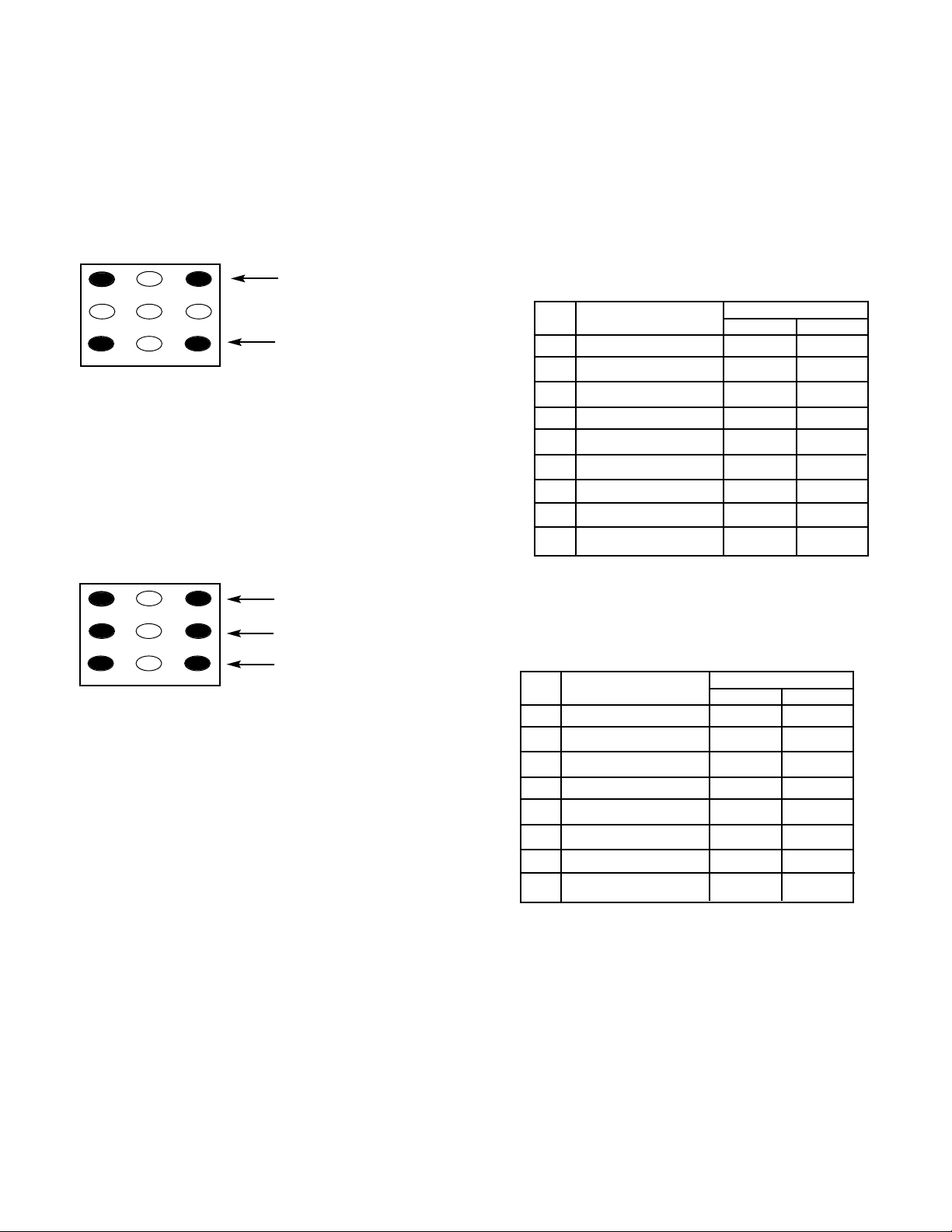
BIT FUNCTION DATA
01
0NOT USED – –
1TV ASPECT RATIO 4:3 16:9
2NOT USED – –
3NOT USED – –
4NOT USED – –
5NOT USED – –
6NOT USED – –
7NOT USED – –
BIT FUNCTION DATA
01
0~! HDTV 0 0 –
0~1 LCD 0 1
0~1 PDP 1 0
2NOT USED – –
3HDMI NO YES
4LCD SIZE 32”– 26”–
5NOT USED – –
6NOT USED – –
7PDP RESOLUTION HD ED
Note 1.
Red/Blue Drive Adjustments in Service Menu NO. 08F RB
DRV: Adjust Red and Blue Drive Levels alternately with 1, 3,
7, and 9 keys on the remote control. See Figure 2. The Drive
Level adjustment data will be written in the Service Menu
No. 107 RD and 109 BD automatically.
123
456
7 98
RB(–) RB(+)
BB(–) BB(+)
(N/A)
GB(–) (N/A) GB(+)
(N/A)
FOR RED BIAS ADJUSTMENT
FOR BLUE BIAS ADJUSTMENT
FOR GREEN BIAS ADJUSTMENT
Figure 2.
Figure 3.
123
4 5 6
7 98
RD(–) RD(+)
BD(–) BD(+)
(N/A)
(N/A) (N/A) (N/A)
(N/A)
FOR RED DRIVE ADJUSTMENT
FOR BLUE DRIVE ADJUSTMENT
Note 2.
Red/Green/Blue Bias Adjustments in Service Menu
SERVICE 090 (Black Screen):
Adjust each Bias Level with 1, 3, 4, 6, 7, or 9 key on the
remote control. See Figure 3. The Bias Level adjustment
data will be written in the Service Menu No. 10B RC,
No. 10C GC, and No. 10D BC automatically.
DRIVE AND BIAS ADJUSTMENTS

— 10 —
SERVICE ADJUSTMENTS (Continued)
ANTENNA CONNECTIONS
This receiver is designed for UHF/VHF and Digital RF recep-
tion. A 75 ohm terminal is provided for UHF/VHF reception
and a separate 75 ohm terminal is provided for Digital RF
reception. When connecting a CATV antenna system, con-
nect the 75 ohm coaxial cable directly to the 75 ohm
terminal. For 300 ohm VHF antenna, use an adapter (not
included with the TV set).
CIRCUIT PROTECTION
Fuse F601 (6A) is included in the AC line. This fuse must be
replaced with the proper fuse (see Parts List).
+B VOLTAGE CHECK
1. Connect Voltmeter + lead to TJ1 (140.5 V) and – lead to
ground (Power/Deflection board).
2. Connect receiver to AC 120V line.
3. Tune receiver to an active channel.
4. Set the picture controls to the Auto level or Reset (use
MENU key and or key or RESET key).
5. Voltage must measure between 139.0 V and 142.0V.
If the voltage is out of range, the power circuit must be
checked. No +B adjustment is provided on this chassis.
HORIZONTAL CENTERING ADJUSTMENT
1. Tune receiver to an active channel.
2. Check that picture is in the horizontal center of TV
screen. If picture is not centered horizontally, perform
steps 3 - 6.
3. Turn off the receiver and disconnect the AC power cord.
(120V AC line)
4. While pressing the VOLUME – key, reconnect the AC
power cord. The Service Menu display will now appear.
5. Select NO. 11F (HPO2: Horizontal Position, Bit 7 - 2) with
or key.
6. Adjust the data with numeric keys for horizontal center. To
turn off the Service Menu display, press the MENU key.
HORIZONTAL WIDTH ADJUSTMENT
1. Tune receiver to an active channel.
2. Check the picture for proper width. If width is not cor-
rect, perform steps 3 - 6.
3. Turn off the receiver and disconnect the AC power cord.
4. While pressing the VOLUME – key, reconnect the AC
power cord. The Service Menu display will now appear.
5. Select NO. 11A (HSI2: Horizontal Size, Bit 7 - 2) with
or key.
6. Adjust the data with numeric keys for proper width. To
turn off the Service Menu display, press the MENU key.
VERTICAL SIZE ADJUSTMENT
1. Tune receiver to an active analog channel.
2. Check the vertical size of the picture. If the vertical size
is too large or small, perform steps 3 ~ 6.
3. Turn off the receiver and disconnect the AC power cord.
4. While pressing the VOLUME – key, reconnect the AC
power cord. The Service Menu display will now appear.
5. Select NO. 117 (VS: Vertical Size, Bit 7 - 2) with or
key.
6. Adjust the data with + or – key for full scan. To turn off
the Service Menu display, press the MENU key.
VERTICAL CENTERING ADJUSTMENT
1. Tune receiver to an active analog channel.
2. Check that picture is in the vertical center of TV screen.
If picture is not centered vertically, perform steps 3 - 6.
3. Turn off the receiver and disconnect the AC power cord.
4. While pressing the VOLUME – key, reconnect the AC
power cord. The Service Menu display will now appear.
5. Select NO. 118 (VPS: Vertical Position) with or key.
6. Adjust the data with numeric key for vertical center. To
turn off the Service Menu display, press the MENU key.
GRAYSCALE ADJUSTMENT
1. Connect a color-bar generator to the analog antenna
terminal.
2. Switch the generator to the white pattern.
3. Set the picture controls to the AUTO level or Reset (use
MENU key and or key or RESET key).
4. Turn off the receiver and disconnect the AC power cord
(120V AC line).
5. While pressing the VOLUME – key, reconnect the AC
power cord. The Service Menu display will now appear.
6. Select the following service menu items with the or
keys and set the data with the numeric keys.
7. Select NO. 107 RD2 (Red Drive) and set data to 7C, NO. 108
GD2 (Green Drive) and set data to 7F, and NO. 109 BD2
(Blue Drive) and set data to 7C.
8. Set NO. 10B RCT2 (Red Cutoff) data to 56, NO. 10C GCT2
(Green Cutoff) data to 1D, and NO. 10D BCT2 (Blue Cutoff)
data to 53.
9. Set NO. 10A SBR2 (Sub Brightness) data to 4F and
NO. 106 SSH2 (Sub Sharpness) data to A3.
Screen Adjustment
10. Connect oscilloscope probe (at least 50:1) to TP47G and
ground lead to TE47 on the CRT socket PWB.
11. Select “Screen Adjustment” Menu NO. 090 with or
key (Black Picture).
12. Adjust Screen Control (T402) to obtain 15 Vp-p from
black to white level. (See Figure 2.)
CAUTION FOR CONTINUED PROTECTION AGAINST
A RISK OF FIRE, REPLACE ONLY WITH THE
SAME TYPE 6A, 125V FUSE.
ATTENTION : POUR MAINTENIR LA PRO-
TECTION CONTRE LES RISQUES
D’ INCENDIE UTILISER UN FUSIBLE DE
RECHANGE DE MEME TYPE 6A, 125V.
6A 125V
1V
15 Vp-p
Figure 2.

— 11 —
Drive Level Adjustment
13. Select “Drive Level Adjustment” Menu NO. 08F with
or key. The Menu display will appear.
14. Adjust Red and Blue Drive Levels alternately with 1, 3,
7, or 9 key to produce normal black and white picture in
highlight areas. The Drive Level adjustment data will be
written in the Service Menu No. 107 and 109 automati-
cally. (See Figure 3.)
15. Check for proper grayscale at all brightness levels.
Note: If Grayscale Adjustment is made after picture tube
replacement, check Brightness Adjustment.
BRIGHTNESS LEVEL ADJUSTMENT
Note: Grayscale Adjustment and High Voltage Check must be
completed before attempting Brightness Level
Adjustment.
1. Connect a color-bar generator to the analog antenna
terminal.
2. Switch the generator to the 15 IRE flat pattern.
3. Reset the picture controls to the AUTO level. PIX2 mode.
4. Connect voltmeter (high impedance) + lead to terminal
TP51 and – lead to terminal TP50 on P/D board. Set
voltmeter for 1.5V ~ 3V range.
5. Turn off the receiver and disconnect the AC power cord.
6. While pressing the VOLUME – key, reconnect the AC
power cord. The Service Menu display will now appear.
7. Select NO. 10A (SBR2: Sub Brightness, Bit 7 - 2) with
or key.
8. Adjust the data with numeric keys for 20mVDC± .05.
9. Press the MENU key to turn off the Service Menu display.
10. Check brightness level on every active channel, readjust
(repeat steps 5 ~ 9), if necessary.
Note: Do not set to excessive brightness level, otherwise
the contrast level will be suppressed.
SUB CONTRAST ADJUSTMENT
1. Connect a color-bar generator to the analog antenna
terminal.
2. Switch the generator to the crosshatch pattern.
3. Connect oscilloscope probe (at least 50:1) to TP47G and
ground lead to TE47 on the CRT socket PWB.
4. Turn off the receiver and disconnect the AC power cord.
5. While pressing the VOLUME – key, reconnect the AC
power cord. The Service Menu display will now appear.
6. Select NO. 10A (SBR2: Sub Brightness, Bit 7 - 2) with
or key. Remember this data setting.
7. Set the data with numeric key to 2E with numeric keys.
8. Select NO. 10E (SCO4: Sub Contrast, Bit 7 - 4) with
or key.
9. Set the data with numeric keys 4 - 7 for 100Vp-p.
10. Reset brightness level to previous data (repeat steps
6 – 7). To turn off the Service Menu display, press the
MENU key.
SUB COLOR AND SUB HUE ADJUSTMENT
Sub Hue (Tint)
1. Connect a color-bar generator to the analog antenna
terminal. Set picture controls to Auto level.
2. Switch the generator to the color-bar (NTSC) pattern.
3. Connect oscilloscope probe (at least 50:1) to TP47G and
ground lead to TE47 on the CRT socket PWB.
4. Turn off the receiver and disconnect the AC power cord.
5. While pressing the VOLUME – key, reconnect the AC
power cord. The Service Menu display will now appear.
6. Select NO. 103 (SHU2: Sub HUE, Bit 7 - 2) with or key.
7. Set the data with numeric keys 2 - 7 for waveform
shown in Figure 5.
Sub Color
8. Select NO. 104 (SCL2: Sub Color, Bit 7 - 2) with or key.
9. Set the data with numeric keys 7 -2 for waveform
shown in Figure 6 (Flat Waveform).
10. After adjustment add 4 steps to NO. 103 (SHU2: Sub
HUE) data and 8 steps to NO. 104 (SCL2: Sub Color) data.
To turn off the Service Menu display, press the MENU
key.
123
4 5 6
7 98
RD(–) RD(+)
BD(–) BD(+)
(N/A)
(N/A) (N/A) (N/A)
(N/A)
Figure 3. Remote Control Number keys’ functions in
Service Menu “Drive Level Adjustment”
FOR RED DRIVE ADJUSTMENT
FOR BLUE DRIVE ADJUSTMENT
Figure 5. Sub Hue
Figure 6. Sub Color
100Vp-p
(From Blanking Level
to White 100IRE)
Figure 4. Sub Contrast
Same level

— 12 —
SERVICE ADJUSTMENTS (Continued)
HIGH VOLTAGE HOLD-DOWN TEST
Every time the receiver is serviced, the HIGH VOLTAGE
HOLD-DOWN circuit must be tested for proper operation by
following these steps:
1. Connect receiver to 120V AC line. Tune receiver to active
channel. Reset the picture controls to the Sports level.
2. Check that the voltage measured between TP7 and TE7
(ground side) on the P/D PC board is within 20 VDC to 24
VDC. If the voltage is out of this range, the Hold-Down
Circuit must be checked.
3. Connect a DC Voltage supply to TP7 and TE7 through a
100 ohm 1/4W resistor. Adjust the DC voltage to 26 VDC.
The receiver should shut down, losing raster and sound.
Then the receiver should turn off automatically.
This reaction indicates that the Hold-Down circuit is func-
tioning properly. If the receiver does not shutdown, a
malfunction is indicated and its cause must be found and
corrected.
4. To obtain picture again, remove the DC Supply and wait
a few minutes. Now turn on the receiver.
HIGH VOLTAGE CHECK
Note: +B (+140V) Voltage Check and Grayscale Adjustment
must be completed before attempting High Voltage
Check.
1. Connect high voltage voltmeter – lead to ground, and
connect + lead to anode of picture tube.
2. Tune receiver to an active channel and confirm TV is
operating properly.
3. Eliminate the beam current by adjusting the contrast and
brightness controls to minimum.
4. Confirm high voltage is within 28.2 KV and 32.3 KV. If
reading is not within range, check horizontal circuit.
No high-voltage adjustment is provided on this chassis.
FOCUS ADJUSTMENT
Adjust focus control (T402) for well defined scanning lines.
PURITY AND CONVERGENCE ADJUSTMENTS
Purity and Convergence have been aligned at the factory.
No re-alignment is necessary.
MULTI-SOUND SECTION ADJUSTMENTS
Note: Multi-Sound Section must be adjusted after
A101 (U/V Tuner), IC3401 (MTS Decoder), Digital
Module or IC802 (EEPROM) is replaced.
INPUT LEVEL ADJUSTMENT
1. Connect a signal to the analog antenna terminal with
audio of 1 KHZ100% modulation.
2. Turn off the receiver and disconnect the AC power cord
(AC 120V line).
3. Connect voltmeter (RMS) to TP317 and ground on the
Main PC board.
4. While pressing the VOLUME – key, reconnect the AC
power cord. The Service Menu will now appear.
5. Select NO. 080 (ATT: MTS Input Level) with the
or key.
6. Adjust the + or – key for a voltmeter reading of 400 ±
20 mVrms at TP317.
SEPARATION ADJUSTMENT
7. Turn off the receiver and disconnect the AC power cord
(AC 120V line).
8. Connect oscilloscope CH1 to TP317 and CH2 to TP318
and ground.
9. Connect an MTS TV/Stereo generator to antenna terminal.
10. While pressing the VOLUME – key, reconnect the AC
power cord. The Service Menu will now appear.
11. Select pilot, 300Hz audio frequency and Left modulating
signal.
12. Select NO. 082 (WDB: Wide Band) with the or key.
13. Adjust the + or – key for minimum low frequencies at
TP317. (See Figure 7.)
14. Select 4 KHz audio frequency and Right modulating signal.
15. Select NO. 081 (SPC: Spectral) with the or key.
16. Adjust the + or – key for minimum high frequencies at
TP318. (See Figure 7.)
Repeat adjustments (steps 11–16) until no further decreases
in amplitude can be obtained. Press the MENU key to turn
off the Service Menu display.
Minimize L leakage
Minimize R leakage
4KHz
300Hz
TP317 (R)
TP318 (L)
Figure 7. Separation Adjustments

PINCUSHION CORRECTION ADJUSTMENT
1. Connect a color-bar generator to the analog antenna
terminal and select a crosshatch pattern.
2. Set the picture controls to the Auto level.
3. Turn off the receiver and disconnect the AC power cord
(AC 120V line).
4. While pressing the VOLUME – key, reconnect the AC
power cord. The Service Menu will now appear.
5. Select the items below with or key according to the
symptoms of Figure 8.
NO. ITEM Bit NAME
11BPAP2 7 - 2 Pin AMP
11E PPH2 7 - 2 Pin Phase
120 ABO2 7 - 2 AFC Bow
121 AAN2 7 - 2 AFC Angle
11C UCP2 7 - 2 Upper Corner Pin
11D LCP2 7 - 2 Lower Corner Pin
6. Adjust the data with numeric keys for straight vertical
lines. To turn off the Service Menu display, press the
MENU key.
OSD ADJUSTMENT
1. Connect a color-bar generator to the analog antenna
terminal.
2. Set the picture controls to the Auto level.
3. Turn off the receiver and disconnect the AC power cord.
(120V AC line)
4. While pressing the VOLUME – key, reconnect the AC
power cord. The Service Menu display will now appear.
5. Select NO. 089 (OSD: On-Screen Display) with or
key.
6. Adjust the + or – key for proper position shown in
Figure 9. To turn off the Service Menu display, press the
MENU key.
COMPONENT Y LEVEL CONFIRM
1. Connect a color-bar generator to the analog antenna
terminal.
2. Switch the generator to the color-bar (NTSC) pattern.
3. Connect oscilloscope probe to Connector KG pin 8 and
ground on the main board.
4. Confirm a reading of 0.62 Vp-p ± .05. See Figure 10.
5. If Y Level is out of specification, enter the Service Menu
and select item 10E Contrast Data.
6. Adjust data with numeric keys. Keep data within ±2
steps of the Initial Setup Data 57H.
— 13 —
Figure 8. Pincushion Adjustments
091
OSD 03 00000011
50mm
Visible
Area
Figure 9.
Figure 10.
0.7 Vp-p
Pin AMP
Upper Corner Pin
Lower Corner Pin
AFC Bow
Pin Phase
AFC Angle
0.62 Vp-p

— 14 —
SERVICE HINTS
Block Diagram (Power Fail Lines)
32
IC801 (CPU)
D663
Main
Main
R655
R656
5VTV 6.5V
14VTV
IC662
D661
21V
D664 R655
R656
9VTV
D665
31VTV
IC661
D654 D659
3.3VDM
14VDM
IC652
Front K1901 (5)
K9FRB (5)
D618 D615 D621
21V
T601
K4D (2)
K6PDD (2)
P/D
TJ7 15
D652 D631
35V 21
D649 D623 D656
-15V 16
Q642
(Switching)
D486 D481
200V
T402
4
D429 D482D428
9
Hold Down
(Circuit)
(FBT)
R487
R488
K5B (8)K6PDB (8)
Q851/Q825
IC651
KG (21)
14
Power ON/OFF
Q1611
RL601
(Main Relay)
Video
IC2501 12
(CRT Driver)
K10G (21)
Q2320
POWER FAILURE DETECTOR
This unit is equipped with a Power Failure Detector function
included in the CPU which checks for an abnormal condi-
tion in the chassis power supplies, including the power
supply derived from the Horizontal Output Transformer.
If, while the power is on, a failure is caused by any of the
following that results in a low voltage supply, the CPU will
turn the unit off in 1.5 seconds to prevent further damage:
•Failure within the power supply circuits.
•A short circuit in the load side from the supply.
•Stoppage of the Horizontal Output Oscillator caused by
the X-Radiation protection Hold-Down Circuit.
If, while the power is off, the power is switched on and any
of these failures remains uncorrected, the CPU will shut off
the power within three seconds.
Check the following if the unit is turned off by the power
failure detector.
1. Disconnect the AC power cord (120V AC line) for at least
10 seconds.
2. Connect a DC Voltmeter to the circuits shown below.
3. Press the Power key and check for the proper voltage
supplies.
4. If any of these voltages is low, the power failure detec-
tor should turn the unit off within three seconds.
5. Check all circuits shown below.
Note: This unit is equipped with a Power Surge Protection
feature included in the CPU. If power failure occurs
three times within 15 minutes, the CPU will automati-
cally stop functioning to help prevent secondary
damage. (TV will not turn on by pressing the power
key.) To reset the operating programs within the CPU,
disconnect the AC power cord for at least 10 seconds.

— 15 —
MECHANICAL DISASSEMBLIES
CABINET BACK REMOVAL
1. Refer to Figure 1, remove 13 screws.
2. Pull off cabinet back and remove.
CHASSIS REMOVAL
1. Remove cabinet back.
2. Discharge the picture tube anode (2nd anode lead) to the
dag coating (picture tube grounding lead).
3. Disconnect degaussing coil socket (KD), picture tube
socket, deflection yoke connector (KX), speakers
connector (KSP), picture tube ground leads (2), velocity
modulation coil connector (K17A) and 2nd anode lead.
4. Remove chassis completely by sliding it straight back.
PICTURE TUBE REMOVAL
CAUTION: Do not disturb the deflection yoke or magnet
assembly on the picture tube neck. Care must be taken to
keep these assemblies intact, unless picture tube is being
replaced. Discharge the picture tube to the coating before
handling the tube.
1. Remove chassis, referring to Chassis Removal instructions.
2. Place cabinet’s front face down on a soft surface.
3. Remove the screw on each corner of the picture tube and
GENTLY lift the picture tube out of the cabinet.
4. Install a replacement picture tube in reverse order.
Properly install the degaussing coil and picture tube
grounding lead on the picture tube. See Figure 2.
Note: If Picture Tube is being replaced, mount the Degaussing
Coil properly on the replacement tube. See Figure 2.
Figure 2. Picture Tube Removal
INPUT1
VIDEO INPUT
INPUT2 INPUT3
Y
Pb
Pr
RL
AUDIO VIDEO S-VIDEO
RL
(MONO)
(MONO)
R
ANALOG AUDIO OUTPUT
L
DIGITAL
AUDIO
OUTPUT
DIGITAL
ANTENNA IN
UHF
VHF
CATV
INPUT
HDMI
Figure 1. Cabinet Back Removal
PICTURE TUBE
GROUNDING LEAD
DEGAUSSING
COIL
DEGAUSSING
COIL HOLDER
TO PICTURE TUBE
SOCKET BOARD
GROUND
DEGAUSSING COIL
SOCKET

— 16 —
CHASSIS ELECTRICAL PARTS LIST
CAPACITORS
NOTES:
Read description of the Capacitor as follows:
(Example)
CERAMIC 100P K 50V
Rated Voltage
Tolerance Symbols:
less than 10PF
A . .Not specified
B . .±0.1PF C . .±0.25PF
D . .±0.5PF F . .±1PF
G . .±2PF R . .+0.25 - 0PF
S . .+0 - 0.25PF E . .+0 - 1PF
more than 10PF
A . .Not specified
B . .±0.1% C . .±0.25%
D . .±0.5% F . .±1%
G . .±2% H . .±3%
J ..±5% K . .±10%
L ..±15% M . .±20%
N . .±30% P . .+100 - 0%
Q . .+30 - 10% T . .+50 - 10%
U . .+75 - 10% V . .+20 - 10%
W .+100 - 10% X . .+40 - 20%
Y . .+150 - 10% Z . .+80 - 20%
Rated Value: P...Pico Farad U...Micro Farad
Material:
CERAMIC . . . . . .Ceramic
MT-PAPER . . . . .Metalized Paper
POLYESTER . . .Polyester
MT-POLYEST . .Metalized Polyester
POLYPRO . . . . .Polypropylene
MT-POLYPRO . .Metalized Polypropylene
COMPO-FILM . .Composite Film
MT-COMPO . . . .Metalized Composite
STYRENE . . . . . .Styrene
TA-SOLID . . . . . .Tantalum Solid
AL-SOLID . . . . . .Aluminum Solid
ELECT . . . . . . . .Electrolytic
NP-ELECT . . . . .Non-Polarized Electrolytic
OS-SOLID . . . . .Aluminum Solid with Organic
Semiconductive Electrolytic
CAUTION: To Protect against electrical shock and for continued product safety, refer to SAFETY PRECAUTIONS,
X-RADIATION PRECAUTIONS, HIGH VOLTAGE HOLD-DOWN TEST, and PRODUCT SAFETY NOTICE on Page 2.
PRODUCT SAFETY NOTICE
PRODUCT SAFETY SHOULD BE CONSIDERED WHEN A REPLACEMENT IS MADE IN ANY AREA OF A RECEIVER.
COMPONENTS INDICATED BY A STAR () IN THIS PARTS LIST AND THE SCHEMATIC DIAGRAM DESIGNATE
COMPONENTS IN WHICH SAFETY CAN BE OF SPECIAL SIGNIFICANCE. IT IS PARTICULARLY RECOMMENDED
THAT ONLY PARTS DESIGNATED ON THE FOLLOWING PARTS LIST BE USED FOR COMPONENT REPLACEMENT
DESIGNATED BY A STAR. NO DEVIATIONS FROM RESISTANCE,WATTAGE, AND VOLTAGE RATINGS MAY BE MADE
FOR REPLACEMENT ITEMS DESIGNATED BY A STAR.
Note: Schematic part location numbers may not always match with the part descriptions.
The part descriptions are correct and should be used.
Tolerance Symbols:
A...0.05% B...0.1% C...25%
D...0.5% F...1% G...2%
J...5% K...10% M...20%
P...+5 -15%
Rated Value, ohms:
K...1,000 M...1,000,000
Material:
CARBON .............
MT-FILM ..............
OXIDE-MT ...........
SOLID ..................
MT-GLAZE ...........
WIRE WOUND .....
CERAMIC RES ....
FUSIBLE RES .....
Performance Symbols:
A...General B...Non-flammabl
Z...Low noise
Other... Temperature coeffici
e
Rated Wattage
CARBON 4.7K J A 1/4W
Read description of the Resistor as follows:
NOTES:
(Example)
Carbon
Metal Film
Oxide Metal Film
Composition
Metal Glaze
Wire Wound
Ceramic
Fusible
RESISTORS

– 17 –
Schematic
Location Part No. Description Schematic
Location Part No. Description
MAIN PC BOARD
CAPACITORS
C001 CPXLB1C100ZAN NP-ELECT 10U M 16V
C006 CEXLB1H4R7WAN ELECT 4.7U M 50V
C007 CEXLB1E101WAN ELECT 100U M 25V
C008 CK1H472KCBBQN CERAMIC 4700P K 500V
C009 CK1H472KCBBQN CERAMIC 4700P K 500V
C010 CEXLB1E102WAN ELECT 1000U M 25V
C011 CEXLB1E102WAN ELECT 1000U M 25V
C013 CPXLB1C100ZAN NP-ELECT 10U M 16V
C015 CEXLB1E102WAN ELECT 1000U M 25V
C101 CEXLB0J102WAN ELECT 1000U M 6.3V
C102 CK1H103ZLZFNG CERAMIC 0.01U Z 50V
C103 CK1H103ZLZFNG CERAMIC 0.01U Z 50V
C105 CEXLB1H470WAN ELECT 47U M 50V
C106 CK1H103ZLZFNG CERAMIC 0.01U Z 50V
C109 CEXLB1H2R2WAN ELECT 2.2U M 50V
C489 CEXLB1C471WAN ELECT 470U M 16V
C646 CEXLB1E102WAN ELECT 1000U M 25V
C648 CK1E104ZLZFNG CERAMIC 0.1U Z 25V
C650 CEXLB1E102WAN ELECT 1000U M 25V
C651 CK1E104ZLZFNG CERAMIC 0.1U Z 25V
C652 CEXLB1E102WAN ELECT 1000U M 25V
C653 CEXLB1A102WAN ELECT 1000U M 10V
C654 CH1H105JAGANN MT-COMPO 1U J 50V
C655 CK1E104ZLZFNG CERAMIC 0.1U Z 25V
C658 CEXLB1A102WAN ELECT 1000U M 10V
C659 CH1H105JAGANN MT-COMPO 1U J 50V
C660 CEXLB1A102WAN ELECT 1000U M 10V
C661 CEXLB1C101WAN ELECT 100U M 16V
C662 CEXLB1C101WAN ELECT 100U M 16V
C663 CK1E104ZLZFNG CERAMIC 0.1U Z 25V
C664 CEXLB1C101WAN ELECT 100U M 16V
C665 CEXLB1C101WAN ELECT 100U M 16V
C666 CK1E104ZLZFNG CERAMIC 0.1U Z 25V
C668 CEXLB1C101WAN ELECT 100U M 16V
C669 CK1E104ZLZFNG CERAMIC 0.1U Z 25V
C671 CEXLB1C101WAN ELECT 100U M 16V
C672 CH1H105JAGANN MT-COMPO 1U J 50V
C801 CC1H220JLZCNG CERAMIC 22P J 50V
C802 CC1H220JLZCNG CERAMIC 22P J 50V
C803 CK1H103ZLZFNG CERAMIC 0.01U Z 50V
C806 CK1H103ZLZFNG CERAMIC 0.01U Z 50V
C814 CK1H103ZLZFNG CERAMIC 0.01U Z 50V
C815 CK1H103ZLZFNG CERAMIC 0.01U Z 50V
C816 CC1H330JLZCNG CERAMIC 33P J 50V
C818 CC1H120JLZCNG CERAMIC 12P J 50V
C821 CC1H120JLZCNG CERAMIC 12P J 50V
C822 CEXLB0J471WAN ELECT 470U M 6.3V
C823 CK1H333KLZBNG CERAMIC 0.033U K 50V
C826 RGFR000ZTCANL MT-GLAZE 0.000 ZA 1/10W
C827 CK1H103ZLZFNG CERAMIC 0.01U Z 50V
C829 CK1H103ZLZFNG CERAMIC 0.01U Z 50V
C830 CK1H103ZLZFNG CERAMIC 0.01U Z 50V
C832 CC1H220JLZCNG CERAMIC 22P J 50V
C833 CC1H560JLZCNG CERAMIC 56P J 50V
C834 CC1H560JLZCNG CERAMIC 56P J 50V
C835 CC1H560JLZCNG CERAMIC 56P J 50V
C836 CC1H560JLZCNG CERAMIC 56P J 50V
C837 CK1H271KLZBNG CERAMIC 270P K 50V
C840 CC1H220JLZCNG CERAMIC 22P J 50V
C841 CC1H220JLZCNG CERAMIC 22P J 50V
C842 CC1H220JLZCNG CERAMIC 22P J 50V
C844 CK1H222KLZBNG CERAMIC 2200P K 50V
C854 CC1H4R0CLZCNG CERAMIC 4P C 50V
C855 CC1H4R0CLZCNG CERAMIC 4P C 50V
C856 CC1H4R0CLZCNG CERAMIC 4P C 50V
C862 CK1H103ZLZFNG CERAMIC 0.01U Z 50V
C863 CEXLB1H1R0WAN ELECT 1U M 50V
C864 CK1H103ZLZFNG CERAMIC 0.01U Z 50V
C865 CEXLB1A470WAN ELECT 47U M 10V
C866 CK1H103ZCBFJN CERAMIC 0.01U Z 50V
C867 CK1H103ZLZFNG CERAMIC 0.01U Z 50V
C868 CEXLB1H2R2WAN ELECT 2.2U M 50V
C871 CK1E104ZLZFNG CERAMIC 0.1U Z 25V
C872 CK1E104ZLZFNG CERAMIC 0.1U Z 25V
C1021 CEXLB1H2R2WAN ELECT 2.2U M 50V
C1022 CEXLB1H2R2WAN ELECT 2.2U M 50V
C1023 CEXLB1H2R2WAN ELECT 2.2U M 50V
C1024 CEXLB1H2R2WAN ELECT 2.2U M 50V
C1026 CEXLB1H2R2WAN ELECT 2.2U M 50V
C1027 CEXLB1H2R2WAN ELECT 2.2U M 50V
C1028 CEXLB1C100WAN ELECT 10U M 16V
C1261 CK1E104ZLZFNG CERAMIC 0.1U Z 25V
C1262 CEXLB1C470WAN ELECT 47U M 16V
C1815 CK1E104ZLZFNG CERAMIC 0.1U Z 25V
C1851 CEXLB1C470WAN ELECT 47U M 16V
C1852 CK1E104ZLZFNG CERAMIC 0.1U Z 25V
C1853 CC1H101JLZCNG CERAMIC 100P J 50V
C1854 CC1H101JLZCNG CERAMIC 100P J 50V
C1855 CC1H181JLZCNG CERAMIC 180P J 50V
C1857 CC1H471JLZCNG CERAMIC 470P J 50V
C2323 CEXLB0J102WAN ELECT 1000U M 6.3V
C2324 CEXLB0J102WAN ELECT 1000U M 6.3V
C2902 CEXLB1C100WAN ELECT 10U M 16V
C2904 CEXLB1C100WAN ELECT 10U M 16V
C2905 CK1E104ZLZFNG CERAMIC 0.1U Z 25V
C2907 CEXLB1C100WAN ELECT 10U M 16V
C2908 CEXLB1C101WAN ELECT 100U M 16V
C2940 CEXLB1C100WAN ELECT 10U M 16V
C2943 CEXLB1C100WAN ELECT 10U M 16V

– 18 –
C2945 CEXLB1C100WAN ELECT 10U M 16V
C2950 CK1E104ZLZFNG CERAMIC 0.1U Z 25V
C2951 CEXLB1C101WAN ELECT 100U M 16V
C3401 CEXLB1HR10WAN ELECT 0.1U M 50V
C3404 CPXLB1H4R7ZAN NP-ELECT 4.7U M 50V
C3406 CK1H123KLZBNG CERAMIC 0.012U K 50V
C3407 CK1H562KLZBNG CERAMIC 5600P K 50V
C3408 CEXLB1H1R0WAN ELECT 1U M 50V
C3411 CEXLB1HR47WAN ELECT 0.47U M 50V
C3412 CEXLB1C470WAN ELECT 47U M 16V
C3413 CEXLB1E4R7WAN ELECT 4.7U M 25V
C3414 CEXLB1C471WAN ELECT 470U M 16V
C3415 CEXLB1C102WAN ELECT 1000U M 16V
C3416 CPXLB1H4R7ZAN NP-ELECT 4.7U M 50V
C3417 CEXLB1E4R7WAN ELECT 4.7U M 25V
C3418 CPXLB1H4R7ZAN NP-ELECT 4.7U M 50V
C3419 CEXLB1C471WAN ELECT 470U M 16V
C3420 CEXLB1C102WAN ELECT 1000U M 16V
C3421 CK1H272KLZBNG CERAMIC 2700P K 50V
C3422 CK1H473KLZBNG CERAMIC 0.047U K 50V
C3423 CT1A3R3KDRANG TA-SOLID 3.3U K 10V
C3424 CPXLB1H4R7ZAN NP-ELECT 4.7U M 50V
C3426 CT1A100KDRANG TA-SOLID 10U K 10V
C3427 CEXLB1H1R0WAN ELECT 1U M 50V
C3431 CK1H472KLZBNG CERAMIC 4700P K 50V
C3432 CEXLB1HR10WAN ELECT 0.1U M 50V
C3433 CK1H472KLZBNG CERAMIC 4700P K 50V
C3434 CK1H223KLZBNG CERAMIC 0.022U K 50V
C3435 CEXLB1E4R7WAN ELECT 4.7U M 25V
C3436 CPXLB1H4R7ZAN NP-ELECT 4.7U M 50V
C3437 CEXLB1E4R7WAN ELECT 4.7U M 25V
C3439 CPXLB1H4R7ZAN NP-ELECT 4.7U M 50V
C3446 CPXLB1H1R0ZAN NP-ELECT 1UM 50V
C3448 CPXLB1H1R0ZAN NP-ELECT 1UM 50V
C3450 CPXLB1H1R0ZAN NP-ELECT 1UM 50V
C3451 CPXLB1H1R0ZAN NP-ELECT 1UM 50V
C3470 CK1E104ZLZFNG CERAMIC 0.1U Z 25V
C3471 CEXLB1C101WAN ELECT 100U M 16V
C3480 CK1E104ZLZFNG CERAMIC 0.1U Z 25V
C3481 CEXLB1C101WAN ELECT 100U M 16V
C3490 CEXLB1C100WAN ELECT 10U M 16V
C3491 CK1E104ZLZFNG CERAMIC 0.1U Z 25V
C3501 CEXLB1C101WAN ELECT 100U M 16V
C3521 CK1E104ZLZFNG CERAMIC 0.1U Z 25V
DIODES
D654 DD1SS133----N DIODE 1SS133
D658 DDRB201A60--N DIODE RB201A60
D659 DZUDZS3.0B--G ZD UDZS3.0B-TE-17
D661 DD1SS133----N DIODE 1SS133
D662 DD1SS133----N DIODE 1SS133
D663 DD1SS133----N DIODE 1SS133
D664 DD1SS133----N DIODE 1SS133
D665 DD1SS133----N DIODE 1SS133
D672 DDRK46-304--N DIODE RK46 015-304
D801 DZUDZS10B---G ZENER DIODE UDZS10B TE-17
D805 DZUDZS10B---G ZENER DIODE UDZS10B TE-17
D809 DZUDZS10B---G ZENER DIODE UDZS10B TE-17
D810 DZUDZS10B---G ZENER DIODE UDZS10B TE-17
D816 DZUDZS10B---G ZENER DIODE UDZS10B TE-17
D822 DZUDZS10B---G ZENER DIODE UDZS10B TE-17
D825 DZUDZS10B---G ZENER DIODE UDZS10B TE-17
D826 DD1SS355----G DIODE 1SS355 TE-17
D827 DZUDZS10B---G ZENER DIODE UDZS10B TE-17
D828 DZUDZS10B---G ZENER DIODE UDZS10B TE-17
D835 DZUDZS12B---G ZENER DIODE UDZS-TE-1712B
D836 DZUDZS12B---G ZENER DIODE UDZS-TE-1712B
D837 DZUDZS10B---G ZENER DIODE UDZS10B TE-17
D838 DZUDZS10B---G ZENER DIODE UDZS10B TE-17
D839 DZUDZS10B---G ZENER DIODE UDZS10B TE-17
D840 DZUDZS10B---G ZENER DIODE UDZS10B TE-17
D841 DZUDZS10B---G ZENER DIODE UDZS10B TE-17
D842 DZUDZS10B---G ZENER DIODE UDZS10B TE-17
D843 DZUDZS10B---G ZENER DIODE UDZS10B TE-17
D857 DZUDZS6.2B--G ZENER DIODE UDZS6.2B TE-17
D858 DD1SS133----N DIODE 1SS133
D871 DZUDZS10B---G ZENER DIODE UDZS10B TE-17
D872 DZUDZS10B---G ZENER DIODE UDZS10B TE-17
D896 DZUDZS10B---G ZENER DIODE UDZS10B TE-17
D897 DZUDZS10B---G ZENER DIODE UDZS10B TE-17
D898 DZUDZS10B---G ZENER DIODE UDZS10B TE-17
D899 DZUDZS10B---G ZENER DIODE UDZS10B TE-17
D1652 DDRB201A60--N DIODE RB201A60
D2301 DDSB07-03C--P DIODE SB07-03C-TB
D3401 DDSB07-03C--P DIODE SB07-03C-TB
D3416 DZUDZS12B---G ZENER DIODE UDZS-TE-1712B
Schematic
Location Part No. Description Schematic
Location Part No. Description

– 19 –
INTEGRATED CIRCUITS
IC001 QLA42052-E--N IC LA42052-E
IC651 QLA5774-E---N IC QLA5774-E---M
IC652 QLA5774-E---N IC QLA5774-E---M
IC653 QLA5774-E---N IC QLA5774-E---M
IC661 QXXAVB833---N IC SI-3090FA LF1113
IC662 QXXAVB365---N IC SI-3050FA LF1113
IC663 QXXAVB833---N IC SI-3090FA LF1113
IC801 QXXAAJQ719-- IC LC87F4164AU-QIP-E
QXXAVC649---M IC L8741XXA
IC802 QMN1381-Q---N IC MN1381-Q
IC803 QCAT24WC08L-N IC CAT24WC08L
Q24LC08B/P--N IC 24LC08B/P
IC804 QTC7SET08F--P IC TC7SET08F-TE85L
IC805 QTC7SH08F---P IC TC7SH08F(TE85L, F)
IC1851 QMC74HC04AF-P IC MC74HC04AF
IC3401 QCXA2234Q---P IC CXA2234Q-T6
IC3402 QCD4052BNSR-P IC CD4052BNSR
QTC4052BF---P IC TC4052BF-EL
IC3403 QCD4052BNSR-P IC CD4052BNSR
QTC4052BF---P IC TC4052BF-EL
COILS
L001 1AV4L2B95R6KN INDUCTOR, 5.6U K
1AV4L2GU5R6KN INDUCTOR, 5.6U K
L101 1AV4L2B95R6KN INDUCTOR, 5.6U K
1AV4L2GU5R6KN INDUCTOR, 5.6U K
L651 1AV4L2JJ331KN INDUCTOR, 330U K
L652 1AV4L2F9470KN INDUCTOR, 47UH K
L653 1AV4L2FC330MN INDUCTOR, 33U K
L654 1AV4L2FC330MN INDUCTOR, 33U K
L661 1AV4L2F9470KN INDUCTOR, 47UH K
L801 1AV4L2B95R6KN INDUCTOR, 5.6U K
1AV4L2GU5R6KN INDUCTOR, 5.6U K
L802 1AV4L2B95R6KN INDUCTOR, 5.6U K
1AV4L2GU5R6KN INDUCTOR, 5.6U K
L803 1AV4L2B95R6KN INDUCTOR, 5.6U K
1AV4L2GU5R6KN INDUCTOR, 5.6U K
L804 1AV4L2B95R6KN INDUCTOR, 5.6U K
1AV4L2GU5R6KN INDUCTOR, 5.6U K
L811 1AV4L2B91R0KN INDUCTOR, 1U K
1AV4L2GU1R0KN INDUCTOR, 1U K
L820 1AV4L2B95R6KN INDUCTOR, 5.6U K
1AV4L2GU5R6KN INDUCTOR, 5.6U K
L837 1AV4L2B91R0KN INDUCTOR, 1U K
1AV4L2GU1R0KN INDUCTOR, 1U K
L1851 1AV4L2B95R6KN INDUCTOR, 5.6U K
1AV4L2GU5R6KN INDUCTOR, 5.6U K
L3480 1AV4L2B9470KN INDUCTOR, 47U K
1AV4L2GU470KN INDUCTOR, 47U K
TRANSISTORS
Q001 T2SC1740S-Q-N TR 2SC1740S-Q
T2SC1740S-R-N TR 2SC1740S-R
T2SC1740S-S-N TR 2SC1740S-S
T2SC1815-GR-N TR 2SC1815-GR
T2SC1815-O--N TR 2SC1815-O
T2SC1815-Y--N TR 2SC1815-Y
T2SC536NFNPAN TR 2SC536NF-NPA
T2SC536NGNPAN TR 2SC536NG-NPA
T2SC945A-PA-N TR 2SC945A-PA
T2SC945A-QA-N TR 2SC945A-QA
T2SC945A-RA-N TR 2SC945A-RA
Q002 T2SC1740S-Q-N TR 2SC1740S-Q
T2SC1740S-R-N TR 2SC1740S-R
T2SC1740S-S-N TR 2SC1740S-S
T2SC1815-GR-N TR 2SC1815-GR
T2SC1815-O--N TR 2SC1815-O
T2SC1815-Y--N TR 2SC1815-Y
T2SC536NFNPAN TR 2SC536NF-NPA
T2SC536NGNPAN TR 2SC536NG-NPA
T2SC945A-PA-N TR 2SC945A-PA
T2SC945A-QA-N TR 2SC945A-QA
T2SC945A-RA-N TR 2SC945A-RA
Q825 T2SA1037AK-RP TR 2SA1037AK T146 R
T2SA1037AK-SP TR 2SA1037AK T146 S
T2SA1037K-R-P TR 2SA1037K-T-96-R
T2SA1037K-S-P TR 2SA1037K-T-96-S
T2SA1179-M6-P TR 2SA1179-M6
T2SA1179-M7-P TR 2SA1179-M7-TB
T2SA1179N-M6P TR 2SA1179N-M6-TB
T2SA1179N-M7P TR 2SA1179N-M7-TB
T2SA1235A1E-P TR 2SA1235A1E
T2SA1235A1F-P TR 2SA1235A1F
Q851 T2SC2412K-R-P TR 2SC2412K-T-96-R
T2SC2412K-S-P TR 2SC2412K-T-96-S
T2SC2812-L6-P TR 2SC2812-L6-TB
T2SC2812-L7-P TR 2SC2812-L7-TB
T2SC2812N-L6P TR 2SC2812N-L6-TB
T2SC2812N-L7P TR 2SC2812N-L7-TB
T2SC3928A1R-P TR 2SC3928A1R
T2SC3928A1S-P TR 2SC3928A1S
Q852 T2SC2412K-R-P TR 2SC2412K-T-96-R
T2SC2412K-S-P TR 2SC2412K-T-96-S
T2SC2812-L6-P TR 2SC2812-L6-TB
T2SC2812-L7-P TR 2SC2812-L7-TB
T2SC2812N-L6P TR 2SC2812N-L6-TB
T2SC2812N-L7P TR 2SC2812N-L7-TB
T2SC3928A1R-P TR 2SC3928A1R
T2SC3928A1S-P TR 2SC3928A1S
Schematic
Location Part No. Description Schematic
Location Part No. Description

– 20 –
Q853 T2SC2412K-R-P TR 2SC2412K-T-96-R
T2SC2412K-S-P TR 2SC2412K-T-96-S
T2SC2812-L6-P TR 2SC2812-L6-TB
T2SC2812-L7-P TR 2SC2812-L7-TB
T2SC2812N-L6P TR 2SC2812N-L6-TB
T2SC2812N-L7P TR 2SC2812N-L7-TB
T2SC3928A1R-P TR 2SC3928A1R
T2SC3928A1S-P TR 2SC3928A1S
Q854 T2SC2412K-R-P TR 2SC2412K-T-96-R
T2SC2412K-S-P TR 2SC2412K-T-96-S
T2SC2812-L6-P TR 2SC2812-L6-TB
T2SC2812-L7-P TR 2SC2812-L7-TB
T2SC2812N-L6P TR 2SC2812N-L6-TB
T2SC2812N-L7P TR 2SC2812N-L7-TB
T2SC3928A1R-P TR 2SC3928A1R
T2SC3928A1S-P TR 2SC3928A1S
Q2902 T2SA1037AK-RP TR 2SA1037AK T146 R
T2SA1037AK-SP TR 2SA1037AK T146 S
T2SA1037K-R-P TR 2SA1037K-T-96-R
T2SA1037K-S-P TR 2SA1037K-T-96-S
T2SA1179-M6-P TR 2SA1179-M6
T2SA1179-M7-P TR 2SA1179-M7-TB
T2SA1179N-M6P TR 2SA1179N-M6-TB
T2SA1179N-M7P TR 2SA1179N-M7-TB
T2SA1235A1E-P TR 2SA1235A1E
T2SA1235A1F-P TR 2SA1235A1F
Q2904 T2SA1037AK-RP TR 2SA1037AK T146 R
T2SA1037AK-SP TR 2SA1037AK T146 S
T2SA1037K-R-P TR 2SA1037K-T-96-R
T2SA1037K-S-P TR 2SA1037K-T-96-S
T2SA1179-M6-P TR 2SA1179-M6
T2SA1179-M7-P TR 2SA1179-M7-TB
T2SA1179N-M6P TR 2SA1179N-M6-TB
T2SA1179N-M7P TR 2SA1179N-M7-TB
T2SA1235A1E-P TR 2SA1235A1E
T2SA1235A1F-P TR 2SA1235A1F
Q2906 T2SA1037AK-RP TR 2SA1037AK T146 R
T2SA1037AK-SP TR 2SA1037AK T146 S
T2SA1037K-R-P TR 2SA1037K-T-96-R
T2SA1037K-S-P TR 2SA1037K-T-96-S
T2SA1179-M6-P TR 2SA1179-M6
T2SA1179-M7-P TR 2SA1179-M7-TB
T2SA1179N-M6P TR 2SA1179N-M6-TB
T2SA1179N-M7P TR 2SA1179N-M7-TB
T2SA1235A1E-P TR 2SA1235A1E
T2SA1235A1F-P TR 2SA1235A1F
Q2942 T2SA1037AK-RP TR 2SA1037AK T146 R
T2SA1037AK-SP TR 2SA1037AK T146 S
T2SA1037K-R-P TR 2SA1037K-T-96-R
T2SA1037K-S-P TR 2SA1037K-T-96-S
T2SA1179-M6-P TR 2SA1179-M6
T2SA1179-M7-P TR 2SA1179-M7-TB
T2SA1179N-M6P TR 2SA1179N-M6-TB
T2SA1179N-M7P TR 2SA1179N-M7-TB
T2SA1235A1E-P TR 2SA1235A1E
T2SA1235A1F-P TR 2SA1235A1F
Q2943 T2SA1037AK-RP TR 2SA1037AK T146 R
T2SA1037AK-SP TR 2SA1037AK T146 S
T2SA1037K-R-P TR 2SA1037K-T-96-R
T2SA1037K-S-P TR 2SA1037K-T-96-S
T2SA1179-M6-P TR 2SA1179-M6
T2SA1179-M7-P TR 2SA1179-M7-TB
T2SA1179N-M6P TR 2SA1179N-M6-TB
T2SA1179N-M7P TR 2SA1179N-M7-TB
T2SA1235A1E-P TR 2SA1235A1E
T2SA1235A1F-P TR 2SA1235A1F
Q2950 T2SA1037AK-RP TR 2SA1037AK T146 R
T2SA1037AK-SP TR 2SA1037AK T146 S
T2SA1037K-R-P TR 2SA1037K-T-96-R
T2SA1037K-S-P TR 2SA1037K-T-96-S
T2SA1179-M6-P TR 2SA1179-M6
T2SA1179-M7-P TR 2SA1179-M7-TB
T2SA1179N-M6P TR 2SA1179N-M6-TB
T2SA1179N-M7P TR 2SA1179N-M7-TB
T2SA1235A1E-P TR 2SA1235A1E
T2SA1235A1F-P TR 2SA1235A1F
Q3410 T2SC2412K-R-P TR 2SC2412K-T-96-R
T2SC2412K-S-P TR 2SC2412K-T-96-S
T2SC2812-L6-P TR 2SC2812-L6-TB
T2SC2812-L7-P TR 2SC2812-L7-TB
T2SC2812N-L6P TR 2SC2812N-L6-TB
T2SC2812N-L7P TR 2SC2812N-L7-TB
T2SC3928A1R-P TR 2SC3928A1R
T2SC3928A1S-P TR 2SC3928A1S
Q3420 T2SC2412K-R-P TR 2SC2412K-T-96-R
T2SC2412K-S-P TR 2SC2412K-T-96-S
T2SC2812-L6-P TR 2SC2812-L6-TB
T2SC2812-L7-P TR 2SC2812-L7-TB
T2SC2812N-L6P TR 2SC2812N-L6-TB
T2SC2812N-L7P TR 2SC2812N-L7-TB
T2SC3928A1R-P TR 2SC3928A1R
T2SC3928A1S-P TR 2SC3928A1S
Q3457 T2SC2412K-R-P TR 2SC2412K-T-96-R
T2SC2412K-S-P TR 2SC2412K-T-96-S
T2SC2812-L6-P TR 2SC2812-L6-TB
T2SC2812-L7-P TR 2SC2812-L7-TB
T2SC2812N-L6P TR 2SC2812N-L6-TB
T2SC2812N-L7P TR 2SC2812N-L7-TB
T2SC3928A1R-P TR 2SC3928A1R
T2SC3928A1S-P TR 2SC3928A1S
Schematic
Location Part No. Description Schematic
Location Part No. Description
Other manuals for HT30746
3
Table of contents
Other Sanyo TV manuals

Sanyo
Sanyo CE17LC4-C User manual

Sanyo
Sanyo CP21CE1 User manual

Sanyo
Sanyo DS13320, DS19310 User manual

Sanyo
Sanyo C1 4ZA25 User manual

Sanyo
Sanyo DS31590 User manual

Sanyo
Sanyo CP29EF3 User manual

Sanyo
Sanyo C29ZK80TX User manual

Sanyo
Sanyo DS31520 User manual

Sanyo
Sanyo CR14SR8 User manual

Sanyo
Sanyo CE32LDY1-B User manual

Sanyo
Sanyo DS19500 User manual

Sanyo
Sanyo SPP3000 User manual

Sanyo
Sanyo 21VF1K User manual

Sanyo
Sanyo ce29ef1 User manual

Sanyo
Sanyo CT29EF1 User manual

Sanyo
Sanyo CE14AT3-C User manual

Sanyo
Sanyo XT-49S8200U User manual

Sanyo
Sanyo Vizzon HT27547 User manual

Sanyo
Sanyo DS13310, DS19310 User manual

Sanyo
Sanyo LCD-27XA2 User manual