Seavo SV1-25526P-B1 Series User manual
SV1-25526P-B1 Series Motherboard
User Guide
Ver 1.4

- 1 -
Contents
1. Models and Attentions......................................................................................................................... 2
1.1 Models...................................................................................................................................... 2
1.2 Attentions .................................................................................................................................2
2. Specification........................................................................................................................................ 3
3. Data Flow............................................................................................................................................ 5
4. Jumpers / Headers and Connectors................................................................................................... 6
5. Definition of Jumpers/Headers and Connectors............................................................................... 10
6. Definitions of some rear I/O Connectors........................................................................................... 19

- 2 -
1. Models and Attentions
1.1 Models
This manual is applied to flowing models:
1.2 Attentions
1) Notes under a table or figure indicate the difference of models, or alternative definition of specific pin
of the header (jumper/connector).
2) How to identify the first pin of a header or jumper
Usually, there is a thick line or a triangle near the header’s or jumper’s pin 1.
Square pad, which you can find on the back of the motherboard, is usually used for pin 1.
Model Chipset COM LAN HDMI RJ11 Port Mini PCI-E
SV1-25526P-B1 D2550+NM10 6 2 √—2
SV1-25526P D2550+NM10 6 2 ——2
SV1-25012P D2500+NM10 2 1 —√1
SV1-25516P D2550+NM10 6 1 —√2

- 3 -
2. Specification
Model
SV1-25526P-B1
SV1-25526P
CPU
Intel®AtomTM D2550 [1],Dual core, clock speed 1.86G,TDP 10W
Chipset
Intel® NM10,TDP 1.5 W
Display
1 * VGA Onboard
1 * Dual Channel 24-bit LVDS [2]
1 * HDMI [3]
1 * VGA Onboard
1 * Dual Channel 24-bit LVDS [2]
Memory
Support DDR3 1066/800 MHz, 1 * SO-DIMM Slot, Up to 4GB
Storage
1 * Serial ATA Port[4]
2 * Serial ATA Ports[4]
Ethernet
2 * Realtek GbE LAN Chip (10/100/1000 Mbps)[5]
Audio
Realtek ALC662 5.1 Channel HDA Codec , Support MIC/Line-out Ports
1 * Amplifier, 2-W (per channel) into an 3-Ω Loads
COM
4*RS232+1*RS232/TTL+1*RS232/RS485
Other Ports
1 * LPT
1 * PS/2
8 * GPIO
1 * PCI Slot
2 * DC12V In Connector
1 * ATX Power Input Connector
7 * USB2.0 : 4 * Rear I/O + 3 * Header
1 * MiniPCI-E(mSATA+3G) +
1 * Mini PCI-E(WIFI)
1 * Mini PCI-E(WIFI+3G) +
1 * Mini PCI-E(WIFI)
1 * DC12V Out Connector
Temperature
Storage: -20~75℃
Operating: 0~60℃
BIOS
AMI UEFI BIOS
Factor
Mini-ITX (170mm * 170mm)

- 4 -
Model
SV1-25012P
SV1-25516P
CPU
Intel® AtomTM D2500 [1],Dual core, clock
speed 1.86G,TDP 10W
Intel® AtomTM D2550 [1],Dual core, clock
speed 1.86G,TDP 10W
Chipset
Intel® NM10,TDP 1.5 W
Display
1 * VGA Onboard
1 * Single Channel 24-bit LVDS [2]
1 * VGA Onboard
1 * Dual Channel 24-bit LVDS [2]
Memory
Support DDR3 1066/800 MHz, 1 * SO-DIMM Slot, Up to 4GB
Storage
1 * Serial ATA Port[4]
Ethernet
1 * Realtek FE LAN Chip
(10/100 Mbps)[5]
1 * Realtek GbE LAN Chip
(10/100/1000 Mbps)[5]
Audio
Realtek ALC662 5.1 Channel HDA Codec , Support MIC/Line-out Ports
1 * Amplifier, 2-W (per channel) into an 3-ΩLoads
COM
2*RS232
5*RS232+1*RS232/TTL
Other Ports
8 * GPIO
1 * PS/2
1 * PCI Slot
1 * LPT
1 * RJ11 Port [3]
2 * DC12V In Connector
1 * DC12V Out Connector
1 * ATX Power Input Connector
8 * USB2.0 : 4 * Rear I/O+4 * Header
1 * Mini PCI-E(mSATA)
7 * USB2.0 : 4 * Rear I/O + 3 * Header
1 * Mini PCI-E(mSATA+3G) +
1 * Mini PCI-E (WIFI)
Temperature
Storage: -20~75℃
Operating: 0~60℃
BIOS
AMI UEFI BIOS
Factor
Mini-ITX (170mm * 170mm)
Notes:
[1]: CPU can be customized into Intel®AtomTM D2500、N2800、N2600.
[2]: The dual channel 24-bit LVDS supports a max resolution of 1920x1200, and it can be changed to a
single channel 24-bit LVDS with a max resolution of 1440x900.
[3]: The HDMI and RJ11 Connectors on rear I/O share the same position and are mutually exclusive.
[4]: SATA1 supports SATA DOM (need corresponding hardware supported).
[5]: LAN can be customized into Single LAN or 100Mbps LAN.
[6]: Mini PCI-E1 and SATA2 share the same SATA signal, they can’t be accessed simultaneously.

- 5 -
3. Data Flow
Atom
Cedarview
Processor
Intel® NM10
Express Chipset
Super I/O
DMI
LPC
USB*4
Analog Display
HD Display
PCI-E*1
PCI
SLOT
PCI*1
LVDS
Single 24bit
(optinal)
DDRIII
SO-DIMM
HDMI
VGA
LVDS Dual
24bit
PCI-E
PCI-E
USB*4
Bridge
SATA*1
PCI-E*1
SATA*1
USB*1
GPIO*2
USB*1
SATA
Port1
SATA
Port2
Mini
PCI-E1
SIM
UIM
USB 2.0
4 Headers USB*4/3/2
Mini
PCI-E2
SIM
UIM
Realtek
8111E/
8105E
RJ45
Port
RJ45
Port
Realtek
8111E/
8105E
USB 2.0
4 Ports
Line out
MIC
Amplifier
Audio
CODEC
PCI
SLOT
PS/2
KBMS
COM
6 Ports
LPT

- 6 -
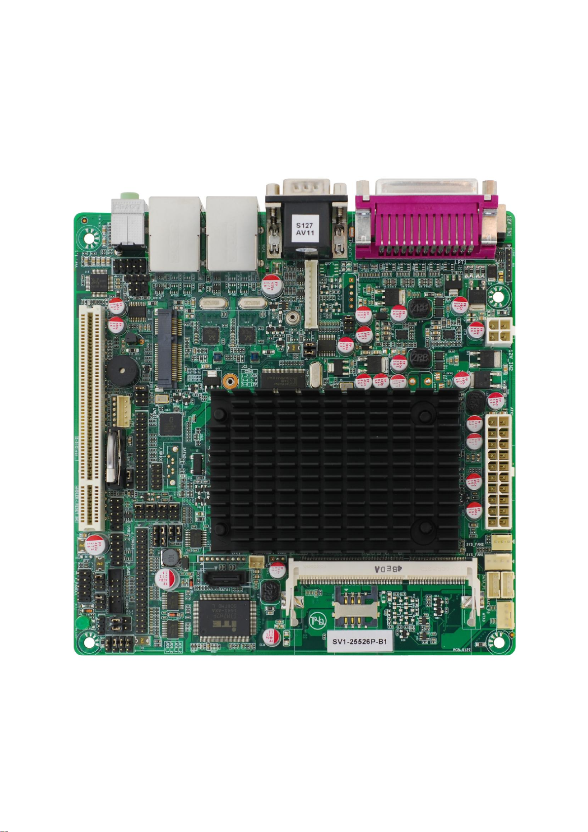
4. Jumpers / Headers and Connectors

- 7 -
- 8 -
Jumpers/Headers/Connectors
1
ATX3 Power Output Connector
P10
24
RJ11 Header [2]
P17
2
Front USB Headers
P10
25
SATA Power Headers
P17
3
USB(Rear IO)Power Control Jumpers
P10 26
SATA DOM Power Supply Header
P18
4
GPIO Header
P10 27
System Fan1 Header
P18
5
COM1 Control Jumper
P11 28
System Fan2 Header
P18
6
COM2 Header
P11 29
ATX Power Input Connector
7
COM2 Control Jumpers
P11 30
DC12V Power Input Connector
8
COM3-6 Header
P12 31
SO-DIMM Slot
9
COM3 Control Jumpers
P13 32
Mini PCI-E1 Slot
10
COM4 Control Jumpers
P13 33
SIM Card Slot
11
COM5 & COM6 Control Jumpers
P14
34
SATA Connectors
12
RS485 Header
P14
35
Mini PCI-E2 Slot
13
RS232 or RS485 Selection Jumpers
P14
36
LPT Connector
14
LVDS Header
P15
37
COM1(DB9) Connector
15
LVDS VCC Selection Jumper
P15
38
LAN Connectors
16
LVDS Backlight Control Header
P15
39
Audio Connector
17
VGAHeader
P16
40
USB Connectors
18
Front Panel Header
P16
41
VGAConnector
19
Front Audio Header
P16
42
DC Power Output Connector [1]
20
CD IN Header
P16
43
HDMI or RJ11 Port (Cash Drawer)
Connector [2]
P19
21
Audio Amplifier Header
P17
44
PS/2 Keyboard Connector
22
CMOS Clear Jumper
P17
45
DC 12V Power Input Connector [3]
23
Keyboard and Mouse Header
P17

- 9 -
Notes:
[1]: The inner diameter of DC power output connector is 2.0 mm .
[2]: The default power input of RJ11 port (Location 43) is +12V, and it also can be +24V by using RJ11
header (Location 24).
[3]: The inner diameter of DC 12V power input connector is 2.5 mm .
- 10 -
5. Definition of Jumpers/Headers and Connectors
[1] ATX3 Power Output Connector(4*1 Pin 2.54mm)
Location
Connector
Pin
Definition
Pin
Definition
ATX3
1
+ 12V
2
GND
3
GND
4
+ 5V
[2] Front USB Headers(5*2 Pin 2.54mm)
Location
Header
Pin
Definition
Pin
Definition
F_USB1
1
+ 5 V
2
+ 5 V
3
USB4-
4
USB5-
5
USB4+
6
USB5+
7
GND
8
GND
10
N/C
F_USB2
1
+ 5 V
2
+ 5 V
3
USB6-
4
USB7-
5
USB6+
6
USB7+
7
GND
8
GND
10
N/C
[3] USB(Rear IO)Power Control Jumpers(2*1 Pin 2.54mm)
Location
Jumper
Setting
Function
JRU1
JRU2
1-2(Default)
USB(Rear IO) Enable
Without Jumper
USB(Rear IO) Disable
[4] GPIO Header(5*2 Pin 2.00mm)
Location
Header
Pin
Definition
Pin
Definition
J_GPIO1
1
GPO26(0x50F Bit2)
2
GPI22(0x50E Bit6)
3
GPI12(0x50D Bit4)
4
GPI38(0x538 Bit6)
5
GND
6
GPO27(0x50F Bit3)
7
GPO33(0x538 Bit1)
8
GPO36(0x538 Bit4)
9
GPI39(0x538 Bit7)
10
+ 5V *
*The value is 3.3V or 5V selectable (need hardware supported), and the default value is 5V.

- 11 -
[5] COM1 Control Jumper(3*2 Pin 2.00mm)
Location
Jumper
Setting
Function
JC1_1
1-2(Default)
Pin1:DCD
3-4
Pin1:+5V
5-6
Pin1:+12V
[6] COM2 Header(5*2 Pin 2.00mm)
Location
Jumper
Pin
Definition
Pin
Definition
J_COM2
1
JC2_1*
2
RXD
3
TXD
4
DTR
5
GND
6
DSR
7
RTS
8
CTS
9
JC2_2*
*These signals are depend on relevant Jumpers (e.g. Pin1 of J_COM2 depends on JC2_1 Jumper),
to find more details, check the following table (Location 7).
[7] COM2 Control Jumpers(3*2 Pin 2.00mm)
Location
Jumper
Setting
Function
JC2_1
1-2(Default)
Pin1:DCD
3-4
Pin1:+5V
5-6
Pin1:+12V
JC2_2
1-2(Default)
Pin9:RI
3-4
Pin9:+5V
5-6
Pin9:+12V

- 12 -
[8] COM3-6 Header(20*2 Pin 2.00mm)
Location
Header
Pin
Definition
Pin
Definition
J_COM3~6
1
JC3_1*
2
JC3_3*,JC3_5*
3
JC3_4*,JC3_6*
4
DTR3
5
GND
6
DSR3
7
RTS3
8
JC3_5*
9
JC3_2,JC3_6*
10
GND
11
JC4_1*
12
RXD4
13
TXD4
14
DTR4
15
GND
16
DSR4
17
RTS4
18
CTS4
19
JC4_2*
20
GND
21
JC5_1*
22
RXD5
23
TXD5
24
DTR5
25
GND
26
DSR5
27
RTS5
28
CTS5
29
JC5_2*
30
GND
31
JC6_1*
32
RXD6
33
TXD6
34
DTR6
35
GND
36
DSR6
37
RTS6
38
CTS6
39
JC6_2*
40
GND
*These signals are depend on relevant Jumpers (e.g. Pin1 of J_COM3 depends on JC3_1 Jumper),
to find more details, check the following tables (Location 9~11).

- 13 -
[9] COM3 Control Jumpers(3*2/4*1 Pin 2.00mm)
Location
Jumper
Setting
Function
JC3_1
1-2(Default)
Pin1:DCD
3-4
Pin1:+5V
5-6
Pin1:+12V
JC3_2
1-2(Default)
Pin9:RI
3-4
Pin9:+5V
5-6
Pin9:+12V
JC3_3
JC3_4
1-2,3-4(Default)
RS-232
2-3
TTL
JC3_5
1-2(Default)
Pin8:CTS
2-3
Pin8:Same value as Pin2
JC3_6
1-2(Default)
N/C
2-3
Pin9:Same value as Pin3
[10] COM 4 Control Jumpers(3*2 Pin 2.00mm)
Location
Jumper
Setting
Function
JC4_1
1-2(Default)
Pin1:DCD
3-4
Pin1:+5V
5-6
Pin1:+12V
JC4_2
1-2(Default)
Pin9:RI
3-4
Pin9:+5V
5-6
Pin9:+12V

- 14 -
[11] COM5 & COM6 Control Jumpers(3*1 Pin 2.00mm)
Location
Jumper
Setting
Function
JC5_1
1-2(Default)
COM5_Pin 1:DCD
2-3
COM5_Pin 1:+5V or +12V
JC5_2
1-2(Default)
COM5_Pin 9:RI
2-3
COM5_Pin 9:+5V or +12V
JC6_1
1-2(Default)
COM6_Pin 1:DCD
2-3
COM6_Pin 1:+5V or +12V
JC6_2
1-2(Default)
COM6_Pin 9:RI
2-3
COM6_Pin 9:+5V or +12V
Notes:
[1]: Pin1 and Pin9 of COM5 and COM6 can be +5V or +12V (need hardware supported), but the voltage
of these 4 Pins must be the same.
[12] RS485 Header(3*1 Pin 2.54mm)
Location
Header
Pin
Definition
Pin
Definition
JC6_5
1
RS485-
2
GND
3
RS485+
[13] RS232 or RS485 Selection Jumpers(3*1 Pin 2.54mm)
Location
Jumper
Settings
Working Mode
JC6_3
JC6_4
1-2(Default)
J_COM6(RS232)
2-3
JC6_5(RS485)
Notes:
[1]: COM6(RS232) Header and JC6_5(RS485) Header can’t be used at the same time, by setting RS232
or RS485 Selection Jumpers(JC6_3, JC6_4 Location 13) can decide which one is available .

- 15 -
[14] LVDS Header(15*2 Pin 2.00mm)
Location
Header
Pin
Definition
Pin
Definition
LVDS1
1
VCC*
2
VCC*
3
VCC*
4
N/C
5
GND
6
GND
7
LVDS_A_DATA0-
8
LVDS_A_DATA0+
9
LVDS_A_DATA1-
10
LVDS_A_DATA1+
11
LVDS_A_DATA2-
12
LVDS_A_DATA2+
13
GND
14
GND
15
LVDS_A_CLK-
16
LVDS_A_CLK+
17
LVDS_A_DATA3-
18
LVDS_A_DATA3+
19
LVDS_B_DATA0-
20
LVDS_B_DATA0+
21
LVDS_B_DATA1-
22
LVDS_B_DATA1+
23
LVDS_B_DATA2-
24
LVDS_B_DATA2+
25
GND
26
GND
27
LVDS_B_CLK-
28
LVDS_B_CLK+
29
LVDS_B_DATA3-
30
LVDS_B_DATA3+
* VCC could be 3.3V(default) or 5V or 12V by setting the LVDS VCC Selection Jumper(LVDS_P2,
Location 15).
[15] LVDS VCC Selection Jumper(3*2 Pin 2.54mm)
Location
Jumper
Setting
Function
LVDS_P2
1-2(Default)
+ 3.3V
3-4
+ 5V
5-6
+ 12V
[16] LVDS Backlight Control Header(5*1 Pin 2.00mm)
Location
Header
Pin
Definition
Pin
Definition
LVDS_P1
1
+ 12V
2
GND
3
LVDS_BKL_EN
4
N/C
5
+ 5V

- 16 -
[17] VGA Connector(12*1 Pin 2.00mm)
Location
Connector
Pin
Definition
Pin
Definition
J_VGA1
1
CRT_ON
2
VSYNC
3
HSYNC
4
GND
5
RED
6
GND
7
GREEN
8
GND
9
BLUE
10
GND
11
DDCDAT
12
DDCCLK
[18] Front Panel Header(5*2 Pin 2.54mm)
Location
Header
Pin
Definition
Pin
Definition
F_PANEL1
1
HD LED+
2
Power LED+
3
HD LED-
4
Power LED-
5
RESET-
6
PWR+
7
RESET+
8
PWR -
9
N/C
[19] Front Audio Header(5*2 Pin 2.54mm)
Location
Header
Pin
Definition
Pin
Definition
F_AUDIO1
1
FP_MIC_L
2
GND
3
FP_MIC_R
4
+ 3.3 V
5
FP_OUT_R
6
Jack Detect
7
GND
9
FP_OUT_L
10
Jack Detect
[20] CD IN Header(4*1 Pin 2.54mm)
Location
Header
Pin
Definition
Pin
Definition
CD1
1
CD_IN_L
2
CD_GND
3
CD_GND
4
CD_IN_R

- 17 -
[21] Audio Amplifier Header(3*2 Pin 2.54mm)
Location
Header
Pin
Definition
Pin
Definition
F_AUDIO2
1
SPKR_R-
2
SPKR_L-
3
SPKR_R+
4
SPKR_L+
6
GND
[22] CMOS Clear Jumper(3*1 Pin 2.54mm)
Location
Jumper
Setting
Function
JCMOS1
1-2(Default)
Normal
2-3
Clear CMOS
[23] Keyboard and Mouse Header(6*1 Pin 2.00mm)
Location
Header
Pin
Definition
Pin
Definition
J_KBMS1
1
KB_CLK
2
KB_DATA
3
MS_CLK
4
GND
5
+ 5V
6
MS_DATA
[24] RJ11 Header(5*1 Pin 2.00mm)
Location
Header
Pin
Definition
Pin
Definition
JRJ11_1
1
+ 24V
2
N/C
3
N/C
4
GND
5
GND
[25] SATA Power Supply Headers(4*1 Pin 2.00mm)
Location
Header
Pin
Definition
Pin
Definition
SATA_P1
1
+ 12V
2
GND
3
GND
4
+ 5V
SATA_P2
1
+ 12V
2
GND
3
GND
4
+ 5V

- 18 -
[26] SATA DOM Power Supply Header(2*1 Pin 2.00mm)
Location
Header
Pin
Definition
Pin
Definition
JSAP1
1
GND
2
+ 5V
[27] System Fan1 Header(4*1 Pin 2.54mm)
Location
Header
Pin
Definition
Pin
Definition
SYS_FAN1
1
GND
2
+ 12V
3
FAN Speed Detection
4
FAN Speed Control
[28] System Fan2 Header(3*1 Pin 2.54mm)
Location
Header
Pin
Definition
Pin
Definition
SYS_FAN2
1
GND
2
+ 12V
3
N/C
[29] SIM Card Header(6*1 Pin 2.00mm)OPTIONAL
Header
Pin
Definition
Pin
Definition
J_SIM1
1
UIM_PWR
2
UIM_RESET
3
UIM_CLK
4
GND
5
UIM_VPP
6
UIM_DAT
[30] SATA1 Pin7 Control Jumper(3*1 Pin 2.00mm)OPTIONAL
Jumper
Settings
Function
JSD1
1-2(Default)
PIN7:GND
2-3
PIN7:+5V

- 19 -
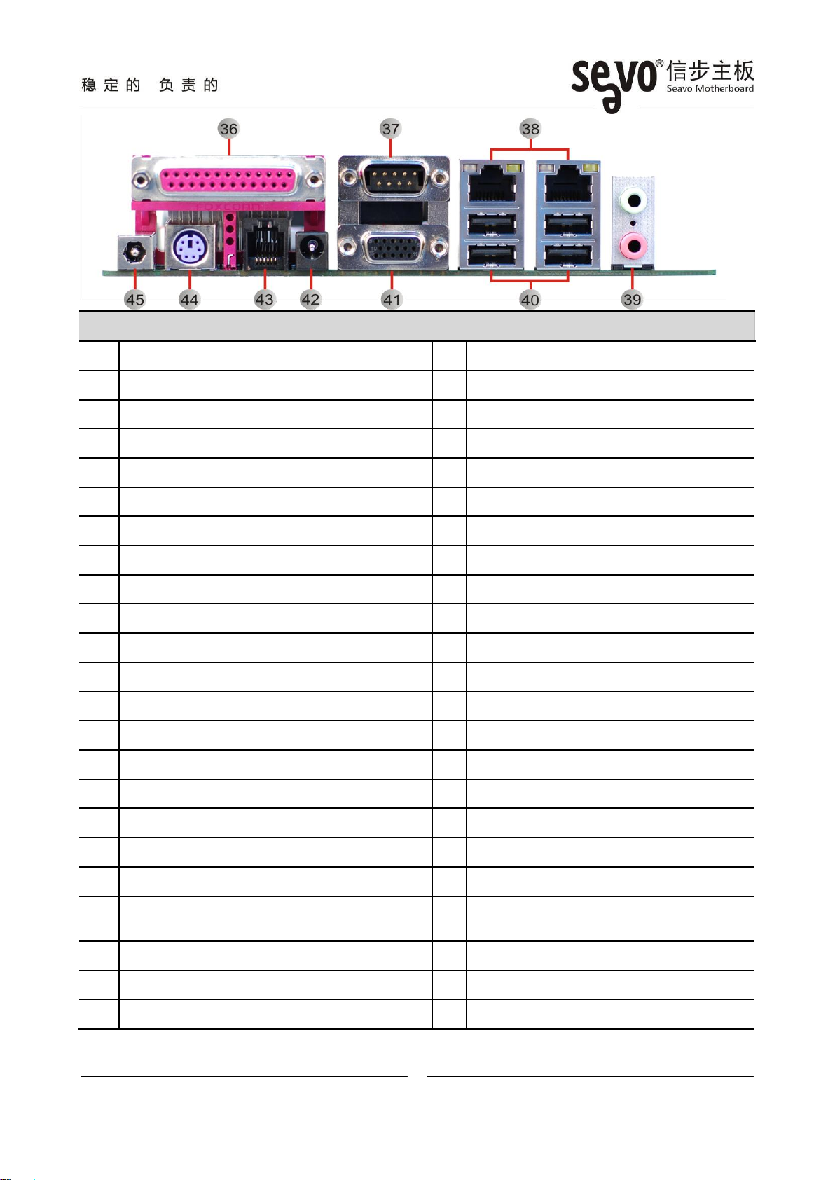
6. Definitions of some rear I/O Connectors
[43] RJ11 Port (Cash Drawer) Connector (6 Pin)
Location
Graphic
Pin
Definition
Pin
Definition
1
GND
2
Cash Drawer Control
(SB_GPO8: 50D Bit0)
3
Cash Drawer Detect
(SB_GPI10: 50D Bit2)
4
Cash Drawer Power *
5
N/C
6
GND
*To find the value of Cash Drawer Power, check the Note [2] in Page 8.
【End】
Table of contents
Other Seavo Motherboard manuals


