Seavo SV3b-64126 Series User manual

SV3b-64126 Series
Ver 1.0
User's Manual
Seavo Motherboard
用户手册
- 1 -
深圳市信步科技有限公司 地址:深圳市福田区车公庙泰然科技园 210 栋西座 5H T 86-755-88251900 F 86-755-88251910 www.seavo.com
Contents
1. Models and Attentions ................................................................................................... 2
1.1 Models ............................................................................................................................................ 2
1.2 Attentions ........................................................................................................................................ 2
2. Specification .................................................................................................................. 3
3. Functional Block Diagram ..............................................................................................5
4. Mechanical Drawing ...................................................................................................... 6
5. Jumpers / Headers and Connectors ..............................................................................7
6. Definition of Jumpers /Headers and Connectors ......................................................... 10
1) PWR_LED1 (Power LED Header 2*1 Pin 1.25mm) ...................................................................10
2) PANSW1 (Power Button Header 2*1 Pin 1.25mm) ....................................................................10
3) SYSRST1 (System Reset Header 2*1 Pin 1.25mm) ..................................................................10
4) HDD_LED1 (HDD LED Header 2*1 Pin 1.25mm) ......................................................................10
5) CPU_FAN1 (CPU FAN Header 4*1 Pin 1.25mm) ...................................................................... 10
6) JC_LVDS1 (LVDS VDD Select Jumper 3*2 Pin 2.54 mm) ......................................................... 11
7) LVDS1 (LVDS Signal Header 20*2 Pin 1.25mm) ....................................................................... 11
8) LVDS_P1 (LVDS Backlight Control Header 6*1 Pin 2.00mm) ................................................... 12
9) J_COM4/5/6/6_1 (COM4/5/6/6_1 Header 3*1 Pin 2.00mm) ..................................................... 12
10) J_SIM1 (SIM Card Header 6*1 Pin 1.25mm) ............................................................................. 12
11) J_COM1/2/3 (COM1/2/3 Header 9*1 Pin 1.25mm) ....................................................................13
12) BAT1 (CMOS Battery Header 2*1 Pin 1.25mm) .........................................................................13
13) J_GPIO1 (GPIO Header 5*2 Pin 2.00mm) ................................................................................. 14
14) P_SATA1 (SATA Power Header 4*1 Pin 2.00mm) ..................................................................... 14
15) F_USB1 (Front USB2.0 Header1 5*2 Pin 2.00mm) ...................................................................14
16) F_USB2 (Front USB2.0 Header2 4*1 Pin 2.00mm) ...................................................................14
17) F_USB3 (Front USB2.0 Header3 4*1 Pin 2.00mm) ...................................................................15
18) J_SPK1 (Amplifier Header 2*1 Pin 1.25mm) ..............................................................................15
19) CLR_CMOS1 (CMOS Clear Jumper 3*1 Pin 2.00mm) ..............................................................15
20) J_MPS1 (MPS Header 4*1 Pin 1.25mm) ................................................................................... 15
26) J_GSPI1 (GSPI Header1 8*1 Pin 1.25mm) ................................................................................15
27) J_GSPI2 (GSPI Header2 8*1 Pin 1.25mm) ................................................................................16
34) LAN2 (GBE LAN RJ45 Connector2 8Pin) .................................................................................. 16
35) LAN1 (GBE LAN RJ45 Connector1 8Pin) .................................................................................. 16
7. BIOS setup .................................................................................................................. 17
- 2 -
深圳市信步科技有限公司 地址:深圳市福田区车公庙泰然科技园 210 栋西座 5H T 86-755-88251900 F 86-755-88251910 www.seavo.com
1.Models and Attentions
1.1 Models
This manual is applied to following models:
1.2 Attentions
1) Notes under a table or figure indicate the difference of models, or alternative definition of
specific pin of the header (jumper/connector).
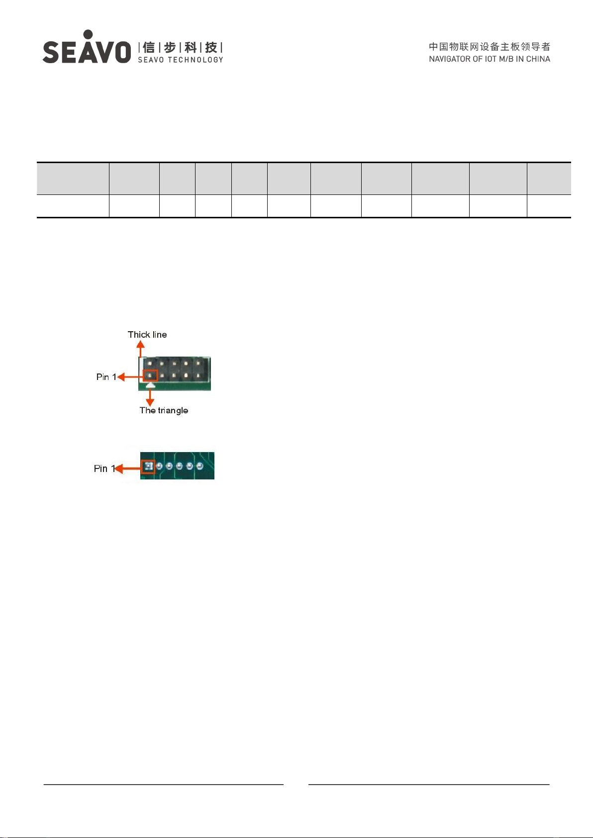
2) How to identify the first pin of a header or jumper
Usually, there is a thick line or a triangle near the header’s or jumper’s pin 1.
Square pad, which you can find on the back of the motherboard, is usually used for pin 1.
Model
CPU
COM
LAN
USB
HDMI
eDP/
LVDS
MINI-
PCIE
M.2
Key-B
M.2
Key-M
SATA
3.0
SV3b-64126
J6412
6
2
10
2
LVDS
mSATA
USB3.0
PCIe x2
1
- 3 -
深圳市信步科技有限公司 地址:深圳市福田区车公庙泰然科技园 210 栋西座 5H T 86-755-88251900 F 86-755-88251910 www.seavo.com
2.Specification
Model
SV3b-64126
CPU
Intel® Celeron® J6412, Quad-core, clock speed 2.00 GHz, up to 2.60GHz, TDP 10W
Display
1 * eDP1/LVDS (Header): LVDS max resolution up to 1920x1200 @ 60Hz (default)
or eDP max resolution up to 3840x2160 @ 60Hz 30bpp or
4096x2304 @ 60Hz 24bpp
2 * HDMI (TYPE-A): max resolution up to 4096x2160 @ 30 Hz
Memory
Support DDR4-2666/2933/3200MHz, 1 * non-ECC SO-DIMM Slot, Up to 32GB
Storage
1 * SATA3.0 7P Connector (With 1 * SATA Power Header) [1]
1 * Mini PCI-E Slot (USB2.0+PCIE/mSATA, default mSATA) [2]
Ethernet
2 * Intel I225-V GBE LAN Chip (RJ45, 10/100/1000 Mbps)
Audio
Realtek Audio HDA Codec
1 * Line-Out + MIC 2in1 3.5mm Jack
1 * Amplifier Header, 3W into an 4ΩLoads
Expansion Slots
1 * M.2 Key-M Slot (PCIe x2 NVMe SSD, 2280) [1][3]
1 * M.2 Key-B Slot (PCIE/USB3.0+ USB2.0,3052, default USB3.0, Support 5G) [2][4]
COM
3 * RS232 (COM1/2/3, Header, Full Wires)
2 * RS232/TTL (COM4/5, Header, 2 Wires)
1 * RS232/RS485/TTL (COM6, Header, 2 Wires)
USB
3 * USB3.0 (TYPE-A, Rear IO)
3 * USB2.0 (TYPE-A, Rear IO)
4 * USB2.0 (Header, Internal)
Other Ports
8 * GPIO Header
1 * Power LED Header
1 * Power Button Header
1 * System Reset Header
1 * HDD LED Header
1 * CPU FAN Header
1 * MPS Header
2 * GSPI Header
1 * SIM Card Header
System
Windows 10 64-bit, Linux
Temperature
Storage: -20~75℃
Operating: 0~60℃
BIOS
AMI UEFI BIOS (Support Watchdog Timer)
Power Supply
DC 12V
1 * DC 12V Power Input Φ2.5mm Jack (ATX 4P/ Wafer optional)
Factor
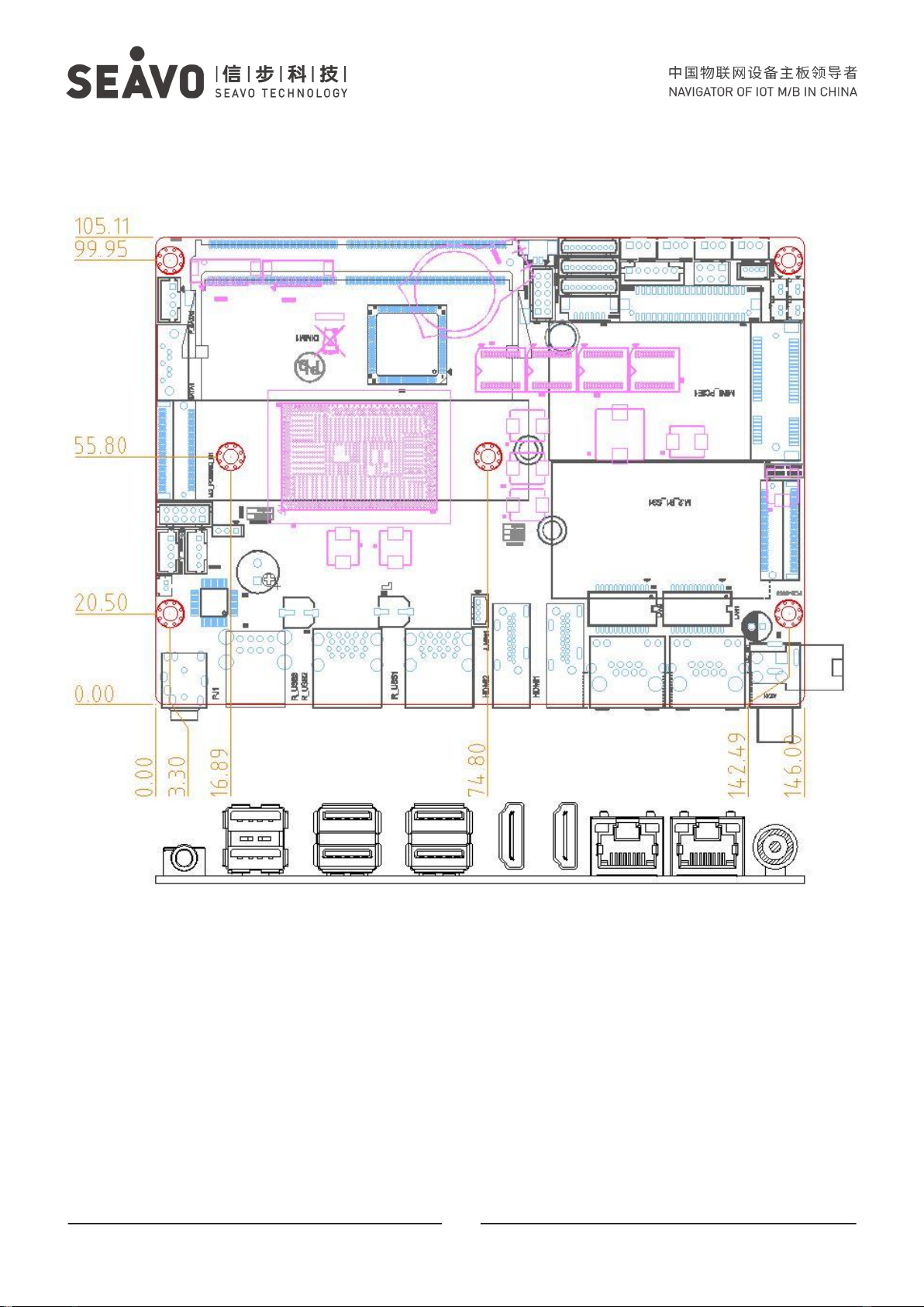
146mm*105mm

- 4 -
深圳市信步科技有限公司 地址:深圳市福田区车公庙泰然科技园 210 栋西座 5H T 86-755-88251900 F 86-755-88251910 www.seavo.com
Notes:
[1]: M.2 key-M slot supports PCIe x2 NVMe /SATA SSD, sel by res. Colay SATA signal with SATA3.0 7P connector.
[2]: Mini PCI-E Slot supports SATA/PCIE+USB2.0, sel by res. Colay SATA signal with M.2 key-B slot. Colay USB2.0 signal with
F_USB3 Header.
[3]: PCIe x2 Gen3/Gen4 determined by the CPU.
[4]: M.2 key-B slot supports PCIE/USB3.0/mSATA+ USB2.0, sel by res. Colay SATA signal with Mini PCI-E slot. Colay USB2.0
signal with F_USB2 Header. Colay PCIE/USB3.0 signal with R_USB2_UP Connector.
- 5 -
深圳市信步科技有限公司 地址:深圳市福田区车公庙泰然科技园 210 栋西座 5H T 86-755-88251900 F 86-755-88251910 www.seavo.com
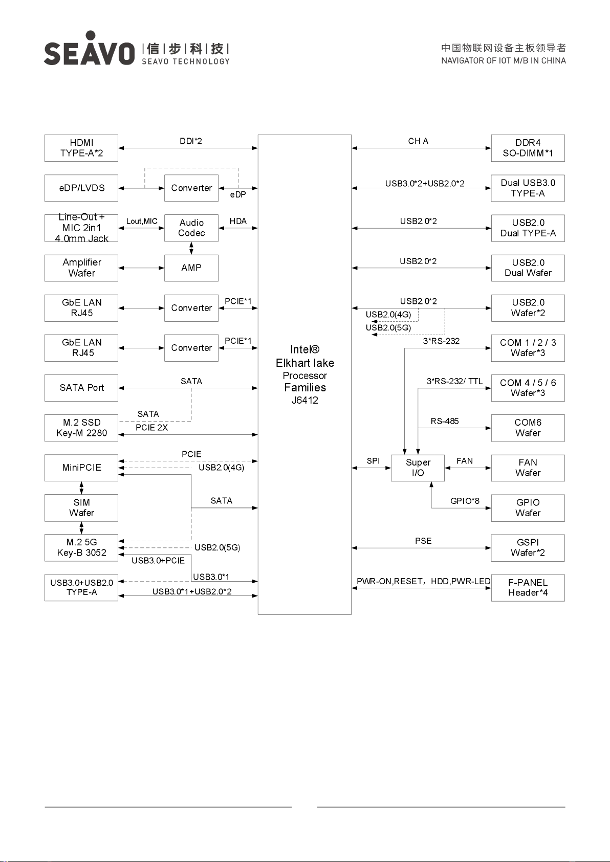
3.Functional Block Diagram
- 6 -
深圳市信步科技有限公司 地址:深圳市福田区车公庙泰然科技园 210 栋西座 5H T 86-755-88251900 F 86-755-88251910 www.seavo.com
4.Mechanical Drawing
- 7 -
深圳市信步科技有限公司 地址:深圳市福田区车公庙泰然科技园 210 栋西座 5H T 86-755-88251900 F 86-755-88251910 www.seavo.com
5. Jumpers / Headers and Connectors
- 8 -
深圳市信步科技有限公司 地址:深圳市福田区车公庙泰然科技园 210 栋西座 5H T 86-755-88251900 F 86-755-88251910 www.seavo.com
Jumpers / Headers and Connectors
PWR_LED1
Power LED Header
PANSW1
Power Button Header
SYSRST1
System Reset Header
HDD_LED1
HDD LED Header
CPU_FAN1
CPU FAN Header
JC_LVDS1
LVDS VDD Select Jumper
LVDS1
LVDS Signal Header
LVDS_P1
LVDS Backlight Control Header
J_COM4/5/6/6_1
COM4/5/6/6_1 Header
J_SIM1
SIM Card Header
J_COM1/2/3
COM1/2/3 Header
BAT1
CMOS Battery Header
J_GPIO1
GPIO Header
P_SATA1
SATA Power Header
F_USB1
Front USB2.0 Header1
F_USB2
Front USB2.0 Header2

- 9 -
深圳市信步科技有限公司 地址:深圳市福田区车公庙泰然科技园 210 栋西座 5H T 86-755-88251900 F 86-755-88251910 www.seavo.com
F_USB3
Front USB2.0 Header3
J_SPK1
Amplifier Header
CLR_CMOS1
CMOS Clear Jumper
J_MPS1
MPS Header
M.2_B1_5G1
M.2 (NGFF) Key-B Slot (PCIE/USB3.0+USB2.0, 3052/3042,
Support 4G/5G)
MINI_PCIE1
Mini PCI-E Slot (mSATA)
DIMM1
DDR4 SO-DIMM Slot
SATA1
SATA3.0 7P Connector
M.2_PCIESSD_M1
M.2 (NGFF) Key-M Slot (PCIe x2 NVMe SSD, 2280)
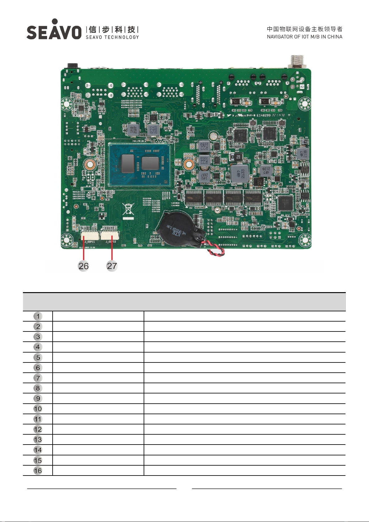
J_GSPI1
GSPI Header1
J_GSPI2
GSPI Header2
PJ1
Line-Out + MIC 2in1 4.0mm Jack
R_USB3
Dual USB2.0 TYPE-A Connector
R_USB2
Dual USB3.0 TYPE-A Connector
R_USB1
Dual USB3.0 TYPE-A Connector
HDMI2
HDMI Upright TYPE-A Connector2
HDMI1
HDMI Upright TYPE-A Connector1
LAN2
GBE LAN RJ45 Connector2
LAN1
GBE LAN RJ45 Connector1
DC_IN1(ATX1/DC_IN2)
DC 12V Power Input Φ2.5mm Jack (ATX 4P/ Wafer optional)

- 10 -
深圳市信步科技有限公司 地址:深圳市福田区车公庙泰然科技园 210 栋西座 5H T 86-755-88251900 F 86-755-88251910 www.seavo.com
6.Definition of Jumpers /Headers and Connectors
1) PWR_LED1 (Power LED Header 2*1 Pin 1.25mm)
Graphic
Pin
Definition
Pin
Definition
1
+ 3.3V
2
GND
2) PANSW1 (Power Button Header 2*1 Pin 1.25mm)
Graphic
Pin
Definition
Pin
Definition
1
PANSWH#
2
GND
3) SYSRST1 (System Reset Header 2*1 Pin 1.25mm)
Graphic
Pin
Definition
Pin
Definition
1
SYS_RESET#
2
GND
4) HDD_LED1 (HDD LED Header 2*1 Pin 1.25mm)
Graphic
Pin
Definition
Pin
Definition
1
+ 3.3V
2
HD_LED#
5) CPU_FAN1 (CPU FAN Header 4*1 Pin 1.25mm)
Graphic
Pin
Definition
Pin
Definition
1
GND
3
FAN Speed Detection
2
+ 5V [1]
4
FAN Speed Control
Notes:
[1]: Power of CPU_FAN1 is + 5V by default, can support + 12V if specified. (resistor selectable)

- 11 -
深圳市信步科技有限公司 地址:深圳市福田区车公庙泰然科技园 210 栋西座 5H T 86-755-88251900 F 86-755-88251910 www.seavo.com
6) JC_LVDS1 (LVDS VDD Select Jumper 3*2 Pin 2.54 mm)
Graphic
Setting
Function
1-2(Default)
3.3V
3-4
5V
5-6
12V
7) LVDS1 (LVDS Signal Header 20*2 Pin 1.25mm)
Graphic
Pin
Definition
Pin
Definition
2
VDD_PANEL [1]
1
VDD_PANEL [1]
4
GND
3
LVDS_PRSNT#
6
VDD_PANEL [1]
5
VDD_PANEL [1]
8
LVDS_B_DATA0-/
EDP1_TX0- [2]
7
LVDS_A_DATA0-
10
LVDS_B_DATA0+/
EDP1_TX0+ [2]
9
LVDS_A_DATA0+
12
GND
11
GND
14
LVDS_B_DATA1-/
EDP1_TX1- [2]
13
LVDS_A_DATA1-
16
LVDS_B_DATA1+/
EDP1_TX1+ [2]
15
LVDS_A_DATA1+
18
GND
17
GND
20
LVDS_B_DATA2-/
EDP1_TX2- [2]
19
LVDS_A_DATA2-
22
LVDS_B_DATA2+/
EDP1_TX2- [2]
21
LVDS_A_DATA2+
24
GND
23
GND
26
LVDS_B_CLK-/
EDP1_TX3- [2]
25
LVDS_A_CLK-
28
LVDS_B_CLK+/
EDP1_TX1+ [2]
27
LVDS_A_CLK+
30
GND
29
GND
32
EDP1_HPD_C
31
N/C
34
GND
33
GND
36
LVDS_B_DATA3-/
EDP1_AUX- [2]
35
LVDS_A_DATA3-
38
LVDS_B_DATA3+/
EDP1_AUX+ [2]
37
LVDS_A_DATA3+

- 12 -
深圳市信步科技有限公司 地址:深圳市福田区车公庙泰然科技园 210 栋西座 5H T 86-755-88251900 F 86-755-88251910 www.seavo.com
40
GND
39
N/C
Notes:
[1]: Panel Power VDD can be 3.3V (default) /5V/12V selectable by “LVDS1 VDD Select Jumper”.
(JC_LVDS1, Location 6).
[2]: It supports LVDS by default, and it also can support eDP if specified. (BOM selectable).
8) LVDS_P1 (LVDS Backlight Control Header 6*1 Pin 2.00mm)
Graphic
Pin
Definition
Pin
Definition
1
GND
4
LVDS _BKLT_EN
2
GND
5
+ 12V
3
LVDS_BKLT_CTL
6
+ 12V
9) J_COM4/5/6/6_1 (COM4/5/6/6_1 Header 3*1 Pin 2.00mm)
Graphic
Pin
Definition
Pin
Definition
J_COM4
1
COM4_RXD
3
GND
2
COM4_TXD
Graphic
Pin
Definition
Pin
Definition
J_COM5
1
COM5_RXD
3
GND
2
COM5_TXD
Graphic
Pin
Definition
Pin
Definition
J_COM6
1
COM6_RXD
3
GND
2
COM6_TXD
Graphic
Pin
Definition
Pin
Definition
J_COM6_1
1
COM6_RS485+
3
GND
2
COM6_RS485-
10) J_SIM1 (SIM Card Header 6*1 Pin 1.25mm)
Graphic
Pin
Definition
Pin
Definition
1
UIM1_PWR
4
UIM1_CLK
2
UIM1_DAT
5
UIM1_RST
3
GND
6
UIM1_VPP

- 13 -
深圳市信步科技有限公司 地址:深圳市福田区车公庙泰然科技园 210 栋西座 5H T 86-755-88251900 F 86-755-88251910 www.seavo.com
11) J_COM1/2/3 (COM1/2/3 Header 9*1 Pin 1.25mm)
Graphic
Pin
Definition
Pin
Definition
J_COM1
1
COM1_ PIN1 [1]
6
COM1_CTS#
2
COM1_DSR#
7
COM1_DTR#
3
COM1_RXD
8
COM1_PIN9 [2]
4
COM1_RTS#
9
GND
5
COM1_TXD
Notes:
[1]: PIN1 of J_COM1 is DCD# by default, 5V/12V is selectable. (resistor selectable)
[2]: PIN9 of J_COM1 is RI# by default, 5V is selectable. (resistor selectable)
Graphic
Pin
Definition
Pin
Definition
J_COM2
1
COM2_ PIN [1]
6
COM2_CTS#
2
COM2_DSR#
7
COM2_DTR#
3
COM2_RXD
8
COM2_PIN9 [2]
4
COM2_RTS#
9
GND
5
COM2_TXD
Notes:
[1]: PIN1 of J_COM2 is DCD# by default, 5V/12V is selectable. (resistor selectable)
[2]: PIN9 of J_COM2 is RI# by default, 5V is selectable. (resistor selectable)
Graphic
Pin
Definition
Pin
Definition
J_COM3
1
COM3_ PIN1 [1]
6
COM3_CTS#
2
COM3_DSR#
7
COM3_DTR#
3
COM3_RXD
8
COM3_PIN9 [2]
4
COM3_RTS#
9
GND
5
COM3_TXD
Notes:
[1]: PIN1 of J_COM3 is DCD# by default, 5V/12V is selectable. (resistor selectable)
[2]: PIN9 of J_COM3 is RI# by default, 5V is selectable. (resistor selectable)
12) BAT1 (CMOS Battery Header 2*1 Pin 1.25mm)
Graphic
Pin
Definition
Pin
Definition
1
+ 3.3V
2
GND

- 14 -
深圳市信步科技有限公司 地址:深圳市福田区车公庙泰然科技园 210 栋西座 5H T 86-755-88251900 F 86-755-88251910 www.seavo.com
13) J_GPIO1 (GPIO Header 5*2 Pin 2.00mm)
Graphic
Pin
Definition
Pin
Definition
2
SIO_GPI70
(0xA06 Bit0, H [1])
1
SIO_GPI71
(0xA06 Bit1, H [1])
4
SIO_GPI72
(0xA06 Bit2, H [1])
3
SIO_GPI73
(0xA06 Bit3, H [1])
6
SIO_GPO74
(0xA06 Bit4, H [1])
5
SIO_GPO75
(0xA06 Bit5, H [1])
8
SIO_GPO76
(0xA06 Bit6, H [1])
7
SIO_GPO77
(0xA06 Bit7, H [1])
10
+ 3.3V [2]
9
GND
Notes:
[1]: H” or “L” means the default voltage is High or Low level.
[2]: Power on this Pin is 3.3V by default, 5V is available if specified. (resistor selectable)
14) P_SATA1 (SATA Power Header 4*1 Pin 2.00mm)
Graphic
Pin
Definition
Pin
Definition
1
+ 12V
3
GND
2
GND
4
+ 5V
15) F_USB1 (Front USB2.0 Header1 5*2 Pin 2.00mm)
Graphic
Pin
Definition
Pin
Definition
2
+ 5V
1
+ 5V
4
USB2_9-
3
USB2_10-
6
USB2_9+
5
USB2_10+
8
GND
7
GND
10
N/C
9
GND
16) F_USB2 (Front USB2.0 Header2 4*1 Pin 2.00mm)
Graphic
Pin
Definition
Pin
Definition
1
+ 5V
3
USB2_CN_1+
2
USB2_CN_1-
4
GND

- 15 -
深圳市信步科技有限公司 地址:深圳市福田区车公庙泰然科技园 210 栋西座 5H T 86-755-88251900 F 86-755-88251910 www.seavo.com
17) F_USB3 (Front USB2.0 Header3 4*1 Pin 2.00mm)
Graphic
Pin
Definition
Pin
Definition
1
+ 5V
3
USB2_CN_2+
2
USB2_CN_2-
4
GND
18) J_SPK1 (Amplifier Header 2*1 Pin 1.25mm)
Graphic
Pin
Definition
Pin
Definition
1
SPK_OUT+
2
SPK_OUT-
19) CLR_CMOS1 (CMOS Clear Jumper 3*1 Pin 2.00mm)
Graphic
Setting
Function
1-2(Default)
Normal
2-3
Clear CMOS
20) J_MPS1 (MPS Header 4*1 Pin 1.25mm)
Graphic
Pin
Definition
Pin
Definition
1
VCCIN_SDA
3
VCCIN_PE
2
VCCIN_SCL
4
GND
26) J_GSPI1 (GSPI Header1 8*1 Pin 1.00mm)
Graphic
Pin
Definition
Pin
Definition
1
PSE_SPI0_INT
5
PSE_SPI0_CS0
2
PSE_SPI0_CLK
6
PSE_SPI0_CS1
3
PSE_SPI0_MOSI
7
GND
4
PSE_SPI0_MISO
8
+ 3.3V
- 16 -
深圳市信步科技有限公司 地址:深圳市福田区车公庙泰然科技园 210 栋西座 5H T 86-755-88251900 F 86-755-88251910 www.seavo.com
27) J_GSPI2 (GSPI Header2 8*1 Pin 1.00mm)
Graphic
Pin
Definition
Pin
Definition
1
PSE_SPI3_INT
5
PSE_SPI3_CS0
2
PSE_SPI3_CLK
6
PSE_SPI3_CS1
3
PSE_SPI3_MOSI
7
GND
4
PSE_SPI3_MISO
8
+ 3.3V
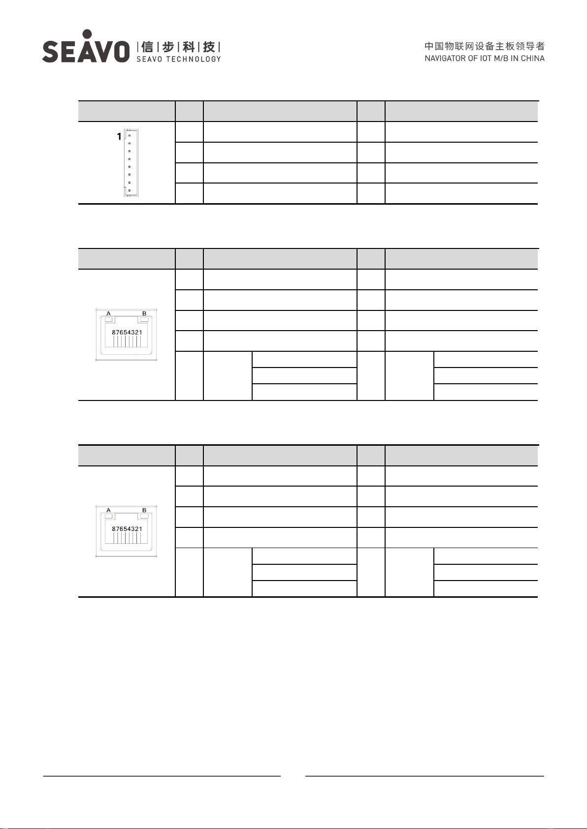
34) LAN2 (GBE LAN RJ45 Connector2 8Pin)
Graphic
Pin
Definition
Pin
Definition
1
XMDI2_0+
5
XMDI2_2-
2
XMDI2_0-
6
XMDI2_1-
3
XMDI2_1+
7
XMDI2_3+
4
XMDI2_2+
8
XMDI2_3+
A
Active
LED
ACT: Twinkling Yellow
B
Speed
LED
1000M: Turn Yellow
Only LINK: Lights Off
100M: Turn Green
Stop: Lights Off
10M: Lights Off
35) LAN1 (GBE LAN RJ45 Connector1 8Pin)
Graphic
Pin
Definition
Pin
Definition
1
XMDI1_0+
5
XMDI1_2-
2
XMDI1_0-
6
XMDI1_1-
3
XMDI1_1+
7
XMDI1_3+
4
XMDI1_2+
8
XMDI1_3+
A
Active
LED
ACT: Twinkling Yellow
B
Speed
LED
1000M: Turn Yellow
Only LINK: Lights Off
100M: Turn Green
Stop: Lights Off
10M: Lights Off

- 17 -
深圳市信步科技有限公司 地址:深圳市福田区车公庙泰然科技园 210 栋西座 5H T 86-755-88251900 F 86-755-88251910 www.seavo.com
7.BIOS setup
See “BIOS Spec for SV3b-64126 Series” for detail information of BIOS setup.
【End】
Table of contents
Other Seavo Motherboard manuals


