Seiko Epson S-MOS SPC8104 User manual

412-1.0
Copyright © 1997 S-MOS Systems Inc. All rights reserved. VDC
This document, and any text derived, extracted or transmitted from it, is the sole property of S-MOS Systems Inc. and may not be used, copied,
transmitted or otherwise made available to any other person, unless specifically allowed under license agreement with S-MOS Systems Inc. If fur-
nished under a license, this document may be used and copied only in accordance with the terms of such license, and with the inclusion of this
copyright notice.No title or ownership of the technology herein is transferred.
The information in this document is subject to change without notice and should not be construed as a commitment by S-MOS Systems Inc.This
document does not necessarily describe any current planned or future product by S-MOS Systems Inc., nor does it represent any commitment to
implement any such product.
1
S-MOS Systems, Inc. • Tel: (408) 922-0200 • Fax: (408) 922-0238 • http://www.smos.com
SPC8104 VGA LCD CONTROLLER
SPC8104Technical Manual
Issue Date: 04/01/97

THIS PAGE INTENTIONALLY BLANK
412-1.0
2S-MOS Systems, Inc. • Tel: (408) 922-0200 • Fax: (408) 922-0238 • http://www.smos.com

412-1.0
SPC8104 SPC8104 Technical Manual
3
S-MOS Systems, Inc. • Tel: (408) 922-0200 • Fax: (408) 922-0238 • http://www.smos.com
1.0 CUSTOMER TECHNICAL SUPPORT
S-MOS Systems provides Technical Support Services to their customers for all its graphics prod-
ucts.Follow the technical support guidelines as listed below for the S-MOS graphics product fam-
ilies — VGA LCD Controllers, LCD Controllers, LCD Driver/Controllers, and LCD Drivers.
On-Line
This Technical Manual and new products can be accessed at
www.smos.com
website
Technical Manuals
S-MOS provides detailed Technical Manuals on all its graphics products. Customers should con-
tact their local sales representative or the nearest S-MOS sales office for a unit.
Evaluation Boards
Customers may borrow evaluation boards for the SPC81xx VGA LCD Controller family and the
SED13xx LCD Controller family by contacting their local sales representative or the nearest S-
MOS sales office.
Technical Support
There are a number of ways to contact GraphicsTechnical Support personnel at S-MOS.For cus-
tomers in the Northeast and North Central United States, please contact the Wakefield S-MOS
office for technical support on all products. For customers in the Southeast and South Central
United States, please contact the Raleigh S-MOS office for technical support on all products. For
all other regions contact S-MOS San Jose.
Sales Inquiries
For pricing, delivery, or any other non-technical inquiry, contact your local sales represen-
tative or the nearest S-MOS sales office.
:
Northern California
S-MOS Systems, Inc.
150 River Oaks Parkway
San Jose, CA 95134
Tel: (408) 922-0200
Fax: (408) 922-0238
North Central
S-MOS Systems Inc., North Central
1450 East American Lane, Suite 1550
Schaumburg, IL 60713
Tel: (847) 517-7667
Fax: (847) 517-7601
Northeast
S-MOS Northeast Systems, Inc.
301 Edgewater Place #120
Wakefield, MA 01880
Tel: (617) 246-3600
Fax: (617) 246-5443
Southeast
S-MOS Southeast Systems, Inc.
4300 Six Forks Road #430
Raleigh, NC 27609
Tel: (919) 781-7667
Fax: (919) 781-6778

THIS PAGE INTENTIONALLY BLANK
412-1.0
4S-MOS Systems, Inc. • Tel: (408) 922-0200 • Fax: (408) 922-0238 • http://www.smos.com

412-1.0
SPC8104 SPC8104 Technical Manual
5
S-MOS Systems, Inc. • Tel: (408) 922-0200 • Fax: (408) 922-0238 • http://www.smos.com
TABLE OF CONTENTS
INTRODUCTION
SPC8104F0A Data Sheet
SPECIFICATION
SPC8104F0A Functional Specification
PROGRAMMER’S REFERENCE
SPC8104F0A BIOS Summary
SPC8104F0A BIOS Functional Specification
SPC8104F0A Programming Notes and Examples
UTILITIES
Software Utility Disk Installation Guidelines
SPC8104F0A SETFONT Display Utility
SPC8104F0A BOLD Display Utility
SPC8104F0A REVERSE Display Utility
SPC8104F0A PWRSAVE Power Save Utility
SPC8104F0A READCHIP Diagnostic Utility
SPC8104F0A WGS Windows Gray-Scale Utility
SPC8104F0A SESHELL Shell Utility
SPC8104F0A SHOWMODE Demonstration Program
SPC8104F0A LCDF Display Utility
SPC8104F0A VRTEXP.EXE Display Utility
SPC8104F0A 8104CFG BIOS Configuration Utility
DRIVERS
SPC8104F0A Windows 3.1 16-Color Panning Display Driver
EVALUATION
SDU8104B0C Rev 1.0 Evaluation Board User's Manual
SPC8104F0A Power Consumption
APPLICATION NOTES
Power Save Mode - Doze Mode 1 Implementation Notes

THIS PAGE INTENTIONALLY BLANK
412-1.0
6S-MOS Systems, Inc. • Tel: (408) 922-0200 • Fax: (408) 922-0238 • http://www.smos.com

412-1.0
Copyright © 1997 S-MOS Systems Inc. All rights reserved. VDC
This document, and any text derived, extracted or transmitted from it, is the sole property of S-MOS Systems Inc. and may not be used, copied,
transmitted or otherwise made available to any other person, unless specifically allowed under license agreement with S-MOS Systems Inc. If fur-
nished under a license, this document may be used and copied only in accordance with the terms of such license, and with the inclusion of this
copyright notice.No title or ownership of the technology herein is transferred.
The information in this document is subject to change without notice and should not be construed as a commitment by S-MOS Systems Inc.This
document does not necessarily describe any current planned or future product by S-MOS Systems Inc., nor does it represent any commitment to
implement any such product.
DS-1
S-MOS Systems, Inc. • Tel: (408) 922-0200 • Fax: (408) 922-0238 • http://www.smos.com
SPC8104 VGA LCD CONTROLLER
Data Sheet

THIS PAGE INTENTIONALLY BLANK
412-1.0
DS-2 S-MOS Systems, Inc. • Tel: (408) 922-0200 • Fax: (408) 922-0238 • http://www.smos.com
412-1.0
SPC8104 Data Sheet
DS-3
S-MOS Systems, Inc. • Tel: (408) 922-0200 • Fax: (408) 922-0238 • http://www.smos.com
■
DESCRIPTION
The SPC8104 is a low power, mixed 2.5/3.3 volt graphics controller based on VGA architecture
and optimized for driving a 640x480 LCD panel display.VGA standard mode functionality (with
the exception of mode 13h) is supported using standard IBM VGA parameters. A proprietary
64x4-bit gray scale lookup table is provided to allow re-mapping of the 16 possible gray shades
displayed on an LCD panel.
The target markets for this device are small, cost sensitive mixed 2.5V/3.3V hand-held organiz-
ers, or other specialized consumer products where low cost, low power consumption, low compo-
nent count, and the ability to run most VGA software on a 640x480 LCD panel display are the
major design considerations.This chip is intended to operate mainly in planar graphics modes.
■
FEATURES
•
Low power CMOS with 2.5V/3.3V core and 3.3V I/
O
•
8/16-bit ISA CPU data bus interface
•
Interfaces to a single 256 Kx16 DRAM
•
Selectable 256 cycle/4 msec or 256 cycle/32
msec DRAM refresh rate, or low power self-
refresh mode
•
Three hardware or software initiated power-save
modes
•
Supports all standard VGA modes except mode
13h.
•
Proprietary internal 64x4 gray scale lookup table
•
Programmable hardware mapping of VGA palette-
style writes to 16 level LCD gray scale values
•
Vertical interrupt function on IRQ pin supported
•
Optimized for 640x480 single and dual panel
monochrome LCD displays
•
Flexible support of LCD panels of various sizes
•
Supports 0-255 vertical non-display periods
•
Supports 640x480 4-bit monochrome MIM panels
•
Power consumption of 60 mW in active mode and
0.6 mW in “Power Save” mode when operating at
24 MHz
•
F0A - 128 pin QFP15 package
■
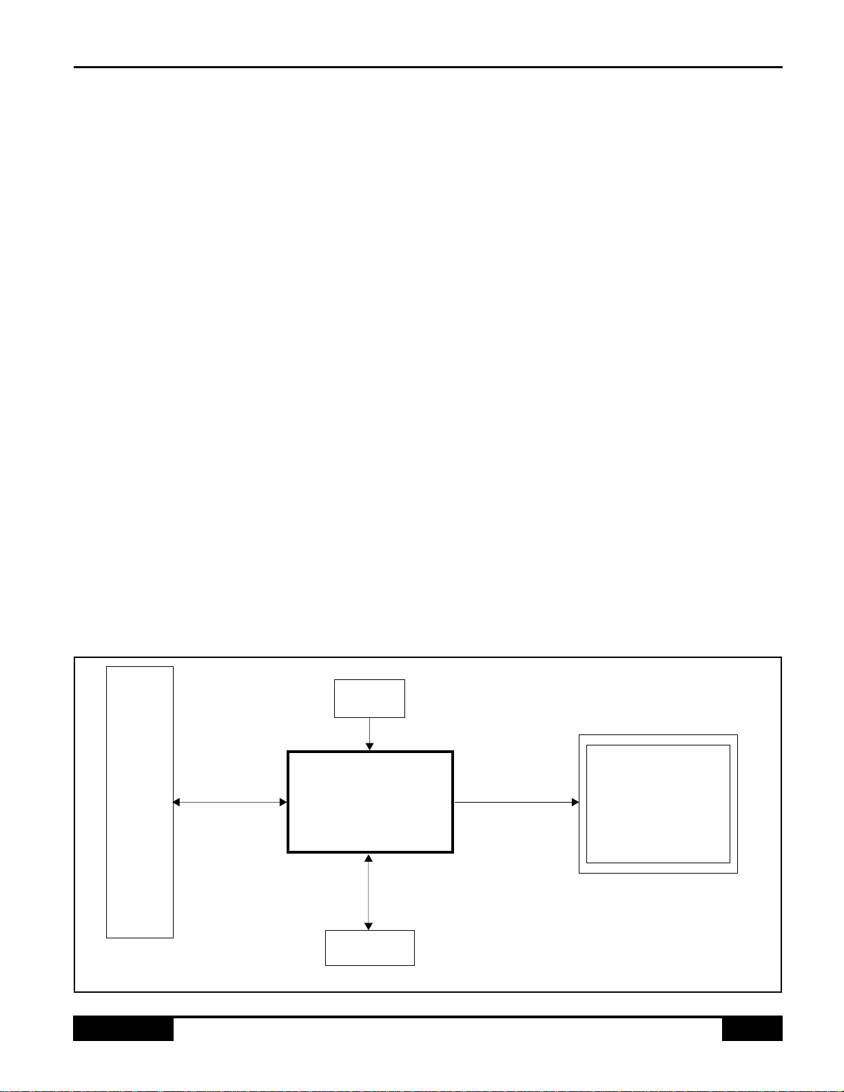
SYSTEM BLOCK DIAGRAM
MONOCHROME
ISA SPC8104
DRAM
CLOCK
BUS LCD PANEL

Data Sheet SPC8104
412-1.0
DS-4
S-MOS Systems, Inc. • Tel: (408) 922-0200 • Fax: (408) 922-0238 • http://www.smos.com
■
INTERFACE OPTIONS
Note: Example implementation, actual may vary.
-REFRESH
SA[16:0]
SD[15:0]
AEN
-IOR
-IOW
IRQ2
-SMEMR
-SMEMW
LA[23:17]
BALE
-SBHE
-MEMCS16
-IOCS16
IOCHRDY
RESETDRV
16-BIT
ISA BUS MEMEN
READY
RESET
A[16:0]
D[15:0]
IOEN#
IOR#
IOW#
MEMR#
MEMW#
IRQ
LA[23:17]
ALE
BHE#
MEMCS16#
IOCS16#
YD
LP
XSCL
LCDPWR#
WF
UD[3:0]
LD[3:0]
CLKI MD[15:0]
WE#
UCAS#
LCAS#
RAS#
MA[9:0]
SPC8104
SUSPEND#
DOZE#
PDCLK
SUSPEND#
32kHz
50%duty
DOZE#
LCD/MIM PANEL
DISPLAY
YD
LP
WF
XSCL
UD[3:0]
LD[3:0]
LCDPWR#
D[0:15]
WE#
UCAS#
RAS#
OE#
256Kx16 DRAM
LCAS#
A[9:0]
28MHz
50%duty xtal/clock
412-1.0
SPC8104 Data Sheet
DS-5
S-MOS Systems, Inc. • Tel: (408) 922-0200 • Fax: (408) 922-0238 • http://www.smos.com
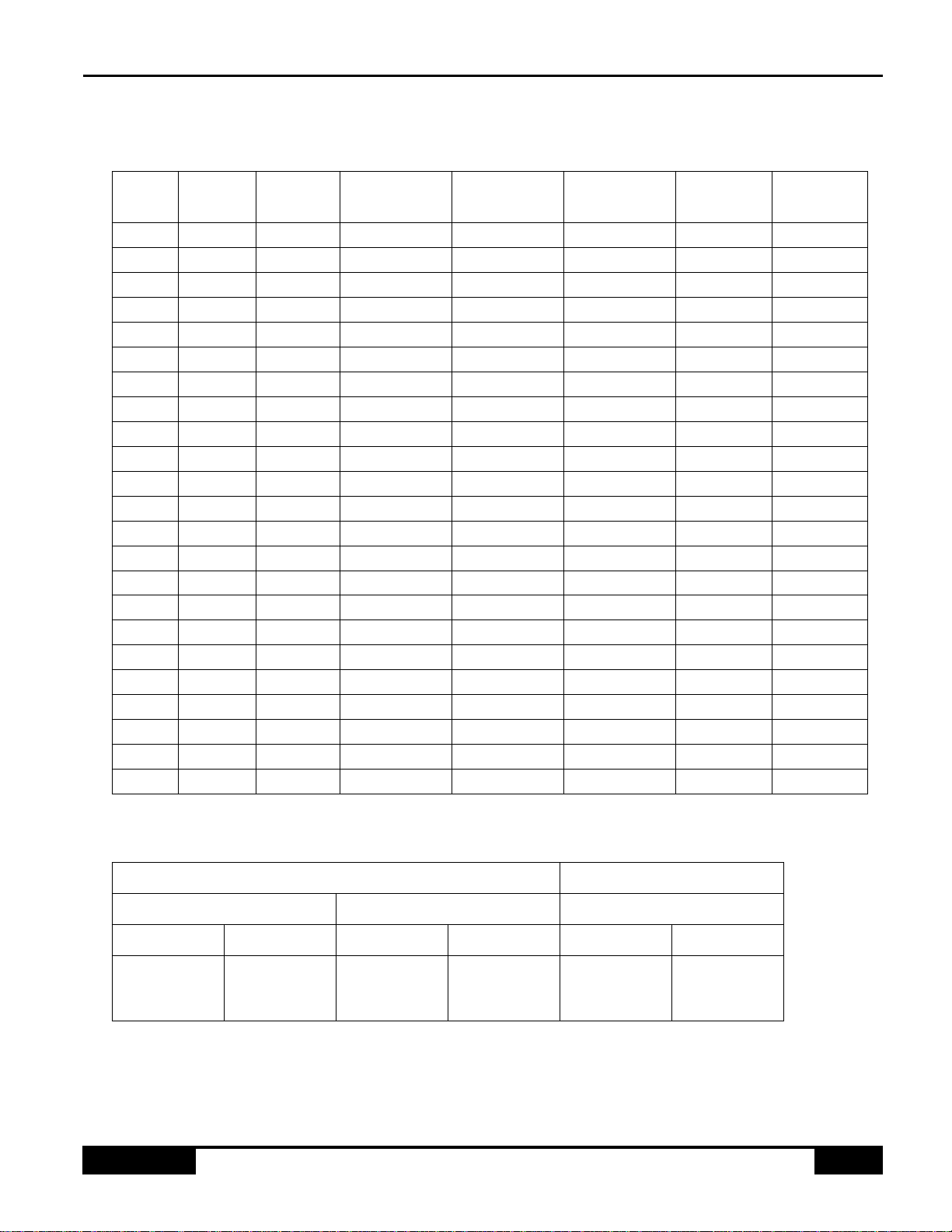
■
SUPPORTED RESOLUTIONS
■
SUPPORTED LCD INTERFACES
Mode
No. Mode
Type Font Characters Resolution Displayed
Pixels Gray
Shades Memory
Segment
0 T 8 x 8 40 x 25 320 x 200 640x400 16 B800
0+ T 8 x 14 40 x 25 320 x 350 640x350 16 B800
0++ T 8 x 16 40 x 25 320 x 400 640x400 16 B800
1 T 8 x 8 40 x 25 320 x 200 640x400 16 B800
1+ T 8 x 14 40 x 25 320 x 350 640x350 16 B800
1++ T 8 x 16 40 x 25 320 x 400 640x400 16 B800
2 T 8 x 8 80 x 25 640 x 200 640x400 16 B800
2+ T 8 x 14 80 x 25 640 x 350 640x350 16 B800
2++ T 8 x 16 80 x 25 640 x 400 640x400 16 B800
3 T 8 x 8 80 x 25 640 x 200 640x400 16 B800
3+ T 8 x 14 80 x 25 640 x 350 640x350 16 B800
3++ T 8 x 16 80 x 25 640 x 400 640x400 16 B800
4 G N/A N/A 320 x 200 640x400 4 B800
5 G N/A N/A 320 x 200 640x400 4 B800
6 G N/A N/A 640 x 200 640x400 2 B800
7 T 8 x 14 80 x 25 640 x 350 640x350 2 B000
7+ T 8 x 16 80 x 25 640 x 400 640x400 2 B000
0D G N/A N/A 320 x 200 640x400 16 A000
0E G N/A N/A 640 x 200 640x400 16 A000
0F G N/A N/A 640 x 350 640x350 2 A000
10 G N/A N/A 640 x 350 640x350 16 A000
11 G N/A N/A 640 x 480 640x480 2 A000
12 G N/A N/A 640 x 480 640x480 16 A000
8-Bit Interface 4-Bit Interface
Dual Panel Single Panel Single Panel
Horizontal Vertical Horizontal Vertical Horizontal Vertical
1
to
640
241
to
480
1
to
640
1
to
480
1
to
640
1
to
480
Data Sheet SPC8104
412-1.0
DS-6
S-MOS Systems, Inc. • Tel: (408) 922-0200 • Fax: (408) 922-0238 • http://www.smos.com
■
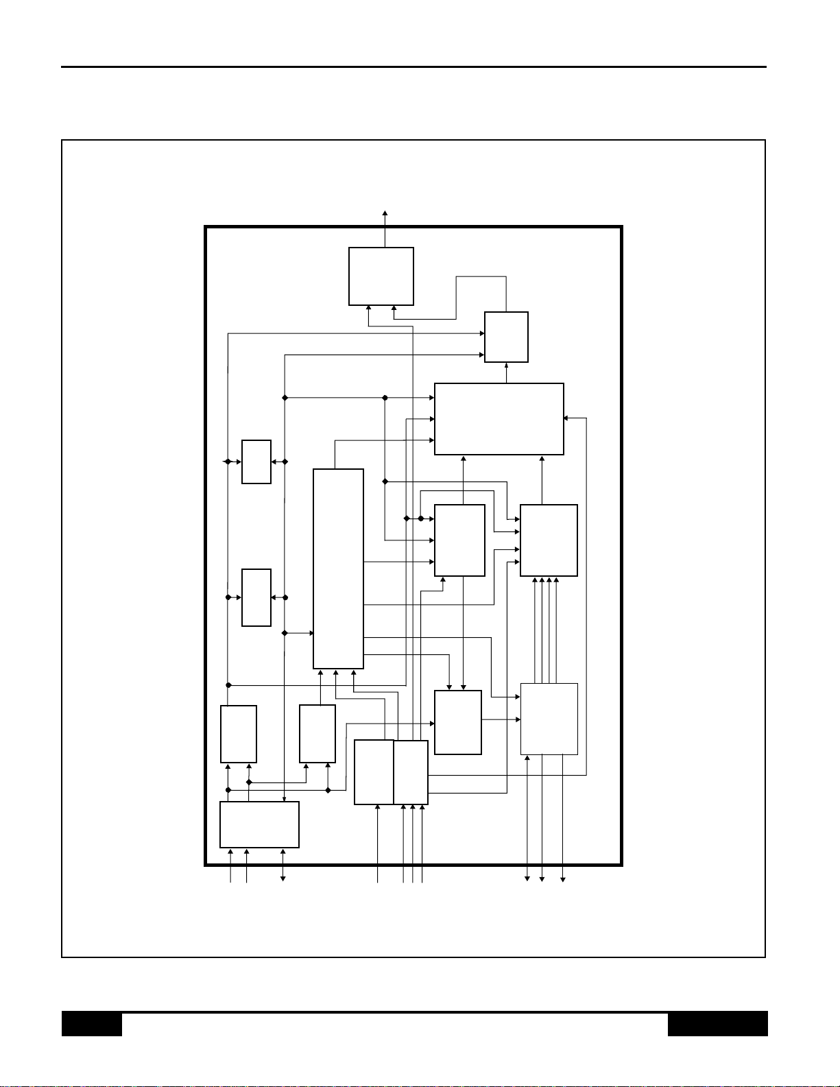
FUNCTIONAL BLOCK DIAGRAM
UD[3:0]
LD[3:0]
XSCL
LP
YD
WF
LCDPWR#
Port
Decoder Auxiliary
Ports VGA
Ports
Clock
Generator/
Divider
Sequencer
Memory
Decoder
Display
Memory
Address
Generator
CRT
Controller
Graphics
Controller
Attributes
Controller Look-Up
Table
LCD/MIM
Panel
Interface
Display
Memory
Interface
A[23:0]
D[15:0]
CLKI
MD[15:0]
MA[9:0]
DRAM
Control
16-Bit Bus
Control
Map0
Map3
Power
Save
DOZE#
PDCLK
Bus
Interface
SUSPEND#

412-1.0
SPC8104 Data Sheet
DS-7
S-MOS Systems, Inc. • Tel: (408) 922-0200 • Fax: (408) 922-0238 • http://www.smos.com
■
FUNCTIONAL BLOCK DESCRIPTION
Bus Interface
The Bus Interface is a bridge by which the chip
communicates with the CPU bus.It supports a
16-bit ISA bus.
Port Decoder
The Port Decoder decodes CPU-bus I/O cycles to pro-
vide enable and write strobes for the on-chip I/O regis-
ters.
Memory Decoder
The Memory Decoder monitors the CPU-bus activity and
decodes cycles for the display DRAM.It supplies mem-
ory access control signals to the Sequencer.
Display Memory Address Generator
The Address Generator takes the display and refresh
addresses from the CRT Controller and converts them
into RAS and CAS addresses for the display DRAM, and
multiplexes these display accesses with CPU memory
accesses.
Sequencer
The Sequencer generates internal signals to synchro-
nize the operation of the chip as well as the signals to
control the timing of the display DRAM.The Sequencer
also arbitrates between CPU and video display accesses
to the DRAM.It contains registers that allows selection of
character font set, control the structure of the video
memory and allow write masking of the individual plane
of memory.
Display Memory Interface
The Display Memory Interface is a bridge by which the
chip communicates with the DRAM.It contains buffers
that are used to store recently fetched DRAM data.
Power Save
The Power Save block contains the logic to implement
three software and hardware controlled power down
modes.
Clock Generator/Divider
The Clock Generation contains clock dividing circuits
used by the Power Save block.
Auxiliary Ports
The Auxiliary Ports are I/O registers used to control func-
tions of the chip beyond the basic VGA register set. Reg-
isters are included for controlling the LCD interface
circuits as well as the power save modes.
CRT Controller
The CRT Controller generates the horizontal and vertical
synchronization signals for the single panel or dual panel
LCD display and character and/or pixel addresses for
display data from DRAM.
Graphics Controller
The Graphics Controller supplies display memory data to
the Attributes Controller during display time and provides
data translation between the CPU bus and the display
memory during CPU read or write access cycles.
VGA Ports
The VGA Ports contain the Miscellaneous Output Status
register and the Video Subsystem Enable register used
in VGA mode.
Attributes Controller
The Attributes Controller takes in pixel and attribute infor-
mation from the Graphics Controller and display DRAM
and formats the data into pixel information which then
passes through the lookup table. It also controls display
character attributes such as blink, underline and horizon-
tal pixel panning.
Look-UpTable
The Lookup Table consists of a memory array of 64 loca-
tions of 4 bits each and hardware to convert VGA palette
writes to gray-scale values.
LCD/MIM Panel Interface
The LCD Interface block converts the display video data
from the Lookup Table into LCD display data. It also gen-
erates control signals necessary to drive single or dual-
panel LCD panels and MIM panels.For monochrome
LCD panels, the LCD interface block generates a maxi-
mum 16 gray shades through frame rate modulation and
dithering techniques.
Data Sheet SPC8104
412-1.0
DS-8
S-MOS Systems, Inc. • Tel: (408) 922-0200 • Fax: (408) 922-0238 • http://www.smos.com
■
DC SPECIFICATIONS
Absolute Maximum Ratings
Recommended Operating Conditions
Symbol Parameter Rating Units
V
DD
Supply Voltage
V
SS
-0.3 to +7.0 V
V
IN
Input Voltage
V
SS
-0.3 to V
DD
+0.3 V
V
OUT
Output Voltage
V
SS
-0.3 to V
DD
+0.3 V
T
OPR
Operating Temperature
0 to +70
°
C
T
STG Storage Temperature -65 to +150 °C
TSOL Soldering Temperature/Time 260 for 10sec max at lead °C
Symbol Parameter Condition Min Typ Max Units
HVDD Supply Voltage VSS = 0 V 3.0 3.3 3.6 V
LVDD Supply Voltage VSS = 0 V 2.25 2.5 3.6 V
VIN Input Voltage VSS VSS -- VDD V
TOPR Operating Temperature 02570˚C
IOPR Average Power Consumption VDD Core = 2.5 V
VDD IO = 3.3 V 20 mA
IPD1 Doze Mode 1 VDD Core = 2.5 V
VDD IO = 3.3 V 10 mA
IPD2 Doze Mode 2 VDD Core = 2.5 V
VDD IO = 3.3 V 55 mA
IPSUS Suspend VDD Core = 2.5 V
VDD IO = 3.3 V 0.2 mA

412-1.0
SPC8104 Data Sheet
DS-9
S-MOS Systems, Inc. • Tel: (408) 922-0200 • Fax: (408) 922-0238 • http://www.smos.com
Input Specifications
Output Specifications
Symbol Parameter Condition Min Typ Max Units
VIL Low Level Input Voltage VDD = MIN 0.8 V
VIH High Level Input Voltage VDD = MAX 2.0 V
VT+ Positive-going Threshold
(CMOS Schmitt inputs) VDD = 3.3 V 2.4 V
VT- Negative-going Threshold
(CMOS Schmitt inputs) VDD = 3.3 V 0.6 V
VHHysteresis Voltage
(CMOS Schmitt inputs) VDD = 3.3 V 0.1 V
IIZ Input Leakage Current VDD = MAX
VIH = VDD
VIL = VSS -1 1 µA
CIN Input Pin Capacitance 8 pF
RPU Pull Up Resistance VDD = 3.3 V 90 kΩ
RPD Pull Down Resistance VDD = 3.3 V 90 kΩ
Symbol Parameter Condition Min Typ Max Units
IOL1 Low Level Output Current VOL=VSS+0.4V
TS1, TS1U, CO1 3.0 mA
IOH1 High Level Output Current VOH=VDD-0.4V
TS1, TS1U, CO1 -3.0 mA
IOL2 Low Level Output Current VOL=VSS+0.4V
TS2, CO2 6.0 mA
IOH2 High Level Output Current VOH=VDD-0.4V
TS2, CO2 -6.0 mA
IOZ Output Leakage Current VOH=VDD
or VOL=VSS -1 1 µA
COUT Output Pin Capacitance 8 pF
Data Sheet SPC8104
412-1.0DS-10
S-MOS Systems, Inc. • Tel: (408) 922-0200 • Fax: (408) 922-0238 • http://www.smos.com
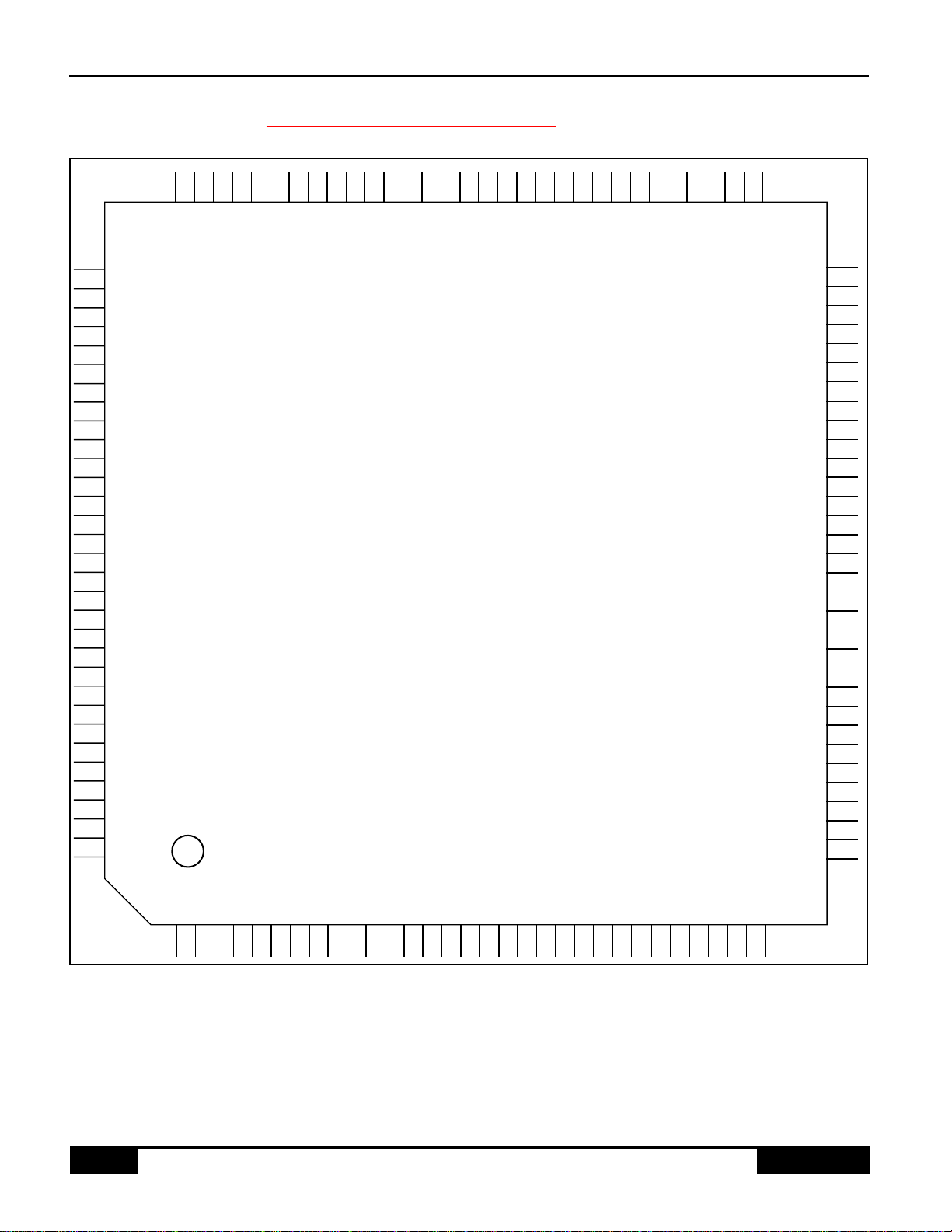
■SPC8104 PIN OUTSSOURCE: 8110_PINOUT_08.CAN
1234567891011121314151617181920212223242526272829303132
96 95 94 93 92 91 90 89 88 87 86 85 84 83 7475 73 72 71 70 69 68 67 66 6582 81 80 79 78 77 76
128
127
126
125
124
123
122
121
120
119
118
117
116
115
114
113
112
111
110
109
108
107
106
105
104
103
102
101
100
99
98
97
33
34
35
36
37
38
39
40
41
42
43
44
45
46
47
48
49
50
58
59
60
61
62
63
51
52
53
54
55
56
57
64
SPC8104
D8
D9
D10
D11
D12
D13
D15
XSCL
LP
LD0
LD1
LD2
LD3
D14
LCDPWR#
VDD I/O
VSS CORE
VDD CORE
VDD CORE
MA4
VSS I/O
WF
PDCLK
UD0
UD1
UD2
UD3
VSSCORE
VDD I/O
MA3
MA5
MA2
MA6
MA1
A3
N/C
A2
A1
A0
IOW#
MEMW#
MA7
MA0
MA8
RAS#
UCAS#
WE#
LCAS#
MD8
MD7
MD9
MD6
MD10
MD5
MD11
VSSI/O
VSSI/O
RESET
D7
D6
D5
D4
D3
D2
D1
D0
A16
A15
A14
A13
A12
A11
A10
A9
A8
A7
A6
A5
A4
VDD CORE
CLKI
SUSPEND#
MD0
MD15
MD1
MD14
MD2
MD13
MD3
MD12
IOEN#
IOR#
VSSCORE
BHE#
VDD I/O
VSS I/O
VDD I/O
VSSCORE
RDACK#
YD
TSTCO
MA9
VDD CORE
DOZE#
IRQ
VSS I/O
VDD I/O
MEMCS16#
IOCS16#
MD4
READY
MEMEN
VSSCLKI
VDD CLKI
VSS I/O
MEMR#
VDD I/O
VSS CORE
VDD CORE
LA20
LA23
LA22
LA19
LA18
LA17
LA21
ALE
TSTEN

412-1.0
SPC8104 Data Sheet
DS-11
S-MOS Systems, Inc. • Tel: (408) 922-0200 • Fax: (408) 922-0238 • http://www.smos.com
■PIN DESCRIPTION
Key
CPU Interface
A = Analog
I = Input
O = Output
I/O = Bidirectional
P=Power
Pin Name Type Pin # Description
A[0:16],
LA[17:23] I 100~106,
109~116,
119~127
CPU bus unlatched address inputs. For an 8-bit CPU interface configuration,
LA[20:23] are ignored and LA[17:19] should be connected to the latched CPU
address SA[17:19]. In Suspend Mode, the Address inputs are internally masked off.
D[0:15] I/O 2~10,
13~19 16 bit ISA-Bus data bus. These lines are driven by the chip only during read cycles,
and are in a hi-Z state at all other times. In Suspend Mode, these inputs are
internally masked off.
ALE I 99 ISA Bus Address Latch Enable. ALE is ignored for an 8-bit CPU interface
configuration. In Suspend Mode the this input is disabled.
MEMEN I 92 ISA Bus Memory Enable. This signal should be connected to the -REFRESH signal
on the ISA bus. When this signal is low (e.g. during a system memory refresh
cycle), memory address decoding is disabled.
IOR# I 94 ISA Bus I/O Read Strobe. In Suspend Mode the this input is disabled.
IOW# I 93 ISA Bus I/O Write Strobe. In Suspend Mode the this input is disabled.
MEMR# I 91 ISA Bus Memory Read Strobe. In Suspend Mode the this input is disabled.
MEMW# I 90 ISA Bus Memory Write Strobe. In Suspend Mode the this input is disabled.
IOEN# I 95 ISA Bus I/O Enable. This input should be connected to the ISA bus AEN signal.
When this signal is high, I/O address decoding is disabled. In Suspend Mode the
this input is disabled.
READY O 89 ISA Bus READY signal. This output is driven low to force the CPU to insert wait
states during memory cycles. READY is released to high-Z after a transfer is
complete.
RESET I 84 The active high Reset signal from the CPU clears all internal registers and forces all
signals to their inactive state. During Suspend Mode the RESET input is ignored.
IRQ O 83 ISA Bus Vertical Interrupt. When enabled, a Vertical Retrace Interrupt will cause
this signal to be driven from a logic 0 state to a logic 1 (rising-edge triggered
interrupt). Once set, this interrupt must be cleared by a bit in the CRTC registers. A
control bit in the Auxiliary Registers allows this output to be optionally disabled (tri-
stated).
MEMCS16# O 87 ISA Bus Memory Chip Select 16. Address inputs LA[23:17] are decoded to drive
this output low when a valid memory address (AXXXXh, BXXXXh) appears on the
bus.
IOCS16# O 88 ISA Bus I/O chip Select 16. Address inputs A[15:0] and IOEN# are decoded to drive
this output low when a valid SPC8104 I/O register address appears on the bus.
Note that I/O addresses 3C6h-3C9h does not result in IOCS16# being driven low
(i.e. internal LUT register reads and writes are 8 bit cycles).
BHE# I 98 ISA Bus Byte High Enable. In Suspend Mode the this input is disabled.
RDACK# O 20 Read Acknowledge. This pin goes low during valid I/O or memory reads to the chip.

Data Sheet SPC8104
412-1.0DS-12
S-MOS Systems, Inc. • Tel: (408) 922-0200 • Fax: (408) 922-0238 • http://www.smos.com
Frame Buffer Memory Interface
Clock Inputs
Power Supply
Pin Name Type Pin # Description
MA[0:9] O 48, 46,
42, 40,
39, 41,
45, 47,
49, 50
Multiplexed row/column address bits for video display memory.
MD[0:4]
MD[7:15]
I/O 74, 72,
70, 68,
66, 58,
57, 59,
61, 63,
67, 69,
71, 73
Data bits for video display memory. The output drivers of these pins are placed into a
high-impedance state when RESET is high. On the falling edge of RESET, the
values on MD[3:0] are latched into a read-only Auxiliary Register and are available to
be read as configuration inputs. Also, the values on MD[5:6] are used to configure
other various hardware options - see Section 5.8, Summary of Configuration
Options, for details. Note that there are internal pullup resistors on the inputs of
these pins except MD[5:6].
MD[5:6] I/O 62, 60
RAS# O 51 DRAM Row Address Strobe.
LCAS#
(LWE#) O 56 DRAM Column Address Strobe for low byte (LCAS#), or Write Enable Strobe for low
byte (LWE#), as determined by logic value on MD[6] during RESET (see pin
mapping table).
UCAS#
(CAS#) O 52 DRAM Column Address Strobe for high byte (UCAS#), or single Column Address
Strobe (CAS#), as determined by logic value on MD[6] during RESET (see pin
mapping table).
WE#
(UWE#) O 53 DRAM Write Enable Strobe (WE#), or Write Enable Strobe for high byte (UWE#), as
determined by logic value on MD[6] during RESET (see pin mapping table).
Pin Name Type Pin # Description
CLKI I 77 This is the clock source input and should be connected to an external oscillator.
Pin Name Type Pin # Description
VDD CORE P 12, 33, 55, 97, 118 VDD supply for core logic.
VDD I/O P 1, 22, 44, 65, 86,
108 VDD supply for I/O pins.
VDD CLKI P 76 VDD supply for CLKI pin.
VSS CORE P 11, 32, 54, 96, 117 VSS supply for core logic.
VSS I/O P 21, 43, 64, 85,
107, 128 VSS supply for I/O pins.
VSS CLKI P 75 VSS supply for CLKI pin.
412-1.0
SPC8104 Data Sheet
DS-13
S-MOS Systems, Inc. • Tel: (408) 922-0200 • Fax: (408) 922-0238 • http://www.smos.com
Test Function
LCD Panel Interface
Pin Name Type Pin # Drv Description
TSTCO I 38 CD This pin enables the chip’s test mode for the core logic. This pin must
always be unconnected or tied to ground.
TSTEN I 82 CD This pin enables the chip’s test mode for the I/O cells. This pin must
always be unconnected or tied to ground.
N/C 78 No Connection
Pin Name Type Pin # Description
YD O 25 Vertical Scanning Start Pulse output. A logic 1 on this signal, sampled by the LCD/
MIM panel module on the falling edge of LP, is used by the panel row drivers (Y
drivers) to indicate the start of the vertical frame.
LP O 26 Latch Pulse output. The falling edge of this signal is used to latch a row of display
data in the LCD/MIM panel module’s column driver shift registers and to turn on the
row driver (Y driver) for that line.
XSCL O 23 Shift Clock for LCD panel data or Pixel Clock for MIM panel data. Display data is
clocked out of the chip on the rising edge of this signal, to be shifted into the LCD/
MIM panel module column drivers (X drivers) on each falling edge.
UD[0:3] O 34~37 Upper panel display data for dual LCD panel mode. For single LCD panel mode,
these bits are the most significant 4 bits of the 8 bit output data to the panel
(PD[4:7]). For 4-bit single LCD panel mode, these bits are the 4 bits of output data
to the panel. For 4-bit MIM panel mode, these bits are driven 0.
LD[0:3] O 28~31 Lower panel display data for dual LCD panel mode. For 8-bit single LCD panel
mode, these bits are the least significant 4 bits of the 8 bit output data to the panel
(PD[0:3]). For 4-bit single LCD panels, these bits are driven 0. For 4-bit MIM panel
mode, these are the 4 bits of output data to the panel.
LCDPWR# O 27 LCD power control. In normal operation this signal is driven low to enable an
external LCD power supply. This signal is driven high when the chip is put into any
power save mode, or if the Sequencer is in a reset state. It can be used externally
to turn off the panel supply voltage and backlight. After a RESET, this signal is held
high until the CRTC is programmed and running.
WF O 24 LCD Panel Backplane Bias Signal or MIM Panel Data Enable Signal. In LCD panel
mode, the WF signal toggles once per vertical frame period. In MIM panel mode,
this signal goes high whenever display data are valid.
Data Sheet SPC8104
412-1.0DS-14
S-MOS Systems, Inc. • Tel: (408) 922-0200 • Fax: (408) 922-0238 • http://www.smos.com
Power Save Mode Control
Configuration Options
Multiple Function Pin Descriptions
MixedVoltage Configurations
Pin Name Type Pin # Description
PDCLK I 79 Power Down Clock. This input may be used to provide a low frequency clock for
generating DRAM refresh in Suspend mode, as an optional alternative to using the
pixel clock or MEMEN input as the DRAM refresh clock source. This clock input
should be driven by a 32 kHz 50% duty cycle clock. The PDCLK input is used to
directly generate the RAS and CAS pulses in Suspend mode.
SUSPEND# I 80 A low level on this pin puts the chip into the hardware Suspend mode. The
SUSPEND# signal overrides any software initiated power save modes as well as
the DOZE# input pin, and disables the CPU bus interface inputs. CPU Address and
Data inputs are masked when this signal is low. When in Suspend Mode the
UD[3:0], LD[3:0], XSCL, LP, YD and WF signals are driven into a low state (or
optionally, a high impedance state) and the LCDPWR# signal is driven high.
DOZE# I 81 A low level on this pin puts the chip into Doze mode. The function of the Doze mode
is determined by the Doze Mode Select bits in AUX[03]. This pin is ignored if the
SUSPEND# input pin is asserted.
Pin Name value on this pin at falling edge of RESET is used to configure: (1/0)
MD[3:0] values latched into read-only AUX[0C] bits 7-4 for software use
MD[5] LCD signals’ state in Suspend mode: Low (1), or Hi-Z (0)
MD[6] 2 CAS, 1 WE type DRAM (1), or 1 CAS, 2 WE type DRAM (0)
Pin Name Function MD Line Status Functional Description
LCAS#, LWE# LCAS# MD[6] = 1 DRAM Column Address
Strobe (Low Byte)
LWE# MD[6] = 0 DRAM Write Enable Strobe
UCAS#, CAS# UCAS# MD[6] = 1 DRAM Column Address
Strobe (High Byte)
CAS# MD[6] = 0 DRAM Column Address Strobe
WE#, UWE# WE# MD[6] = 1 DRAM Write Strobe
UWE# MD[6] = 0 DRAM Write Strobe
(High Byte)
CoreVDD I/O VDD
2.5V 3.3 V
2.5V No Yes
3.3V No Yes
Table of contents


