Seiko Epson E0C5251 User manual

MF1329-01
CMOS CALLING NUMBER IDENTIFICATION RECEIVER IC E0C5251
TECHNICAL MANUAL

NOTICE
No part of this material may be reproduced or duplicated in any form or by any means without the written
permission of Seiko Epson. Seiko Epson reserves the right to make changes to this material without notice.
Seiko Epson does not assume any liability of any kind arising out of any inaccuracies contained in this material
or due to its application or use in any product or circuit and, further, there is no representation that this material
is applicable to products requiring high level reliability, such as medical products. Moreover, no license to any
intellectual property rights is granted by implication or otherwise, and there is no representation or warranty that
anything made in accordance with this material will be free from any patent or copyright infringement of a third
party. This material or portions thereof may contain technology or the subject relating to strategic products under
the control of the Foreign Exchange and Foreign Trade Law of Japan and may require an export license from
the Ministry of International Trade and Industry or other approval from another government agency.
All the product names mentioned herein are trademarks and/or registered trademarks of their respective owners.
© SEIKO EPSON CORPORATION 2000 All ri
g
hts reserved.

CONTENTS
E0C5251 TECHNICAL MANUAL EPSON i
CONTENTS
1 Overview.......................................................................................................................1
1.1 Features......................................................................................................................................................................1
1.2 Block Diagram...........................................................................................................................................................2
1.3 Pin Assignment.........................................................................................................................................................2
1.4 Pin Description..........................................................................................................................................................3
2 Power Supply Block and Initial Reset...........................................................................6
2.1 Power Supply............................................................................................................................................................6
2.2 Initial Reset.................................................................................................................................................................6
3 Functional Description..................................................................................................7
3.1 Register Description................................................................................................................................................7
3.2 Outputs from the #RDET, #IRQ and #DET Pins.......................................................................................12
3.3 Input Amp Circuit...................................................................................................................................................13
3.3.1 Differential Input..................................................................................................................................13
3.3.2 Single End Input.................................................................................................................................14
3.4 Ring/Line Reversal Signal Detection.............................................................................................................15
3.5 FSK Demodulation...............................................................................................................................................15
3.6 Dual-Tone Detection............................................................................................................................................16
3.7 Off-Hook Detection...............................................................................................................................................16
4 Precautions on Mounting............................................................................................17
5 Electrical Characteristics............................................................................................19
5.1 Absolute Maximum Ratings..............................................................................................................................19
5.2 Recommended Operating Conditions...........................................................................................................19
5.3 DC Characteristics................................................................................................................................................19
5.4 Current Consumption...........................................................................................................................................19
5.5 Crystal Oscillation Characteristics...................................................................................................................20
5.6 FSK Demodulation Circuit Characteristics...................................................................................................20
5.6.1 FSK AC Characteristics....................................................................................................................20
5.6.2 FSK Switching Characteristics.......................................................................................................20
5.6.3 FSK Energy Detection Mode AC Characteristics...................................................................21
5.6.4 FSK Energy Detection Mode Switching Characteristics......................................................21
5.7 Dual-Tone (CAS) Detection Circuit Characteristics.................................................................................22
5.7.1 CAS AC Characteristics...................................................................................................................22
5.7.2 CAS Switching Characteristics......................................................................................................22
5.8 Call Progress Mode (CPM) Detection Circuit Characteristics..............................................................23
5.8.1 CPM AC Characteristics...................................................................................................................23
5.8.2 CPM Switching Characteristics......................................................................................................23
5.9 Serial Interface Circuit Characteristics..........................................................................................................24
5.9.1 Serial Interface AC Characteristics..............................................................................................24
5.9.2 FSK Demodulated Data Read Mode..........................................................................................25
5.9.3 CAS Detection Circuit Control-Register Write Mode.............................................................25
5.10 E0C5251 Timing Chart.....................................................................................................................................26
5.10.1 Bellcore On-Hook Data Transfer................................................................................................26
5.10.2 Bellcore Off-Hook Data Transfer................................................................................................26
5.10.3 BT Idle State CLI Service.............................................................................................................27
5.10.4 BT Loop State CLI Service..........................................................................................................27

CONTENTS
ii EPSON E0C5251 TECHNICAL MANUAL
5.11 External Wiring Diagram (Example)............................................................................................................28
5.11.1 Example of Bellcore-Compatible Telephone Circuit...........................................................28
5.11.2 Example of Bellcore-Compatible Auxiliary Circuit................................................................29
6 Package......................................................................................................................30
7 Pad Layout..................................................................................................................31
7.1 Pad Layout Diagram............................................................................................................................................31
7.2 Pad Coordinates...................................................................................................................................................31

1 OVERVIEW
E0C5251 TECHNICAL MANUAL EPSON 1
1 Overview
The E0C5251 (CAS + FSK IC), an upgraded version of the E0C5250, is a CMOS IC for calling number
identification with the Call Waiting function.
It provides an interface to various call information delivery services based on Bellcore GR-30-CORE, such as CND
(Calling Number Delivery), CNAM (Calling Name Delivery), and CIDCW (Calling Identity on Call Waiting), as
well as British Telecom’s CLIP (Calling Line Identification Service)andCableCommunicationsAssociation’sCDS
(Caller Display Service).
The E0C5251 incorporates power-down, ring detection, and carrier detection circuits, a synchronous receive data
output function, and a clock-synchronized serial interface. All these features make itsuitableforvariousapplications
such as those listed below.
• Calling number delivery service with a Call Waiting function
• Telephone sets and similar auxiliary equipment
• Telephone answering equipment
• Multifunction telephones
• Facsimiles
• Computer peripheral circuits
• Message waiting telephones
1.1 Features
• Conforms to Bellcore GR-30-CORE and SR-TSV-002476 (same as E0C5250)
• Conforms to British Telecom SIN227 and SIN242 (same as E0C5250)
• Can detect Bellcore CPE alert signal (CAS) and British Telecom idle-tone alert signal using a programmable
band-pass filter (same as E0C5250)
• FSK demodulation circuit based on ITU-T V.23 and BELL202 (same as E0C5250)
• Filter bypass mode to detect call progress mode (CPM) signal (same as E0C5250)
• Programmable alert-signal detection level (same as E0C5250)
• Carrier/ring detection output (same as E0C5250)
• FSK energy mode to detect FSK signal in power-down mode (new function for E0C5251)
• Supports CAS signal single-end input (new function for E0C5251)
• Off-hook detection (new function for E0C5251)
• Supports 3.57945 MHz crystal oscillator or external clock input (same as E0C5250)
• Serial-receive data output (same as E0C5250)
• Serial host interface (same as E0C5250)
• Power-down mode (same as E0C5250)
• Power supply voltage: 2.7 V to 5.5 V (same as E0C5250)
• Operating temperature range: -20°C to 70°C (same as E0C5250)
• Current consumption: 3 mA when operating (same as E0C5250)
1 µA in zero-power mode (same as E0C5250)
6 µA in FSK energy detection mode (new function for E0C5251)
• Shipping form: SOP2-28pin package (plastic), DIP-28pin package (ceramic) or chip (package for E0C5251)

1 OVERVIEW
2EPSON E0C5251 TECHNICAL MANUAL
1.2 Block Diagram
Band-pass
filter
CAS tone
filter
INN SDO
#DET
#PQUAL
Amp
–
+
INP
BPOUT
OSC3EXTCLK OSC4
EXTREF
–
+
HOOK
CASIN Amp
–
+
CASFB
FB
RDIN
V
DD
V
SS
#RDET V
DD
V
REF
V
DD
/2
(MODE0 ∗SEL)
(MODE1)
FSK
demodulator
Identification
circuit
CDIN
PDWN #RESET MODE1MODE0
Data/timing
recovery
circuit
Detection
circuit
Timing generator Control circuit
Interrupt
control circuit
#IRQ
SDI
#SCLK
#RDRC
To other blocks
Amp( )
Figure 1.2.1 Block diagram
1.3 Pin Assignment
SOP2-28pin DIP-28pin
1
14
28
15
E0C5251
28
15
1
14
E0C5251
No. Pin name No. Pin name No. Pin name No. Pin name
1 INP 8 HOOK 15 OSC3 22 #IRQ
2 INN 9 RDIN 16 OSC4 23 #SCLK
3 FB 10 #RDRC 17 EXTCLK 24 SDI
4 CASIN 11 #RDET 18 MODE0 25 SDO
5 CASFB 12 PDWN 19 MODE1 26 CDIN
6VREF 13 #RESET 20 #PQUAL 27 BPOUT
7 EXTREF 14 VSS 21 #DET 28 VDD
Figure 1.3.1 Pin assignment

1 OVERVIEW
E0C5251 TECHNICAL MANUAL EPSON 3
1.4 Pin Description
Note: The signal and pin names prefixed by # in this manual are those of active-low signals and pins.
Table 1.4.1 Pin description
Pin name Pin No. Type Power-down
status Description
INP 1 Input
Analog Off/
Active + Input: Non-inverting amplifier input. This pin is connected to the
telephone wire through an input gain-setting resistor and a DC cut
capacitor. Under the power downmode, this pin is functionary
disconnected from the internal circuitry when the MODE1 pin is set to
low level. When the MODE1 pin is set to high level, this pin stays
active to detect FSK signal energy to send wake up signal to the host
through the #IRQ pin. Do not connect any external components to this
pin except gain setting resistors to this pin. Excess load may cause
improper operation of the circuit.
INN 2 Input
Analog Off/
Active - Input: Inverting amplifier input. This pin is connected to the
telephone wire through an input gain-setting resistor and a DC cut
capacitor. Under the power downmode, this pin is functionary
disconnected from the internal circuitry when the MODE1 pin is set to
low level. When the MODE1 pin is set to high level, this pin stays
active to detect FSK signal energy to send wake up signal to the host
through the #IRQ pin. Do not connect any external components to this
pin except gain setting resistors to this pin. Excess load may cause
improper operation of the circuit.
FB 3 Output
Analog High-Z/
Active Amplifier Output: A feed back resistor is connected between this pin
and the INN pin to set gain. Under the power downmode, this output
pin is set to high impedance when the MODE1 pin is set to low level.
When theMODE1 pin is set to high level in power down, this pinstays
active to detect FSK signal energy to send wake up signal to the host
through the #DET pin. Do not connect any external components to
this pin except a gain setting resistor to this pin. Excess load may
cause improper operation of the circuit.
CASIN 4 Input
Analog Off CAS Tone Input: CAS tone amplifier input. For the telephone
application, this pin is connected to the output of telephone hybrid
circuit through input gain-setting resistor and a DC cut capacitor.
Under the power down mode, this pin is functionary disconnected
from the internal circuitry. Do not connect any external components to
this pin except gain setting resistors to this pin. Excess load may
cause improper operation of the circuit.
CASFB 5 Output
Analog High-Z CAS Amplifier Output: A feed back resistor is connected between
this pin and the CASIN pin to set CAS gain. Under the power down
mode, this output pin is set to high impedance. Do not connect any
external components to this pin except a gain setting resistor to this
pin. Excess load may cause improper operation of the circuit.
VREF 6 Output
Analog High-Z/
VDD/2 level Reference Voltage Output: 1/2 VDD voltage output. This pin must be
bypassed to ground through 0.1 µF capacitor. During power down
mode, this output pin is set to high impedance when the MODE1 pin
is low level. When theMODE1 pin is set to high level in power down,
this pin stays at VDD/2. Do not connect any external components to
this pin except a jumper to VREF pin or a bypass capacitor to ground.
Excess load may cause improper operation of the circuit.
EXTREF 7 Input
Analog Active External Reference Voltage Input: External DC reference voltage is
connected to this pin. This voltage set the off-hook detectionthreshold
level.
HOOK 8 Input
Analog Active Off-Hook Detection Input: Diode bridge output from the TIP/RING
lines is connected to this pin through external resistor divider todetect
off-hook/on-hook states.
RDIN 9 Schmitt
trigger input Active Ring Detect Input: The attenuated ring signal is connected to thispin
for the ring detection. This circuit is always active even if the device is
in the power down mode.

1 OVERVIEW
4EPSON E0C5251 TECHNICAL MANUAL
Pin name Pin No. Type Power-down
status Description
#RDRC 10 Open-drain
output
Schmitt
trigger input
Active Ring Detect RC Terminal: RC network will be connected to this pin
to set time delays for the ring signal detection. This circuit is always
active even if the device is in the power down mode.
#RDET 11 Output Active Ring Detect Output: When theMODE1 pin is set to low level,thispin
is connected from output of a Schmitt trigger buffer which input is
connected to the#RDRC pin. Low level at this pin indicates that the
ring signal is detected. When theMODE1 pin bit is set to high level,
this pin is connected from outputof a hook detect circuit whichinput is
connected from the HOOK pin. High level at this pinindicateson-hook
condition and low level at this pin indicates off-hook condition.
PDWN 12 Input Active Power Down Input: This pin must be kept at low level for the normal
operation. When it is set to high level, the device enters the power
down mode. During power down mode, the OSC4 pin is set to high
level, and the VREF, CASFB and FB pins are set to high impedance.
(The FB and VREF pins are set to high impedance only when the
MODE1 pin is at low level.)
#RESET 13 Input Active Reset Input: When this pin is set to low level, all internalhost
registers are reset to their default conditions.This pin must be set to
high level to write data to the internal registers.
VSS 14 Power
supply (-) Device Ground: This pin is connected to the system ground.
OSC3 15 Input Off Crystal Oscillator/External Clock Input: A crystal resonator is
connected between this pin and the OSC4 pin. This pin may be driven
from an external clock source. The proper value load capacitor must
be connected between this pin and ground. During power down, this
input pin is disconnected from internal circuits.
OSC4 16 Output High level Crystal Oscillator Output: A crystal or ceramic resonator is
connected betweenthis pin and OSC3 pin. This pin must be kept
open when the OSC3 pin is driven from an external clock source.The
proper value load capacitor must be connected between this pin and
ground. During power down, this output pin is set to high level.
EXTCLK 17 Input Active External Clock Input: Typically 32.768 kHz clock signal is applied to
this pin from the host device to enable pre-qualification logicused in
FSK energy detection circuitry.
MODE0 18 Input Active Mode0 Select Input: This pin select CAS or FSK/CPM mode. When
this pin is set to high level, CAS mode is selected. In this mode, CAS
detection is enabled and the FSK function is disabled. Thehostdevice
also can write internal registers through the SDI and #SCLK pin.
Before writing data into registers, this pin must be set to low levelonce
to synchronize the serial interface circuit for data writing sequence.
When this pin is set to low level, FSK/CPM mode is selected. In this
mode, CAS detection is disabled and the FSK/CPM function is
enabled. The host device also can read the received data from the
SDO pin under this mode.Refer to Table 3.2.1 for more details.
MODE1 19 Input Active Mode1 Select Input: This pin enables FSK energy and off-hook
detection mode. When this pin is set to high level, FSK energy and
off-hook detection mode is enabled. When this pin is set to low level,
FSK energy and off-hook detection mode is disabled. Refer to Table
3.2.1 for more details.
#PQUAL 20 Output High level Pre-qualification Output: Early qualification output will be monitored
at this pin. When no tones are detected, this pin stays at high level.

1 OVERVIEW
E0C5251 TECHNICAL MANUAL EPSON 5
Pin name Pin No. Type Power-down
status Description
#DET 21 Output Active Detection Output: When the device is in the power down mode and
the MODE1 pin is set to low level, low level at this pin indicates the
presence of ring signal or phoneline reversal. If the MODE1 pin is set
to high level, low level at this pin indicates the presence of ring signal
or FSK inbound signal. When in the power up mode and FSK mode is
selected, low level at this pin indicates the presence of FSK inbound
signal. If CPM mode is selected, pulses from this pin indicate the
presence of CPM tone signal. If CAS mode is selected, low level at
this pin indicates the presence of CAS tone signal. Refer to Table
3.2.1 for more details.
#IRQ 22 Open-drain
output Active Interrupt Request Output: When the device is in the power down
mode, low level at this pin indicates the presence of ring signal or
phone line reversal. When in the power up mode and FSK mode is
selected, low level at this pin indicates that the receiveddata is ready
in the internal register for the host device to read. In this mode, thispin
is set to high level after the first bit of the receiveddata is read. IfCPM
mode is selected, low level at this pin indicates the presence of CPM.
If CAS mode is selected, low level at this pin indicates that the CAS
tone is detected. In this mode, this pin remains low level while CAS
tones exist. Refer to Table 3.2.1 for more details.
#SCLK 23 Input Active Serial Clock Input: The host device supplies a clock to this pin to
write internal registers or to read received data. The received data
changes its state at falling edge of the clock supplied by the host
device.
SDI 24 Input Active Serial Data Input: The host device writes control bits through this pin.
SDO 25 Output High level Serial Data Output: The host device reads the serial receive data
from this pin. If asynchronous mode is selected, the asynchronous
format serial data appears at this pin. If synchronous mode is
selected, the received serial data is read from this pin by the host
device with the serial clock supplied to the #SCLK pin. During the
power down, CPM or CAS mode, this output pin is set to high level.
CDIN 26 Input
Analog VREF Capacitor Input: A 0.1 µF capacitor is connected between this pin
and the BPOUT pin. The FSK signal can be applied from the FBpin
to this pin through this 0.1 µF capacitor to bypass the band pass filter
for internal testing purpose. Do not connect any external components
except this capacitor to this pin. Excess load may cause improper
operation of the circuit.
BPOUT 27 Output
Analog High-Z Capacitor Output: A 0.1 µF capacitor is connected between this pin
and the CDIN pin. The band pass filter output is monitored at this pin
for internal testing purpose. Do not connect any external components
except this capacitor to this pin. Excess load may cause improper
operation of the circuit.
VDD 28 Power
supply (+) Device Power Supply: Positive power supply pin.
2 POWER SUPPLY BLOCK AND INITIAL RESET
6EPSON E0C5251 TECHNICAL MANUAL
2 Power Supply Block and Initial Reset
2.1 Power Supply
The following shows the operating power supply voltage of the E0C5251.
Power supply voltage: 2.7 V to 5.5 V
The E0C5251 is operated in the above voltage range by a single power supply that is connected between VDD and
VSS. The voltage required for internal operation (VREF = 1/2 VDD) is generated by the IC itself.
+
–
VDD
VREF
VSS
R
R
–
+
External
power
supply
Figure 2.1.1 Power supply block
2.2 Initial Reset
The E0C5251 contains control registers that can be accessed by the external CPU through a serial interface. The
control registers are initialized by an initial reset which is applied from the #RESET pin.
#RESET
MODE0
Control register
RWrite control circuit
R
Figure 2.2.1 Initial reset circuit
Specifically, the control registers are reset by pulling the #RESET pin to Low level (VSS) from outside of the IC.
Then, the reset state is eliminated by releasing the #RESET pin back to High level (VDD). Also, the write control
circuit for the control register is reset when the #RESET pin or MODE0 pin is at Low level. Before data can be
written to the control register, both #RESET and MODE0 must be at High level.

3 FUNCTIONAL DESCRIPTION
E0C5251 TECHNICAL MANUAL EPSON 7
3 Functional Description
3.1 Register Description
The E0C5251 contains eight 4-bit registers that can be accessed by the CPU.
The CPU can access these CPU interface registers through the serial interface pins (SDI, #SCLK, andMODE0)and
control the mode of the E0C5251. The CPU uses the first four bits of transmit data to specify the address A[3:0] of
the internal register to be accessed. The data is transmitted beginning with the LSB (A0). The four bits that follow
the LSB are data bits D[3:0] which are the data to be written to the specified register. This data is also transmitted
beginning with the LSB (D0).
Table 3.1.1 shows registers and control bit assignments.
Table 3.1.1 Register structure
Register Address Initial value Data bit
name A[3:0] D3 D2 D1 D0
MDR 0000 0000 TEST SEL BT SYNC
GLR 0001 0100 GL3 GL2 GL1 GL0
GHR 0010 0100 GH3 GH2 GH1 GH0
TLR 0011 0110 TL3 TL2 TL1 TL0
THR 0100 XXX1 X X X TH0
AVR 0101 X011 X AV2 AV1 AV0
WLR 0110 0001 WL3 WL2 WL1 WL0
WHR 0111 0001 WH3 WH2 WH1 WH0

3 FUNCTIONAL DESCRIPTION
8EPSON E0C5251 TECHNICAL MANUAL
Each register is detailed below.
MDR: Mode Register (Address = 0h)
Table 3.1.2 MDR register
Bit Bit name Initial
value Description
D0 SYNC 0 Asynchronous/synchronous mode selection
This bit is used to select asynchronous or synchronous mode.
SYNCbit Mode
0 Selects asynchronous mode
1 Selects synchronous mode
Asynchronous mode is selected by setting this bit to 0, inwhich case the 8-bit
serial data output from the SDO pin is forwarded in asynchronous mode.
Synchronous mode is selected by setting this bit to 1. When theFSK signal is
received in FSK mode, serial data is output from the SDO pin and read by the
CPU synchronously with the clock signal fed from the CPU to the #SCLK pin.
Also, in synchronous mode, when the receive data is ready for output, the #IRQ
pin changes to Low level, indicating that the CPU can read the data.
D1 BT 0 Bellcore/BT selection
This bit is used to select Bellcore or BT (British Telecom) mode.
BTbit Mode
0 Selects Bellcore mode
1 Selects BT mode
When this bit is set to 0, the gain in the dual-tone filter is set directly by the GLR
and GHR registers.
When this bit is set to 1, the value set by the GLR (Table 3.1.3) and GHR (Table
3.1.4) registers plus 6 dB is set as the gain in the dual-tone filter.
D2 SEL 0 FSK/CPM mode selection
This bit is used to select FSK or CPM mode when the MODE0 pin is low.
SEL bit Mode
0 Selects FSK mode
1 Selects CPM mode
If this bit is set to 1 when the MODE0 pin is held at Low level (FSK/CPM mode),
the receive filter is bypassed, and when the CPM tone is input to the INP/INN pin,
the #IRQ pin goes to Low level. Also, since the pulse generated from the CPM
tone signal is output from the #DET pin, the CPM (dial) tone can be identified by
measuring the frequency of the pulse.
If this bit is set to 0 when the MODE0 pin is held at Low level (FSK/CPM mode),
the FSK function is enabled.
If this bit is set to 1 when the MODE0 pin is high (CAS mode), the CAS signal can
be input to the CASIN pin. If this bit is set to 0 when theMODE0 pin is high, the
CAS signal can be input to the INP/INN pin.
D3 TEST 0 Test mode selection
This bit is used to test the IC. This bit normally must be fixed to 0.

3 FUNCTIONAL DESCRIPTION
E0C5251 TECHNICAL MANUAL EPSON 9
GLR: Low-Tone Gain Setting Register (Address = 1h)
Table 3.1.3 GLR register
Bit Bit name Initial
value Description
D0
D1
D2
D3
GL0
GL1
GL2
GL3
0100 Low-tone filter gain selection
These bits control gain in the 2,130-Hz tone filter.
GL3 GL2 Gain (dB) GL1 GL0 Gain (dB)
00 0 00 0
01 -4 01 -1
10 -8 10 -2
1 1 -12 1 1 -3
GL1 and GL0 change the gain in increments of 1 dB, whereas GL3 and GL2
change the gain in increments of 4 dB. The alert-tone detection level is attenuated
(sensitivity is lowered) by an amount equal to the total gain set here.
GHR: High-Tone Gain Setting Register (Address = 2h)
Table 3.1.4 GHR register
Bit Bit name Initial
value Description
D0
D1
D2
D3
GH0
GH1
GH2
GH3
0100 High-tone filter gain selection
These bits control gain in the 2,750-Hz tone filter.
GH3 GH2 Gain (dB) GH1 GH0 Gain (dB)
00 0 00 0
01 -4 01 -1
10 -8 10 -2
1 1 -12 1 1 -3
GH1 and GH0 change the gain in increments of 1 dB, whereas GH3and GH2
change the gain in increments of 4 dB. The alert-tone detection level is attenuated
(sensitivity is lowered) by an amount equal to the total gain set here.

3 FUNCTIONAL DESCRIPTION
10 EPSON E0C5251 TECHNICAL MANUAL
TLR, THR: Detection Threshold Setting Registers (Address = 3h, 4h)
Table 3.1.5 TLR and THR registers
Bit Bit name Initial
value Description
D0
D1
D2
D3
D0
D1
D2
D3
TL0
TL1
TL2
TL3
TH0
X
X
X
0110
XXX1
CAS detection threshold selection
These bits control the minimum duration of tone withwhich the CAS tone is
identified. TH0 (THR register bit 0) is the MSB of the threshold set.
TH0 TL3 TL2 TL1 TL0 Threshold value (msec)
00000 5
00001 9
00010 12
00011 16
00100 19
00101 21
00110 23
00111 26
01000 29
01001 32
01010 34
01011 36
01100 39
01101 43
01110 46
01111 48
10000 50
10001 53
10010 56
10011 59
10100 61
10101 64
10110 67
10111 70
11000 73
11001 76
11010 78
11011 81
11100 84
11101 87
11110 90
11111Invalid (Cannot be set)
The bit setting 10110 corresponds to Bellcore and British Telecom Loop State
service; the bit setting 11001 corresponds to BritishTelecom Idle State service.
AVR: Average Divide-Ratio Select Register (Address = 5h)
Table 3.1.6 AVR register
Bit Bit name Initial
value Description
D0
D1
D2
D3
AV0
AV1
AV2
X
X011 Average counter divide-ratio selection
These bits control the frequency divide ratio of the internal average counter.
Setting to 011 is recommended.
AV2 AV1 AV0 Divide ratio
000 1/1
001 1/2
010 1/4
011 1/8
1 0 0 1/16
1 0 1 1/32
1 1 0 1/64

3 FUNCTIONAL DESCRIPTION
E0C5251 TECHNICAL MANUAL EPSON 11
WLR: Low-Tone Record Window Select Register (Address = 6h)
Table 3.1.7 WLR register
Bit Bit name Initial
value Description
D0
D1
D2
D3
WL0
WL1
WL2
WL3
0001 Low-tone window width selection
These bits are used the low-tone record window width of the identification block.A
tone can be identified whenone cycle of it is within the specified range.
WL3 WL2 WL1 WL0 Window width (%)
0000 0.51, -0.50
0001 0.57, -0.56
0010 0.63, -0.62
0011 0.69, -0.68
0100 0.75, -0.74
0101 0.81, -0.80
0110 0.87, -0.85
0111 0.93, -0.91
1000 0.99, -0.97
1001 1.06, -1.03
1010 1.12, -1.09
1011 1.18, -1.15
1100 1.24, -1.20
1101 1.30, -1.26
1110 1.36, -1.32
1111 1.42, -1.38
Bit setting 0001 is Bellcore’s default value. Bit setting 0010 corresponds to British
Telecom Loop State service and setting 1100 corresponds to British Telecom Idle
State service.
WHR: High-Tone Record Window Select Register (Address = 7h)
Table 3.1.8 WHR register
Bit Bit name Initial
value Description
D0
D1
D2
D3
WH0
WH1
WH2
WH3
0001 High-tone window width selection
These bits are used to select thehigh-tone record window width of the
identification block. A tone can be identified when one cycle of it is within the
specified range.
WH3 WH2 WH1 WH0 Window width (%)
0000 0.51, -0.49
0001 0.59, -0.56
0010 0.67, -0.64
0011 0.75, -0.71
0100 0.83, -0.79
0101 0.90, -0.86
0110 0.98, -0.94
0111 1.06, -1.02
1000 1.14, -1.09
1001 1.22, -1.17
1010 1.30, -1.24
1011 1.37, -1.32
1100 1.45, -1.39
1101 1.53, -1.46
1110 1.61, -1.54
1111 1.69, -1.61
Bit setting 0001 is Bellcore’s default value. Bit setting 0010 corresponds to British
Telecom Loop State service and setting 1001 corresponds to British Telecom Idle
State service.

3 FUNCTIONAL DESCRIPTION
12 EPSON E0C5251 TECHNICAL MANUAL
3.2 Outputs from the #RDET, #IRQ and #DET Pins
The signals output from the #RDET, #IRQ,and #DET pins changes according to the operation mode. Table 3.2.1
lists the corresponding between the operation mode and the pin function.
Table 3.2.1 Pin functions in each operation mode
PDWN MODE1 MODE0 SEL
bit Function FSK
input pin CAS
input pin #RDET #IRQ #DET Power
mode
0 0 0 0 RING detection
FSK receiving INP/INN Off RING
detection FSK receive
completion FSK signal
detection Power
on
0 0 0 1 CPM detection
RING detection INP/INN Off RING
detection CPM
detection CPMsignal
output
0 0 1 0 CAS detection
RING detection Off INP/INN RING
detection CAS
detection CAS
detection
0 0 1 1 CAS detection
RING detection Off CASIN RING
detection CAS
detection CAS
detection
1 0 X X Zero-power mode
RING detection Off Off RING
detection RING
detection RING
detection Power
down
0 1 0 0 FSK detection
Hook detection INP/INN Off Off-hook
detection FSK receive
completion FSK signal
detection Power
on
0 1 0 1 CPM detection
Hook detection INP/INN Off Off-hook
detection CPM
detection CPMsignal
output
0 1 1 0 CAS detection
Hook detection Off INP/INN Off-hook
detection CAS
detection CAS
detection
0 1 1 1 CAS detection
Hook detection Off CASIN Off-hook
detection CAS
detection CAS
detection
1 1 X X FSK energy detection
mode
RING detection
Hook detection
FSK energy detection
INP/INN Off Off-hook
detection RING
detection RING
detection
or
FSK energy
detection
Power
down
3 FUNCTIONAL DESCRIPTION
E0C5251 TECHNICAL MANUAL EPSON 13
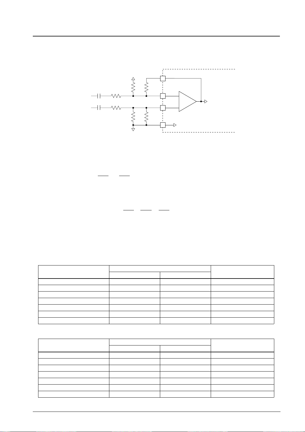
3.3 Input Amp Circuit
3.3.1 Differential Input
The amp at the input stage must have its circuit configured to allow gain to be set correctly. For this reason, it
requires five to six external resistors.
INN
To filter
Amp
–
+
INP
TIP
RING
FB
R5R3
R6R4
R1
R2
VREF
VREF
VREF
Figure 3.3.1 Input amp circuit
The gain in the input amp can be set depending on values R1to R6as shown below. Note that R3and R5may be
replaced by one resistor.
[times] (WhenR1= R2, R 3= R4, R5= R6)
R6
R2
=
R5
R1
GAMP =
To set the FSK and CAS tone signal-detection levels, determine each resistance value with respect to VDD as shown
below.
R6
R2
=
R5
R1
GAMP =VDD
5
=×0.562[times]
VDD is the power supply voltage fed to the VDD pin of the E0C5251. For R3andR4, SeikoEpsonrecommendsusing
a resistance of about 200 kΩfor noise prevention.
Tables 3.3.1 and 3.3.2 show typical resistance values and amp gain for the case where VDD = 5 V and VDD = 3 V,
respectively. Do not use resistors with lower values than those shown in the table below when the MODE1 pin isset
to 1 (FSK detection during power down).
Table 3.3.1 Resistance values and gain (VDD = 5 V)
Parameter Value Condition
Bellcore BT
R1, R21000 kΩ1000 kΩ1%
R3, R4200 kΩ200 kΩ1%
R5, R6562 kΩ562 kΩ1%
Input amp gain 0.562 times (-5 dB) 0.562 times (-5 dB)
FSK/CPM - CD ON level (Typ.) -43.0 dBm -45.2 dBV
FSK/CPM - CD OFF level (Typ.) -45.0 dBm -47.2 dBV
CAS - CD ON level (Typ.) -35.9 dBm -44.1 dBV Tone filter gain = -4 dB
Table 3.3.2 Resistance values and gain (VDD = 3 V)
Parameter Value Condition
Bellcore BT
R1, R21000 kΩ1000 kΩ1%
R3, R4200 kΩ200 kΩ1%
R5, R6338 kΩ338 kΩ1%
Input amp gain 0.3372 times (-9.4 dB) 0.3372 times (-9.4 dB)
FSK/CPM - CD ON level (Typ.) -43.0 dBm -45.2 dBV
FSK/CPM - CD OFF level (Typ.) -45.0 dBm -47.2 dBV
CAS - CD ON level (Typ.) -35.9 dBm -44.1 dBV Tone filter gain = -4 dB
3 FUNCTIONAL DESCRIPTION
14 EPSON E0C5251 TECHNICAL MANUAL
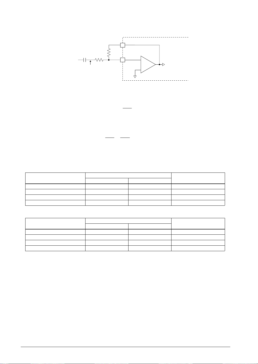
3.3.2 Single End Input
When the amp is used as single end input, two external resistors are required.
CASIN
To filter
Amp
–
+
HYBRID
CASFB
B
R8
R7
Figure 3.3.2 Input amp circuit
The gain in the input amp can be set depending on values R7and R8as shown below.
[times]
R8
R7
GAMP =
To set the FSK and CAS tone signal-detection levels at node B, determine each resistance valuewithrespect toVDD
as shown below.
=
R8
R7
GAMP =VDD
5×0.562 [times]
VDD is the power supply voltage fed to the VDD pin of the E0C5251.
Tables 3.3.3 and 3.3.4 show typical resistance values and amp gain for the case where VDD = 5 V and VDD = 3 V,
respectively.
Table 3.3.3 Resistance values and gain (VDD = 5 V)
Parameter Value Condition
Bellcore BT
R71000 kΩ1000 kΩ1%
R8562 kΩ562 kΩ1%
Input amp gain (Typ.) -5.0 dB -5.0 dB
CAS - CD ON level (Typ.) -35.9 dBm -44.1 dBV Tone filter gain = -4 dB
Table 3.3.4 Resistance values and gain (VDD = 3 V)
Parameter Value Condition
Bellcore BT
R71000 kΩ1000 kΩ1%
R8338 kΩ338 kΩ1%
Input amp gain -9.4 dB -9.4dB
CAS - CD ON level (Typ.) -35.9 dBm -44.1 dBV Tone filter gain = -4 dB
3 FUNCTIONAL DESCRIPTION
E0C5251 TECHNICAL MANUAL EPSON 15
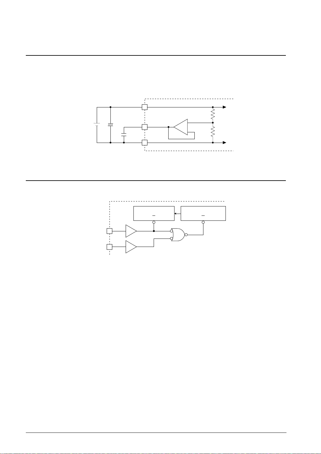
3.4 Ring/Line Reversal Signal Detection
Figure 3.4.1 shows a typical circuit used to detect the Bellcore ring signal andBritishTelecomLineReversalsignal.
When the E0C5251 is in power-down mode, this circuit detects the ring signal or Line Reversal signal. The Line
Reversal or ring signal causes the voltage on the RDIN pin to rise, which drives the Schmitt rigger outputhigh. This
causes the Nch transistor to turn on and the #RDRC pin to change to Low level. Since the RDIN pin is normally at
the VSS level, the #RDRC pin is at the High level. When the ring signal is input or the Line Reversal signal is
generated, the capacitor of the #RDRC pin discharges, causing the #RDRC pin to change state from High to Low.
The #RDET pin operates in the same way, except that in any mode other than power-down mode, the #RDET pin
always responds to input on the RDIN pin.
#IRQ
RDIN
TIP
RING #RDRC VDD
VDD
#DET
#RDET
VDD
270 kΩ
0.2 µF
0.2 µF
0.2 µF
33 kΩ
470 kΩ
Figure 3.4.1 Ring/line reversal signal detection circuit
3.5 FSK Demodulation
The received FSK-modulated signal, after being processed by the band-pass filter, is demodulated by the FSK
demodulation circuit. If the FSK signal is input when the PDWN pin is set to Low level and FSK mode has been
selected by the host CPU, the #DET pin changes to Low level. The received data is read out from the SDO pin by
the host CPU. Also, the #IRQ pin is driven Low each time one byte is received. This demodulationcircuitsupportsa
FSK-modulated signal that conforms to ITU-T V.23 or Bell202.
Table 3.5.1 FSK data characteristics
Parameter Bellcore BT
Mark frequency 1200 Hz ±1% 1300 Hz ±1.5%
Space frequency 2200 Hz ±1% 2100 Hz ±1.5%
Receive signal level Mark: -32 dBm to -12 dBm
Space: -36 dBm to -12 dBm Mark: -40 dBV to -14 dBV
Space: -36 dBV to -8 dBV
Signal distortion ≥25 dB ≥20 dB
Transfer rate 1200 baud ±1% 1200 baud ±1%

3 FUNCTIONAL DESCRIPTION
16 EPSON E0C5251 TECHNICAL MANUAL
3.6 Dual-Tone Detection
Dual tones (Bellcore CPE alert signal (CAS), British Telecom tone alert signal) are detected using two tone filters
and digital identification circuits. If dual tones are received when the PDWN pin is set low and CAS mode has been
selected by the host CPU, the #DET pin and the #IRQ pin changes to Low level.
Table 3.6.1 Dual-tone characteristics
Parameter Bellcore BT (tone alert signal)
(CPE alert signal) Line disconnected Line connected
Low tone frequency 2130 Hz ±0.5% 2130 Hz ±1.1% 2130 Hz ±0.6%
High tone frequency 2750 Hz ±0.5% 2750 Hz ±1.1% 2750 Hz ±0.6%
Receive signal level -32 dBm to -14 dBm/tone,
off-hook -40 dBV to -2 dBV/tone,
on-hook -40 dBV to -8 dBV/tone,
off-hook
Rejection signal level ≤-45 dBm ≤-46 dBV
Receive tone twist 0 to 6 dB 0 to 7 dB 0 to 7 dB
Tone outputtime 75 msec to 85 msec 88 msec to 110 msec 80 msecto 85 msec
Simultaneous voice
reception Yes No Yes
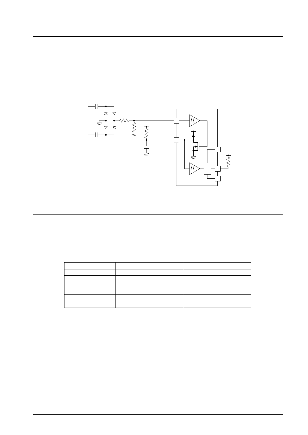
3.7 Off-Hook Detection
Figure 3.7.1 shows an example of an off-hook detection circuit. Set the MODE1 pin to 1 to detect off-hook status.
The example below can detect on-hook/off-hook status even if the device is in the power down mode. The hook
status is detected by comparingthe voltage values between the HOOK and EXTREF pins. When off-hook (HOOK
pin voltage < EXTREF pin voltage) is detected, the #RDET pin outputs 0.
HOOK
TIP
RING
RING
MODE1 = 1
EXTREF #RDET
Amp( )
–
+
Figure 3.7.1 Off-hook detection circuit
Table of contents


