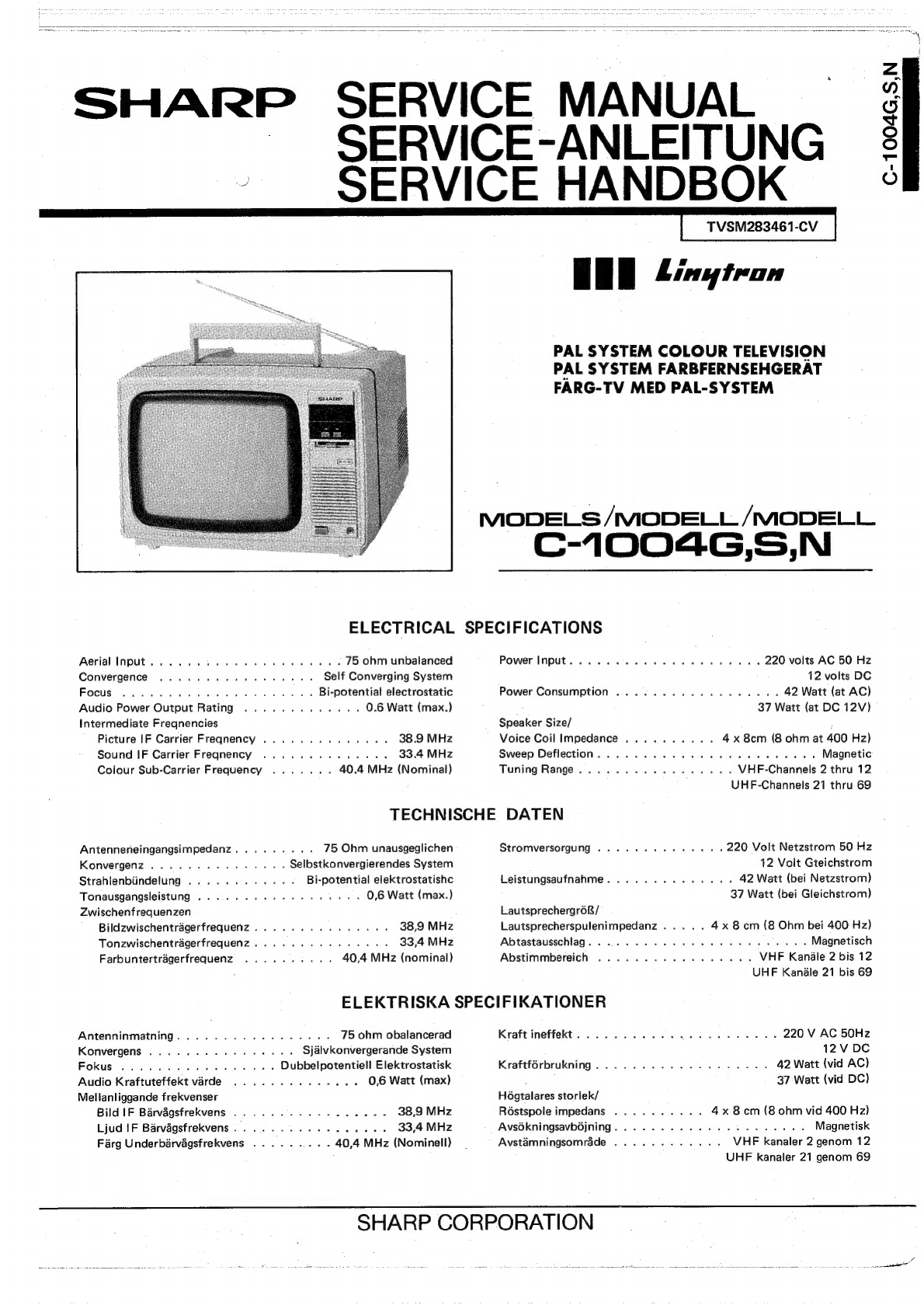
Sharp Linytron C-1004G User manual

SHARP
SERVICE
MANUAL
SERVICE-ANLEITUNG
?
SERVICE
HANDBOK
|
Ef fl
Linyteon
PAL
SYSTEM
COLOUR
TELEVISION
PAL
SYSTEM
FARBFERNSEHGERAT
FARG-TV
MED
PAL-SYSTEM
MODELS
/MODELL.
/MODELL.
C-1004G,S,N
ELECTRICAL
SPECIFICATIONS
Aerial
Input...
2.
ee
ee
ee
75
ohm
unbalanced
Power
[nputic-es
ood.
6
Sek
nes
ae
ae
ah
220
volts
AC
50
Hz
Convergence
........
cee
eee
Self
Converging
System
12
volts
DC
FOGUS:
<<.
sseehclecehun
woety
Bb
ee
ee
ee
Bi-potential
electrostatic
Power
Consumption
..........00
50584
e
ae
42
Watt
(at
AC)
Audio
Power
Output
Rating
..........005
0.6
Watt
(max.)
37
Watt
(at
DC
12V)
Intermediate
Freqnencies
Speaker
Size/
:
Picture
IF
Carrier
Freqnency
..............
38.9
MHz
Voice
Coil
Impedance
..........
4
x
8cm
(8
ohm
at
400
Hz)
Sound
IF
Carrier
Freqnency
............24.
33.4
MHz
Sweep
Deflection...
2...
0...
ee
ee ee
ees
Magnetic
Colour
Sub-Carrier
Frequency
.......
40.4
MHz
(Nominal)
Tuning
Range.
..........
00200
VHF-Channels
2
thru
12
UHF-Channels
21
thru
69
TECHNISCHE
DATEN
Antenneneingangsimpedanz.........
75
Ohm
unausgeglichen
Stromversorgung
..
1...
6
ee ee
ee
220
Volt
Netzstrom
50
Hz
Konvergenz
..
2...
0...
ee
eee
Selbstkonvergierendes
System
42
Volt
Gteichstrom
Strahienbiindelung
..........--
Bi-potential
elektrostatishc
Leistungsaufnahme.
..........06.%
42
Watt
(bei
Netzstrom)
Tonausgangsleistung
..
2...
2
ee
ee
es
0,6
Watt
{max.)
37
Watt
(bei
Gleichstrom)
Zwischenfrequenzen
Lautsprechergr68/
Bildzwischentragerfrequenz
........-.-..200%
38,9
MHz
Lautsprecherspulenimpedanz.....
4
x
8
cm
(8
Ohm
bei
400:Hz)
Tonzwischentragerfrequenz....
2.1...
2
eee
eee
33,4
MHz
Abtastausschlag.
.
2...
ee
ee
es
Magnetisch
Farbuntertragerfrequenz
......:...
40,4
MHz
(nominal)
Abstimmbereich
.......0...-
002004
VHF
Kanile
2
bis
12
UHF
Kandle
21
bis
69
ELEKTRISKA
SPECIFIKATIONER
Antenninmatning.
.......002
2.220
75
ohm
obalancerad
Kraft
ineffekt.........0.0.,
BA
th
Segla
SR
B68,
MS
220
V
AC
50Hz
Konvergens
........020
08005
Sjalvkonvergerande
System
12V
DC
FOKUS:
hse
i
veces
oh
a
eh
Dubbelpotentiell
Elektrostatisk
Kraftférbrukning.
2.2...
ee
ee
ee
eee
42
Watt
(vid
AC)
Audio
Kraftuteffekt
varde
..........-.45
0,6
Watt
(max)
:
37
Watt
(vid
DC)
Mellanliggande
frekvenser
Hégtalares
storlek/
Bild
IF
Barvagsfrekvens
.......-.-.-..000-
38,9
MHz
Réstspole
impedans
..........
4
x
8
cm
(8
ohm
vid
400
Hz)
Ljud
IF
Barvagsfrekvens
..
2...
ee
eee
eee
33,4
MHz
Avs6kningsavbéjning....
2...
.
eee
ee
ee
Magnetisk
Farg
Underbarvagsfrekvens
.........
40,4
MHz
(Nominell)
_
Avstamningsomrade
.......-...-
VHF
kanaler
2
genom
12
UHF
kanaler
21
genom
69
C-1004G,S,N

Page
ELECTRICAL
SPECIFICATIONS
.........0.0..
1
CHASSIS
LAYOUT
DIAGRAM
.............
IMPORTANT
SERVICE
NOTES..........-.05.
3
PRINTED
WIRING
BOARD
ASSEMBLIES......
DESCRIPTION
OF
NEW
CIRCUIT
.............
4
SCHEMATIC
DIAGRAMS
AND
WAVEFORMS...
ADJUSTMENT
1.2.2...
0
cee
eee
ee
eee
eee
7
REPLACEMENT
PARTS
LIST
..............
TROUBLE
SHOOTING
TABLE
............-.---
12
INHALT
Seite
TCHNISCHE
DATEN
.......
20:
ee
eee
ee
eee
i]
CHSISANORDNUNGSPLAN
...........
so
A
WICHTIGE
SERVICE-ANMERKUNGEN
.........
20
LEITERPLATTENEINHEITEN
.............
BESCHREIBUNG
DER
NEUEN
KREISES
........
21
SCHEMATISCHER
SCHALTPLAN
UND
EINSTELLUNGEN...
2...
00...
eee
ee
eee
24
WELLENFORMEN.........
00+.
e
eae
FEHLERSUCHTABELLE
............225
eee
29
ERSATZTEILLISTE...
2...
cc
ee
ee
ee
INNEHALL
Sid
ELEKTRISKA
SPECIFIKATIONER
............
1
FELSOKNINGSCHEMA
..........0
00+
eee
OBSERVERA
VID
SERVICEATGARD
..........
37
CHASSIPLANRITNING
........
000
eeu
eee
BESKRIVNING
AV
NYA
KRETSAR
...........
38
KRETSKORT
MED
KOPPLINGSSCHEMA......
JUSTERINGAR
..
0...
0.
cee
ee
eee
es
41
PRINCIPSCHEMAN
OCH
FREKVENSKURVOR.
.
RESERVDELSBETECKNING
..........000.
WARNING
The
chassis
in
this
receiver
is
partially
hot.
Use
an
isolation
transformer
between
the
line
cord
plug
and
power
receptacle,
when
servicing
this
chassis.
To
prevent
electric
shock,
do
not
remove
cover.
No
user
—
serviceable
parts
inside.
Refer
servicing
to
qualified
service
personnel.
WARNUNG
Das
Chassis
dieses
Empfangsgerites
steht
teilweise
unter
hohen
Spannungen.
Bei
Wartungsarbeiten
an
diesem
Chassis
mu
deshalb
ein
Isolationstransformator
zwischen
dem
Netzkabelstecker
und
der
Steck-
dose
verwendet
werden.
Um
elektrische
Schlage
zu
vermeiden,
darf
das
Abdeckgehduse
nicht
entfernt
werden.
Im
Inneren
des
Gerites
befinden
sich
keine
vom
Benutzer
einstellbaren
Teile.
Wartung
und
Reparaturarbeiten
miissen
qualifiziertem
Service-Personal
tiberlassen
werden.
VARNING
Chassiytan
ar
delvis
het.
Anvand
alltsa
en
isoleringstransformator
mellan
vaxelstr6mskontakten
och
strémingangen
nar
nagot
servicearbete
skall
utféras
pa
chassit.
Ta
inte
bort
chassiomhéljet
fér
fara
av
elektriska
sttar.
Forsék
aldrig
att
sjalv
utfGra
nagra
serviceatgarder
inne
i
apparaten
utan
vand
till
kvalificerad
personal.
Sid

IMPORTANT
SERVICE
NOTES
Maintenance
and
repair
of
this
receiver
should
be
done
by
qualified
service
personnel
only.
SERVICING
OF
HIGH
VOLTAGE
SYSTEM
AND
PICTURE
TUBE
When
servicing
the
high
voltage
system,
remove
static
charge
from
it
by
connecting
a
10k
ohm
Resistor
in
series
with
an
insulated
wire
(such
as
a
test
probe)
between
picture
tube
dag
and
2nd
anode
lead.
(AC
line
cord
should
be
disconnected
from
AC
outlet.)
1.
Picture
tube
in
this
receiver
employs
integral
implosion
protection.
2.
Replace
with tube
of
the
same
type
number
for
continu-
ed
safety.
3.
Do
not
lift
picture
tube
by
the
neck.
4.
Handle
the
picture
tube
only
when
wearing
shatter-proof
goggles
and
after
discharging
the
high
voltage
com-
pletely.
X-RAY
This
receiver
is
designed
so
that
any
X-ray
radiation
is
kept
to
an
absolute
minimum.
Since
certain
malfunctions
or
servicing
may
produce
potentially
hazardous
radiation
with
prolonged
exposure
at
close
range,
the
following
pre-
cautions
should
be
observed:
1.
When
repairing
the
circuit,
be
sure
not
to
increase
the
high
voltage
to
more
than
24.5kV,
(at
beam
470uA)
for
the
set.
.
To
keep
the
set
in
a
normal
operation,
be
sure
to
make
it
function
on
18.0kV
+
2.0kV
(at
beam
470yA)
in
the
case
of
the
set.
The
set
has
been
factory
-
adjusted
to
the
above-mentioned
high
voltage.
’.
If
there
is
a
possibility
that
the
high
voltage
fluctuates
as
a
result
of
the
repairs,
never
forget
to
check
for
such
high
voltage
after
the
work.
.
Do
not
substitute
a
picture
tube
with
unauthorized
types
and/or
brands
which
may
cause
excess
X-ray
radiation.
BEFORE
RETURNING
THE
RECEIVER
Before
returning
the
receiver
to
the
user,
perform
the
following
safety
checks.
1.
Inspect
all
lead
dress
to
make
certain
that
leads
are
not
pinched
or
that
hardware
is
not
lodged
between
the
chassis
and
other
metal
parts
in
the
receiver.
.
Inspect
all
protective
devices
such
as
non-metallic
con-
trol
knobs,
insulating
fishpapers,
cabinet
backs,
adjust-
ment
and
compartment
covers
or
shields,
isolation
resistor-capacity
networks,
mechanical
insulators
etc.
I

DESCRIPTION
OF
NEW
CIRCUIT
DC-DC
Inverter
Circuit
This
model
is
provided
with
a
DC-DC
inverter
circuit
so
that
it
can
be
used
outdoors
operating
on
the
automobile
battery
(12V
DC).
AC
operation
and
DC
operation
are
changed
from
each
other
automatically
by
using
the
AC
or
DC
power
cord
to
connect
it
to
the
set.
,
The
DC-DC
inverter
circuit
ensures
not
only
to
amplify
the
output
voltage
but
also
to
regulate
the
input
voltage
against
its
fluctuation.
Fig.
1
is
a
block
diagram
of
the
DC-DC
inverter
circuit.
The
square-wave
signal
which
has
been
caused
by
the
hori-
zontal
oscillator
circuit
(IC501)
is
first
applied
to
the
integ-
ration
circuit
where
it
is
converted
to
a
sawtooth-wave
signal
to
be
fed
to
the
pulse-width
converter
circuit.
In
the
pulse-width
converter
circuit,
the
sawtooth-wave
signal
is
again
converted
into
a
square-wave
signal
then
entering
the
inverter
drive
circuit
where
it
is
amplified
enough
to
drive
the
inverter
output
circuit.
The
output
voltage
from
the
inverter
output
circuit
is
set
to
+115V
DC,
and
it
is
applied
to
the
error
detection
circuit
where
it
is
compared
with
the
reference
voltage
to
control
the
pulse-width
converter
circuit.
Fig.
2
shows
what
parts
the
inverter
circuit
is
composed
of
and
Fig.
3
reveals
the
waveforms
of
the
voltages
which
are
available
at
the
points
@
to
®
in
Fig.
2.
Coming
from
the
horizontal
oscillator
circuit,
the
square-
wave
voltage
appears
at
the
point
@)
and
is
integrated
by
R779
and
C775
so
that
it
is
converted
into
a
triangular-
wave
voltage
as
shown
in
Fig.
3-(B).
The
triangular-wave
voltage
is
applied
to
the
base
of
Q2:
this
transistor
Q2
is
biased
to
turn
on
only
with
the
voltage
which
is
lower
than
the
level
indicated
by
the
chained
line
in
Fig.
3-(B).
Now
that
the
triangular-wave
voltage
shown
-
by
the
solid
line
in
Fig.
3-(C)
is
applied
to
the
base
of
Q2,
the
transistor
Q2
turns
on
only
when
it
is
given
the
voltage
Integra-
tion
circuit
indicated
by
the
shaded
area
in
Fig.
3-(B):
as
the
result,
at
the
point
©
in
Fig.
2
there
appears
the
voltage
having
the
waveform
indicated
by
the
solid
line
in
Fig.
3-(C).
Then
the
voltage
is
sent
to
Q3
where
its
waveform
is
in-
verted
to
be
the
one
shown
in
Fig.
3-(D).
The
transistor
Q3
is
to
activate
the
drive
transformer
T770.
Actually
when
Q3
turns
off,
T771
is
allowed
to
turn
on
to
get
the
output
transistor
Q770
in
operation;
the
voltage
caused
at
the
point
©
in
Fig.
2
(at
the
base
of
Q770)
has
the
waveform
as
shown
in
Fig.
3-(E).
The
voltage
at
the
collector
of
Q770
has
the
waveform
as
shown
in
Fig.
3-(F)
while
the
current
there
of
has
the
waveform
as
shown
in
Fig.
3-(G).
The
output
voltage
from
the
inverter
transformer
is
applied
to
D775
where
it
is
rectified
as
long
as
Q770
is
turned
off:
that
is
to
say,
when
Q770
is
turned
on,
the
magnetic
energy
-
at
T771
increases
so
that
the
output
voltage
from
D775
also
increases.
The
rectified
output
voltage
is
then
sent
to
the
succeeding
load
circuit.
However,
a
part
of
it
is
fed
back
to
Q1
and
then
to
Q2
via
ZD1
to
control
biasing
of
Q2.
Now
suppose
that
there
is
a
rise
of
the
output
voltage
of
the
transformer
due
to
some
reasons
(e.g.
due
to
an
increase
of
input
DC
voltage
or
an
alleviation
of
the
output
load).
Then
the
current
at
the
base
of
Q1
increases
with
its
collector’s
current
also
increasing.
Therefore
the
voltage
at
the
base
of
Q2
decreases
and
this
means
that
the
turn-on
time
of
Q2
becomes
longer
than
before:
the
output
wave-
form
then
caused
refers
to
that
indicated
by
the
brokin
line
in
Fig.
3B).
The
output
waveforms
available
thereafter
are
those
indicated
by
the
broken
lines
in
Fig.
3-(C),
-(D),
4E),
-(F)
and
(G):
this
fact
is
to
shorten
the
turn-
on
time
of
Q770
so
as
to
decrease
the
magnetic
energy
charged
in
T771.
As
the
result,
the
output
voltage
from
T771
which
has
been
higher
than
specified
is
now
decreased
to
its
normal
level.
Pulse
width
Inverter
Inverter
converter
drive
output
circuit
circuit
circuit
Error
detector
circuit
'
OUT
DC
115V

___g
1C501
1XO065CE
+12V
DC
IN-PUT
Z0103CE
1771
rc
:
1770
1X0248CE
0000000
L771
+
C776
Voltage
waveform
at
point
@
ov
Voltage
waveform
at
point
®
2
turn-on
level
Figure
2.
+115V
DC
OUT-PUT
Voltage
waveform
at
point
©
Voltage
waveform
at
point
©
Voltage
‘waveform
at
point®
”°
Voltage
waveform
at
point
©
Current
waveform
at
2
collector
of
Q770
eee
Serene
Lage
ro
eats
Be
Figure
3.
C780
|
|
|
|
|
|
|
|
|
|
|
|
|
|
epee
|

The
DC-DC
inverter
circuit
has
two
built-in
functions
for
its
safer
operation,
which
are
described
below.
(i)
Overload
preventive
function
After
passing
through
F770,
the
supply
voltage
(12V
DC)
is
separated
into
three
currents
i,,
i,
and
i;.
the
current
i
is
applied
to
the
output
transistor
Q770
to
make
it
ready
to
be
in
operation.
The
current
i,
is
sent
via
R651
to
pin
@)
of
IC5O1
so
that
1501
is
in
operation
the
output
of
which
appears
at
the
point
@):
at
the
same
time,
the
transistor
Q2
turns
on
to
cause
an
output
signal
at
its
collector.
Further
the
current
i;
is
applied
via
C774
to
the
primary
side
of
T770
the
output
of
which
is
instantly
impressed
onto
the
base
of
Q770.
With
Q770
turned
on,
there
is
an
instant
output
of
DC
voltage
between
pins
@)
and
(5)
of
T771
which
is
applied
to
D775
for
the
rectification.
At
the
same
time,
there
is
also
an
instant
output
of
DC
voltage
bet-
ween
pins
and
@)
of
T771
and
is
fed
to
D770
for
the
rectification.
The
output
current
from
D770
is
separated
into
two
currents
i,
and
is:
the
former
is
sent
via
D773
and
R651
to
IC5O1,
and
the
latter
to
Q3.
Usually
the
rectification
DC
output
from
D770
is
about
18V,
and
since
it
is
higher
than
the
power
supply
voltage
(about
12
V),
the
voltage
at
the
cathode
of
D772
becomes
higher
than
its
anode
so
that
this
diode
D772
turns
off.
However,
if
there
occurs
an
overload
at
the
output
circuit
(due
to
its
shortcircuit,
for
example),
no
voltage
is
generated
between
pins
and
(6)
of
T771
so
that
the
inverter
circuit
gets
in
a
stop
automatically:
at
the
time,
however,
the
oscillator
circuit
[501
is
still
in
operation
since
it
is
given
i,
from
D772.
When
the
inverter
circuit
is
stopped
in
this
way,
first
turn
off
the
power
switch
to
discharge
C774,
and
about
10
second
thereafter,
turn
on
the
power
switch
again
to
cause
the
inverter
circuit
to
restart.
(ii)
Input
reverse-connection
preventive
function
The
diode
D771
is
connected
in
parallel
to
the
power
supply
circuit
(12V
DC):
actually,
the
cathode
and
anode
of
the
former
are
connected
respectively
to
the
plus
(+)
terminal
and
minus
(—)
terminal
of
the
latter.
With
this
design,
the
diode
is
usually
kept
turned
off
as
far
as
the
input
connection
of
the
car
battery
cord
is
made
in
a
proper
way.
But
if
the
input
connection
with
reverse
polarity
is
made
as
shown
in
Fig.
4,
D771
turns
on
and
F770
is
shorted
to
be
blown
out.
With
F770
blown
out,
the
inverter
circuit
gets
in
a
stop
not
suffering
any
further
trouble.
Figure
5
shows
the
other
way
of
connection
in
which
a
diode
is
connected
in
series
to
the
power
supply
circuit
(12V
DC).
With
this
design,
the
diode
turns
off,
with
the
fuse
being
not
blown
out,
if
the
reverse
connection
of
the
car
battery
cord
is
performed.
With
the
diode
turned
off,
the
inverter
circuit
stops
its
operation
thus
suffering
no
fur-
ther
trouble.
__
However,
this
design
has
such
a
drawback
that
the
diode
is
kept
turned
on
as
long
as
the
set
is
normally
operating:
this
refers
to
the
power
consumption
of
about
4.5W
needed
for
the
diode
to
operate.
To
vaoid
this
unnecessary
power
consumption,
this
set
employs
the
protective
circuit
shown
in
Fig.
4
instead
of
that
shown
in
Fig.
5.
Inverter
circuit
Figure
4.
Inverter
circuit
Figure
5.

ADJUSTMENT
COLOUR
PURITY
ADJUSTMENT
For
best
results,
it
is
recommended
that
the
purity
adjust-
ment
be
made
in
final
receiver
location.
If
the
receiver
will
be
moved,
perform
this
adjustment
with
it
facing
east.
The
receiver
must
have
been
operating
15
minutes
prior
to
this
procedure
and
the
faceplate
of
the
CRT
must
be
at
room
temperature.
The
receiver
is
equipped
with
an
automatic
degaussing
circuit.
However,
if
the
CRT
shadow
mask
has
become
excessively
magnetized,
it
may
be
necessary
to
degauss
it
with
manual
coil.
Do
not
switch
the
coil
OFF
while
the
raster
shows
any
effect
from
the
coil.
The
following
procedure
is
recommended
while
using
a
Dot
Generator.
1.
Check
for
correct
location
of
all
neck
components.
(See
Figure
6.)
2.
Rough-in
the
static
convergence
at
the
center
of
the
CRT,
as
explained
in
the
static
convergence
procedure.
3.
Rotate
the
picture
control
to
centre
of
its
rotation
range
and
rotate
Brightness
control
to
maximum
CW
position.
4.
To
obtain
a
blank
raster,
connect
a
short
clip
lead
be-
tween
pin
2
of
IC801
and
earth.
Then,
rotate
screen
control
CW
until
normal
raster
is
obtained.
5.
Rotate
the
Red
Bias
and
Blue
Bias
controls
to
maximum
CCW
position
Rotate
the
Green
bias
control
sufficiently
in
a
CW
direction
to
produce
a
green
raster.
6.
Loosen
the
deflection
yoke
tilt
adjustment
wedges
(three),
loosen
the
deflection
yoke
clamp
screw
and
push
the
deflection
yoke
as
close
as
possible
to
the
CRT
screen.
7,
Begin
the
following
adjustment
with
the
tabs
on
the
round
purity
magnet
rings
set
together,
initially
move
the
tabs
on
the
round
purity
magnet
rings
to
the
side
of
the
CRT
neck.
Then,
slowly
separate
the
two
tabs
while
_
at
the
same
time
rotating
them
to
adjust
for
a
uniform
green
vertical
band
at
the
centre
of
the
CRT
screen.
8.
Carefully
slide
the
deflection
yoke
backward
to
achieve
green
purity
(uniform
green
screen).
NOTE:
Center
purity
was
obtained
by
adjusting
the
tabs
on
the
round
purity
magnet
rings,
outer
edge
purity
was
obtained
by
sliding
the
deflection
yoke
forward.
Tighten
the
deflection
yoke
clamp
screw.
9,
Check
for
red
and
blue
field
purity
by
reducing
the
output
of
the
Green
Bias
control
and
alternately
in-
creasing
output
of
Red
and
Blue
Bias
controls
and
touch
up
adjustments,
if
required.
10.
Disconnect
between
pin
@2
of
IC801
and
earth,
if
connect
in
connect
in
step
4.
11.
Perform
BLACK
AND
WHITE
TRACKING
procedure.
STATIC
(CENTER)
CONVERGENCE
ADJUSTMENT
1.
Switch
the
Receiver
ON
and
allow
it
to
warm
up
for
15
minutes.
2.
Connect
the
output
of
a
Crosshatch
Generator
to
the
Receiver
and,
concentrating
on
the
centre
of
the
CRT
screen,
proceed
as
follows:
a.
Locate
the
pair
of
4
pole
magnet
rings.
Rotate
indi-
vidual
rings
(change
spacing
between
tabs)
to
con-
verge
the
vertical
red
and
blue
lines.
Rotate
the
pair
of
rings
(maintaining
spacing
between
tabs)
to
converge
the
horizontal
red
and
blue
lines.
b.
After
completing
red
and
blue
centre
convergence,
locate
the
pair
of
6
pole
magnet
rings.
Rotate
indi-
vidual
rings
(change
spacing
between
tabs)
to
con-
verge
the
vertical
red
and
blue
(magenta)
and
green
lines.
Rotate
the
pair
of
rings
(maintaining
spacing
between
tabs)
to
converge
the
horizontal
red
and
blue
(magenta)
and
green
lines.
DEFLECTION
YOKE
PURITY
MAGNETS
CLAMP
SCREW
6
POLE
CONV.
MAGNETS
L,
POLE
CONV,
MAGNETS
L
DEFLECTION
YOKE
TILT
ADJUSTMENT
WEDGE
|
DEFLECTION
YOKE
TAPE
Figure
6.
Picture
Tube
Neck
Components
Location

DYNAMIC
CONVERGENCE
ADJUSTMENT
Dynamic
convergence
(convergence
of
the
three
colour
fields
at
the
edges
of
the
CRT
screen)
is
accomplished
by
proper
insertion
and
positioning
of
three
rubber
wedges
between
the
edge
of
the
deflection
yoke
and
the
funnel
of
the
CRT.
This
is
accomplished
in
the
following
manner.
1.
Switch
receiver
ON
and
allow
it
to
warm
up
for
15
minutes.
2.
Apply
crosshatch
pattern
from
Dot/Bar
Generator
to
receiver.
Observe
spacing
between
lines
around
edges
of
CRT
screen.
3.
Tilt
the
deflection
yoke
up
and
down,
and
insert
tilt
adjustment
wedges
@)
and
@)
between
the
deflection
yoke
and
the
CRT
until
the
mis-convergence
illustrated
in
Fig.
7
@
has
been
corrected.
4.
Tilt
the
deflection
yoke
right
and
left,
and
insert
tilt
adjustment
wedge
(3)
between
the
deflection
yoke
and
the
CRT
until
the
mis-convergence
illustrated
in
Fig.
7
®
has
been
corrected.
5.
Alternately
change
spacing
between,
and
depth
of
in-
sertion
of, the
three
wedges
until
proper
dynamic
con-
vergence
is
obtained.
6.
Use
a
strong
adhesive
tape
to
firmly
secure
each
of
the
three
rubber
wedges
to
the
funnel
of
the
CRT.
7.
Check
purity
and
readjust,
if
necessary.
DEFLECTION
YOKE
REAR
VIEW
Figure
7.
Dynamic
Convergence
Adjustment

(1)
Receive
broadcast
signal
through
extenal
antenna.
TP601
«
tp6e02
«
©
Figure
8.
(1)
Short
TP601
and
TP602.
(2)
Adjust
R607
to
have
almost
proper
horizontal
sync.
(3)
Remove
the
shorting
of
TP601
and
TP602.
|
(1)
Receive
broadcast
signal
through
external
antenna.
LLL.
LLL
SL
LLL
LLL
LLL
Figure
9.
(1)
Fig.
9
(A):
If
the
black
horizontal
line
moves
down
slowly,
turn
V-hold
knob
counterclockwise
to
have
a
proper
sync.
Fig.
9
(B):
If
several
horizontal
lines
appear
at
random,
turn
V-hold
knob
clockwise
to
have
a
proper
sync.
(1)
Connect
pattern
generator
(PM5508)
to
the
unit.
(2)
Set
antenna
input
to
about
70
dB.
(3)
Set
the
pattern
to
“GRAY
SCALE”.
Contrast:
MAX
Brightness:
Set
it
so
that
the
black/
gray
scale
becomes
easy
to
see.
*Tuner
AGC:
Approx.
4V
Figure
10.
(1)
Turning
RF-AGC
(R209)
clockwise
will
produce
noise
in
picture,
(2)
Turning
RF-AGC
(R209)
counterclockwise
will
remove
such
noise;
but
the
picture,
then,
moves
a
little
to
right
and
its
brightness
somewhat
lessens.
Then,
for
proper
adjustment:
Turn
RF-AGC
fully
clockwise
to
produce
noise,
turn
it
back
gently
to
remove
the
noise
and
stop
just
at
a
point
where
no
phenomenon
such
as
(2)
arises.

No.
Where
to
adjust
Setting
Adjustme
nt
4
Chroma
(I)
(1)
Connect
pattern
generator
(1)
Set
the
pattern
to
“MATRIX”.
(PM5508)
to
the
unit,
and
(2)
Adjust
T801
to
obtain
uniform
set
antenna
input
to
about
brightness
—
the
same
-
for
every
70
dB
scanning
line.
(2)
Contrast:
MAX
(3)
Set
the
pattern
to
“DELAY”.
Brightness:
MIN
(4)
Adjust
R804
to
obtain
uniform
Color:
about
1/2
brightness
—
the
same
for
every
scanning
line.
(5)
Set
the
pattern
to
“PHASE”
Adjust
T802
to
have
—
the
same
color
shading
in
both
upper
and
lower
parts
of
picture.
Figure
11.
5
Picture
tube
(1)
Connect
pattern
generator
(1)
Short
TP401
and
TP402.
(PM5508)
to
the
unit.
(2)
Set
the
pattern
to
“GRAY
SCALE”
(3)
Contrast:
MAX
Brightness:
MAX
cut-off
adjust
9
1404
ce
‘
[_]icso1
TP403
TP401
e
e
|
1C201
TP402
TUNER
FBT
Figure
12.
R863
R857
(B-Drive)
(G-Drive)
R853
(R-Bias)
R854
(G-Bias)
R865
(B-Bias)
Figure
13.
(2)
Short
TP403
and
TP404.
(3)
Set
G-drive
control
(R357)
and
B-drive
control
(R863)
to
abour
“1/2”.
(4)
Turn
R-bias
control
(R853)
G-bias
control
R859)
and
B-bias
control
(R865)
counterclockwise
to
their
maximum
extent.
(5)
Turn
screen
control
(R626),
from
its
minimum
position,
slowly
clockwise
to
make
a
slight
horizontal
line
come
into
existence,
and
stop
it.
(6)
Adjust
the
R853,
R859
and
R865
separately
to
make
that
horizontal
line
equally
colored
for
every
color.
(R,
G
and
B).
However,
if
the
color
appearing
at
first
is,
for
instance,
red
never
touch
the
R853
but
only
the
R859
and
R865
—
the
same
holds
true
for
the
colors
green
and
blue
when
they
appear
at
first.
(7)
Turn
the
screen
control
V.R
clockwise
to
vanish
the
horizontal
line,
and
stop.

Where
to
adjust
White
balance
Beam
current
setting
(1)
Connect
voltmeter
B®
to
TP603
and
©
to
TP604.
(2)
Set
the
pattern
to
“GRAY
SCALE”.
(3)
Contrast:
MAX
Brightness:
MAX
Adjustment
(1)
Remove
the
shorting
of
TP401
and
TP402,
and
of
TP403
and
TP404.
(2)
Adjust
G-drive
control
(R857)
and
B-drive
control
(R863)
to
have
colour
temperature
6500°K.
(3)
Adjust
R406
to
make
the
voltmeter
0.415V,
Sub-sound
Sub-S
(A)
(1)
Sound
V.R
(R1010):
MAX
(2)
Connect
pattern
generator
(PM5508)
to
the
unit.
(3)
Set
sound
carrier
to
100%
modulation.
(4)
Connect
oscilloscope
to
U3.
Adjust
R302
to
make
the
output
2.5Vp-p.
©)
R302
©
TP301
Figure
14,
Sub-S
(B)
(5)
After
above
adjustment
oscilloscope
to
TP301.
=
Adjust
R1009
to
make
the
output
550mVp-p.
11
|
1¢1001
Figure
15.

TROUBLE
SHOOTING
TABLE
CHANNEL
CAN'T
BE
CHANGED
BY
CHANNEL
SWITCH.
When
channel
up
(down)
switch
is
turned
on,
channel
does
not
change.
ier
Check
?
Does
channel
indicator
change?
}
No
|
1C1001
Check
the
voltage
of
1C1001
Pin
(6
(
(9).
[poe
ae
Check
R1019,
C1008
R1019,c1008_—s!
(R1020,
C1009)
|
(F1020,
c1one)
|
apiece
ated
|
Check
swioo1
|
|
(sw1002)
Le
12

Check
the
voltage
of
the
tuner
Bu,
BH,
BL,
+B.
(Approx:
OV
or
12V)
Check
the
voltage
of
Vr
(Change
from
OV
to
30V)
Check
the
voltage
of
1C203.
(Approx:
32V)
Check
!1C203,
R221
Abnromal
Check
band
selector
switch
Abnormal
ro---e
|
Check
1017
|
Oo
en
ae
Check
the
tuner.
|
J
r
{
Check
Q202
and
|
its
adjacent
circuit
Normal
=
|
Check
1C202
|
Lee
ee
st

NO
PICTURE,
SOUND
IS
NOISE
Contrast,
Brightness,
Sound
volume
recheck
and
Abnormai
1C201
bias
check.
Normal
0201
bie
check
Tuner
bias
check
+B
supply
abnormal
AGC
bias
abnormal
a)
th
weay
=
[Sn
em
pe
ne
ne
Ty
pes
Mag
Check 1C202
4
|
AGC
circuit
and
adjacent
I
parts
check
|
ae
cc
re
cee
el
TV
section:
Sound
is
no
noise
R305,
R304
and
7301,
1C301.
ee
—_
Vso
eer
ek
ee
aed
I
|
Q201
and
its
adjacent
parts
check,

UNLOCKED
COLOUR
(NO
COLOUR
SYNCHRONISATION)
Check
1C801
and
bias
control
circuit
X801,
C414, C415,
R419
C410,
C411,
C412
and
NO
COLOUR
Colour
volume
max.
No
colour
Connect
pin
2
and
pin
@
of
IC801
No
colour
rc
——
—
—
—
|
Check
1C801
Pin
29
and
|
|
its
adjacent
parts.
L
1C801

Is
some
colour
produced
in
B/‘
broadcast
reception?
|
Readjust
the
Is
the
white
balance
1C801,
R812,
R813
I
white
balance
properly
adjusted?
and
R814
es
ees
te
as
—4
The
picture
is
coloured
The
picture
is
coloured
The
picture
is
coloured
red
or
cyan
green
or
magenta
blue
or
yellow
ene
ens
a
|
[OFF
Fea
mee
wd
Q851
and
its
adjacent
|
Q852
and
its
Q853
and
its
parts
|
adjacent
parts
adjacent
parts
NO
SYNCHRONISATION
I
|
I
ee
SS
eee
TP601
and
TP602
are
short
circuit,
Normal
Free
run
freq
readjustment
(R504,
R607)
Abnromal
Vertical
Horizontal
ace
ae
|
[tetas
tht
eye
al
|
803,
c504
€611,
C612,
ceos_!
|
|
|
R502,
R623
|
C607,
R6OS
and
and
R503
}
R604

c-
|
R501
and
R509
{
Blown
out
|
Replace
the
fuse
F701
check
Abnormal
bie
eee
R701
and
D702
Abnormal
D704,
D604
check
Normal
[Pose
ee
G7
eel
|
R615,
R611
and
QO601
1C701
Pin
(1)
voltage
check
(Approx
:
280V)
+B1
voltage
check
(Approx
:
115V)
CRT
connector
K1
~
K5
bias
check
Normal
The
fuse
is
again
blown
out
1C701
check
—
[oe
ee
eh
|
C706
and

NO
VERTICAL
SCAN
C503
and
C504
.
os
~
.
re
eT
|
Normal
L
C627,
C517
and
R623
1C502
bias
Dot
Pre
eee
=
3
C509,
R648
and
D502
C508
and
R507
Se
ee
Hs

|
L
roa
T771—f
—-———-]
NO
DC
OPERATE
Q773
collector
voltage
check
(Approx
:
12V)
Check
1770,
C774
D770,
C772
19
Replace
the
fuse
Again
blown
out
D771,C770andQ770_—
[|
roo
1C770

WICHTIGE
SERVICE-HINWEISE
Wartungs-
und
Reparaturarbeiten
an
diesem
Empfanger
sollten
ausschlieflich
von
qualifizierten
Kundendienst-
technikern
ausgefiihrt
werden.
WARTUNG
DES
HOCHSPANNUNGSSYSTEMS
UND
DER
BILDROHRE
Bei
Wartung
des
Hochspannungssystems
leiten
Sie
dessen
Statische
Aufladung
durch
Zwischenschalten
eines
10-
kiloohm-Widerstandes
mit
Hilfe
eines
isolierten
Drahtes
(wie
z.B.
einer
Priifsonde)
zwischen
die
leitende
Graphit-
schicht
der
Bildréhre
und
die
2.
Anodenleitung
ab.
(Der
Netzkabelstecker
solte
dabei
aus
der
Netzsteckdose
gezogen
werden.)
1.
Fiir
die
Bildréhre
in
diesem
Empfanger
wird
ein
inte-
grierter
Implosionsschutz
verwendet.
2.
Ersetzen
Sie
die
Bildréhre
durch
eine
Réhre
mit
der-
selben
Typennummer,
um
eine
dauernde
Sicherbeit
zu
gewahrleisten.
3.
Heben
Sie
die
Bildréhre
nicht
am
Hals
hoch.
4.
Fassen
Sie
die
Bildréhre
nur
dann
an,
wenn
Sie
eine
splitterfreie
Schutzbrille
tragen
und
nachdem
Sie
die
Hochspannung
vollkommen
ableiteten.
RONTGENSTRAHLUNG
Dieser
Empfanger
wurde
so
gebaut,
daf§
Réntgenstrahlung
auf
einem
absoluten
Minimum
gehalten
wird.
Da
durch
bestimmte
Funktionsst6rungen
und
Wartungsarbeiten
beim
langeren
Ausgesetztsein
in
unmittelbarer
Nahe
eine
eventuell
.
gefahrliche
Strahlung
verursacht
werden
kann,
sollten
die
folgenden
Vorsichtmafregeln
beachtet
werden:
1.
Beim
Reparieren
der
Schaltung
darauf
achten,
die
Stromstirke
fiir
das
Gerit
auf
nicht
mehr
als
24,5kV
(Strahlstrom
=
470uA)
zu
erhohen.
2.
Um
das
Gert
in
normalen
Betriebszustand
zu
halten,
darauf
achten,
die
Gerat
iiber
18,0kV
+
2,0kV
(Strahl-
strom
=
470uA)
zu
betreiben.
Das
Gerit
wurde
im
Werk
auf
die
obenerwahnte
Hochspannung
eingestellt.
’.
Falls
die
Méglichkeit
besteht,
da
die
Hochspannung
infolge
von
Reparaturarbeiten
schwankt,
niemals
vergessen,
nach
Beendigung
der
Arbeiten
auf
eine
derartige
Hochspannung
zu
iiberpriifen.
3.
Die
Bild6hre
darf
nicht
gegen
andere
Typen
oder
Bild-
réhren
anderer
Firmen
ausgetauscht
werden,
da
diese
tibermafig
hohe
Réntgenstrahlung
verursachen
kénnten.
VOR
RUCKGABE
DES
EMPFANGERS
Bevor
Die
den
Empfanger
an
den
Kunden
zuriickgeben,
sollten
Sie
die
folgenden
Sicherheitsiiberpriifungen
vor-
nehmen.
;
1.
Uberpriifen
‘Sie
simtliche
Leitungen,
um
sich
zu
ver-
gewissern,
dafi
diese
nicht
eingeklemmt
sind,
oder
daf
sich
keine
Kleinteile
zwischen
dem
Chassis
und
anderen
Metallteilen
im
Empfanger
befinden.
2.
Uberpriifen
Sie
sdmtliche
Schutzvorrichtungen,
wie
z.B.
die
nichtmetallischen
Reglerknépfe,
Isolierpapiere,
Gehauseriickseiten,
Einstell-
und
Zwischenraumab-
deckungen
oder
Abschirmungen,
Isolierwiderstands-
Kapazitatsnetzwerke,
mechnische
Isolatoren
usw.
20
This manual suits for next models
2
Table of contents
Languages:
Other Sharp TV manuals

Sharp
Sharp LD-26SH3U User manual

Sharp
Sharp 70GS-66E User manual

Sharp
Sharp SV-2189N User manual

Sharp
Sharp 28LF-96EC User manual

Sharp
Sharp 21L-FG1RU User manual

Sharp
Sharp CX68LF5 User manual

Sharp
Sharp SX68JS10 User manual

Sharp
Sharp LC-C4254U - 42" LCD TV User manual

Sharp
Sharp AQUOS LC-22SB24U User manual

Sharp
Sharp 14T1-U User manual

Sharp
Sharp 32SF56B User manual

Sharp
Sharp 32R-S480 User manual

Sharp
Sharp LC-46LE810E User manual

Sharp
Sharp 66FW-54H User manual

Sharp
Sharp 29H-FD1S User manual

Sharp
Sharp LC-40FI5122K User manual

Sharp
Sharp LC52LE600E User manual

Sharp
Sharp 21LF-90RU User manual

Sharp
Sharp 27U-S610 User manual

Sharp
Sharp 8C221 User manual