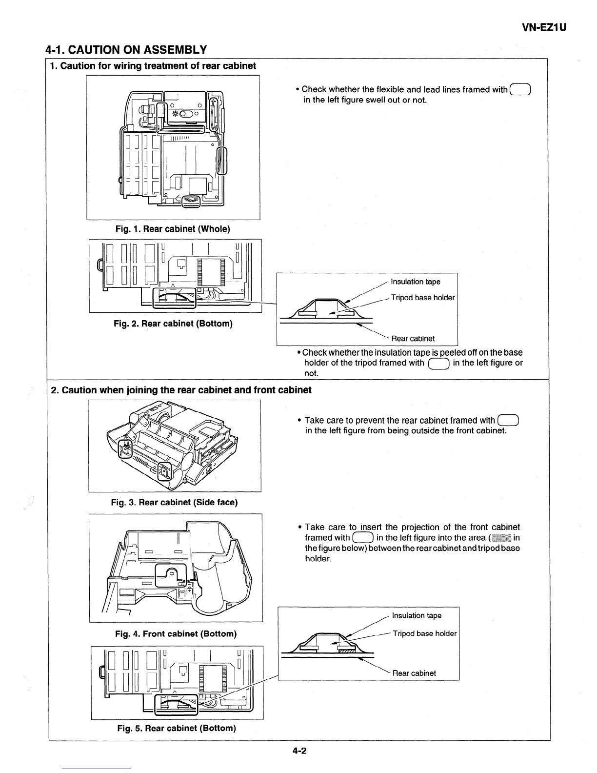
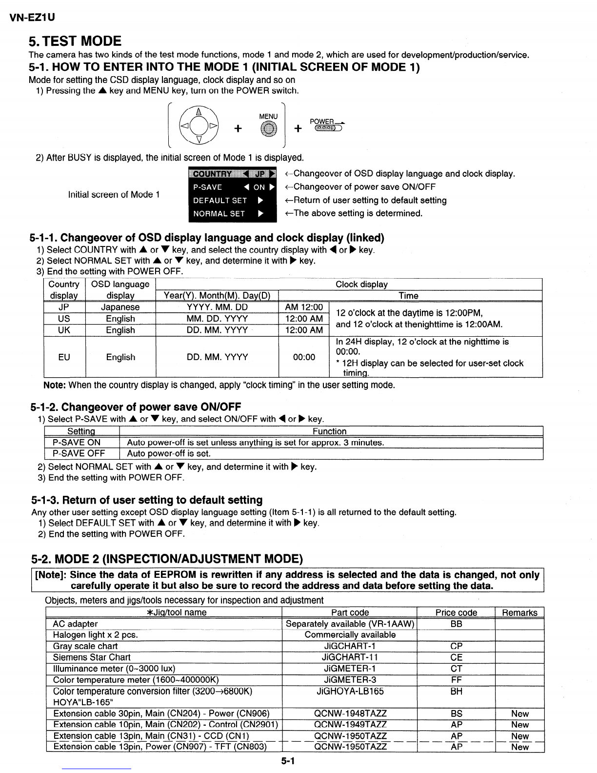
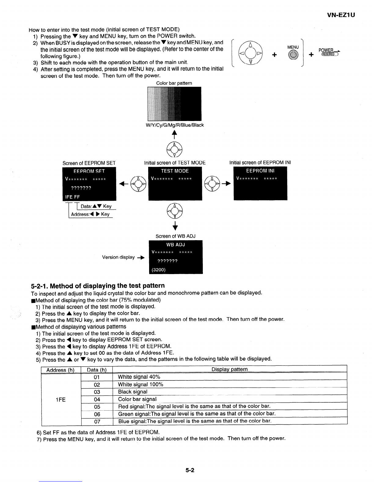
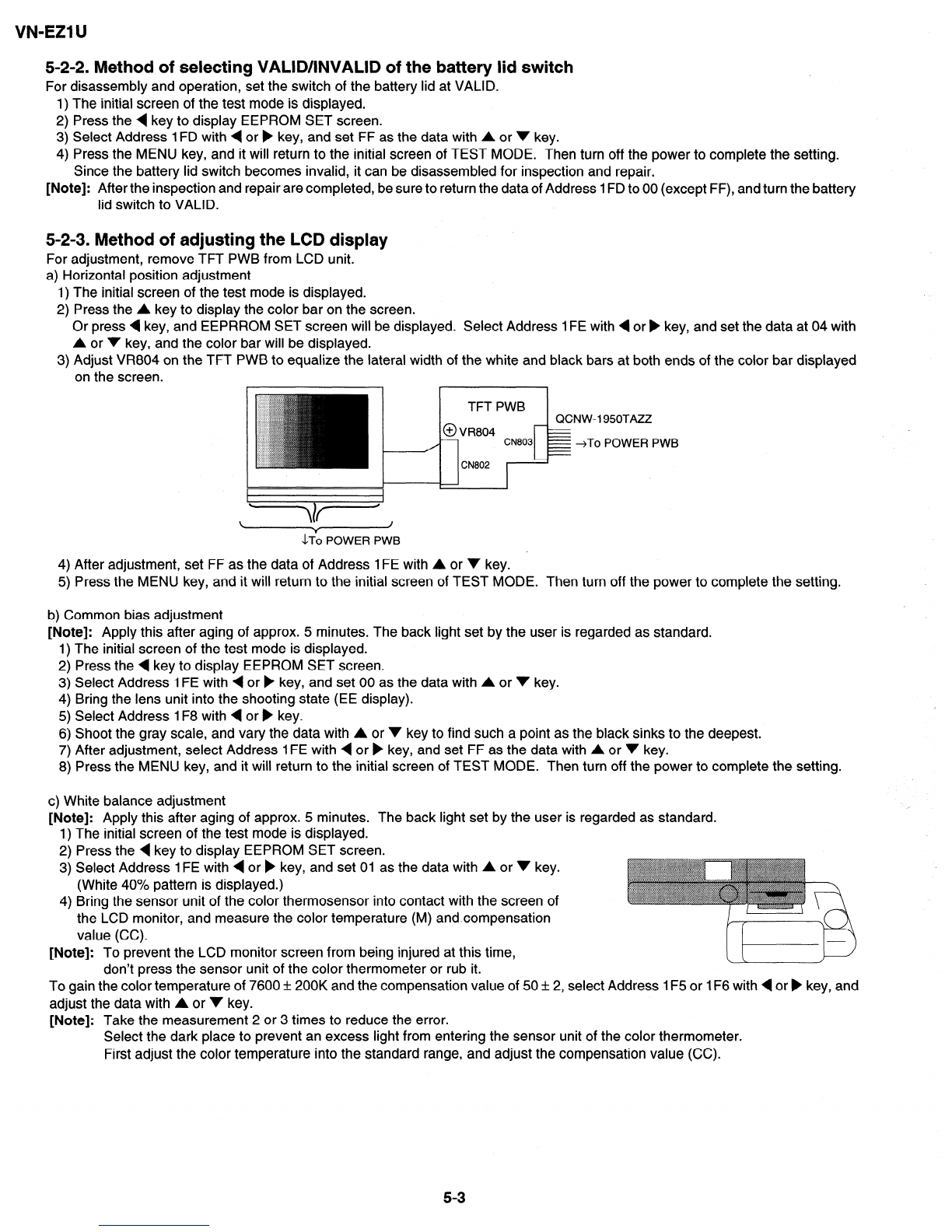
Sharp VN-EZ1U User manual

SHARI= SERVICE MANUAL
S6919VN-EZI U/
MPEG-4 DIGITAL RECORDER
VN-EZI U
In the interests of user-safety (Required by safety regula-
tions in some countries) the set should be restored to its
original condition and only parts identical to those specified
be used. 1
CONTENTS
1.
2.
3.
4.
5.
6.
7.
9.
Page
IMPORTANT SERVICE NOTES ...................................................................................................... l-l
SPECIFICATIONS ........................................................................................................................... 2-l
PART NAMES .................................................................................................................................. 3-l
DISASSEMBLY OF THE SET ......................................................................................................... 4-l
TEST MODE .................................................................................................................................... 5-l
BLOCK DIAGRAM ........................................................................................................................... 6-l
OSCILLATOR, DIVIDING AND MULTIPLY MAP/8. POWER CONTROL FLOW ........................... 7-l
TROUBLESHOOTHING .................................................................................................................. 9-I
.
1O.IC FUNCTION LIST ....................................................................................................................... 10-l
11.SEMICONDUCTOR LEAD IDENTIFICATION ............................................................................... 1l-l
12.WIRING DIAGRAM ........................................................................................................................ 12-I
13.SCHEMATlC DIAGRAMS ............................................................................................................. 13-l
14.PRINTED WIRING BOARD ASSEMBLIES ................................................................................... 14-I
15.REPLACEMENT PARTS LIST ....................................................................................................... 15-1
16,PACKING OF THE SET ................................................................................................................. 16-I
SHARP CORPORATlON This document has been published to be used for
after sales service only.
The contents are subject to change without notice.

VN-EZl U
1. IMPORTANT SERVICE NOTES
BEFORE RETURNING THE VIDEO CAMERA
RECORDER
Before returning the video camera recorder to the user,
perform the following safety checks.
1. Inspect all lead dress to make certain that leads are
not pinched or that hardware is not lodged between
the chassis and other metal parts in the video camera
recorder.
2. Inspect all protective devices such as non-metallic
control knobs, insulating materials, cabinet backs,
adjustment and compartment covers or shields, isola-
tion resistor/capacitor networks, mechanical insula-
tors etc.
connections, metal cabinet, screw heads, knobs and
control shafts, etc.) ,and measure the AC voltage drop
across the resistor. Reverse the AC plug (a non
polarized adaptor plug must be used but only for the
purpose of completing these checks) on the set and
repeat the AC voltage measurements for each ex-
posed metallic part. Any reading of 0.45V rms (this
corresponds to 0.3mA rms AC.) or more is excessive
and indicates a potential shock hazard which must be
corrected before returning the video camera recorder
to the user.
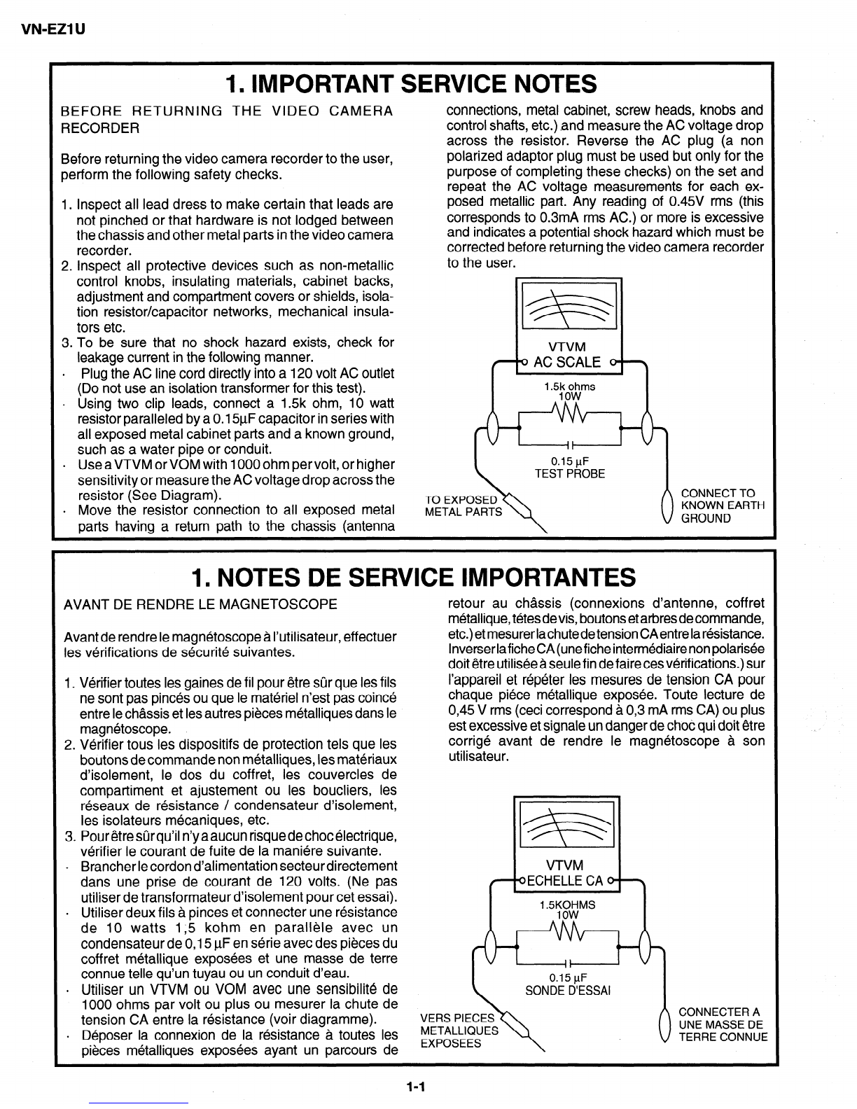
3. To be sure that no shock hazard exists, check for
leakage current in the following manner.
l Plug the AC line cord directly into a 120 volt AC outlet
(Do not use an isolation transformer for this test).
. Using two clip leads, connect a 1.5k ohm, IO watt
resistor paralleled by a 0.1$LF capacitor in series with
all exposed metal cabinet parts and a known ground,
such as a water pipe or conduit.
. Use a VTVM or VOM with 1000 ohm per volt, or higher
sensitivity or measure the AC voltage drop across the
resistor (See Diagram).
VTVM
( 0 AC SCALE 0 >
’ -5kims
. Move the resistor connection to all exposed metal
parts having a return path to the chassis (antenna METAL PARTS
1. NOTES DE SERVICE IMPORTANTES
AVANT DE RENDRE LE MAGNETOSCOPE
Avant de rendre le magnetoscope a I’utilisateur, effectuer
les verifications de securite suivantes.
1. Verifier toutes les gaines de fil pour etre sur que les fils
ne sont pas pin&s ou que le materiel nest pas coin&
entre le chassis et les autres pieces metalliques dans le
magnetoscope.
2. Verifier tous les dispositifs de protection tels que les
boutons de commande non metalliques, les materiaux
d’isolement, le dos du coffret, les couvercles de
compartiment et ajustement ou les boucliers, les
reseaux de resistance / condensateur d’isolement,
les isolateurs mecaniques, etc.
3. Pour etre stir qu’il n’y aaucun risque de choc electrique,
verifier le courant de fuite de la maniere suivante.
retour au chassis (connexions d’antenne, coffret
metallique, t&es devis, boutons etarbres decommande,
etc.)et mesurer lachute detension CA entre laresistance.
lnverser lafiche CA (une fiche intermediaire non polarisee
doit etre utilisee a seule fin defaire ces verifications.) sur
I’appareil et repeter les mesures de tension CA pour
chaque piece metallique exposee. Toute lecture de
0,45 V rms (ceci correspond a 0,3 mA rms CA) ou plus
est excessive et signale un danger de choc qui doit etre
corrige avant de rendre le magnetoscope a son
utilisateur.
I
. Brancher le cordon d’alimentation secteurdirectement VTVM
dans une prise de courant de 120 volts. (Ne pas c oECHELLECAo 3
utiliser de transformateur d’isolement pour cet essai).
. Utiliser deux fils a pinces et connecter une resistance
de IO watts I;5 kohm en parallele avec un
condensateur de 0,15 PF en serie avec des pieces du
coffret metallique exposees et une masse de terre
connue telle qu’un tuyau ou un conduit d’eau.
. Utiliser un VTVM ou VOM avec une sensibilite de
1000 ohms par volt ou plus ou mesurer la chute de
tension CA entre la resistance (voir diagramme). VERS PIECES
. Dbposer la connexion de la rbsistance a toutes les METALLIQUES
pieces metalliques exposees ayant un parcours de
1-I

VN-EZI U
WARNING :TO REDUCETHE RISK OF FIRE OR ELECTRIC SHOCK, DO NOT EXPOSE
THIS APPLIANCE TOWET LOCATIONS.
/&/AA
CAUTION: TO REDUCE THE RISK OF ELECTRIC
SHOCK. DO NOT REMOVE COVER. NO
USERSERVICEABLE PARTS INSIDE.
REFER SERVICING TO QUALIFIED SERVICE
PERSONNEL.
A This symbol warns the user of uninsulated
voltage within the unit that can cause danger-
ous electric shocks.
n
1 This symbol alerts the user that there are
important operating and maintenance instruc-
0 tions in the literature accompanying this unit.
CAUTION
This symbol mark means following.
For continued protection against fire haz-
ard, replace only with same type fuse.
(F901; 1.75A 24V, F902; 1.75A 24V,
F903; 1A 24V, F904; IA 24V, F905; IA
24V)
ATTENTION: POUR REDUIRE LES RESQUES D’INCENDIE OU DECHOC ELECTRIQUE,
NE PAS EXPOSER CET APPAREIL A LA PLUIE OU A L’HUMIDITE.
RISQUE DE CHOC ELECTRIQUE
NE PAS OUVRIR n
1
0
ATTENTION: AFIN DE REDUIRE LES RISQUES DE
CHOC ELECTRIQUE, NE PAS RETIRER LE
COUVERCLE, AUCUN ORGANE INTERNE
NE PEUT ETRE REPARE PAR
L’UTIUSATEUR, CONFIER L’APPAREIL A
UN DEPANNEUR QUALIFIE.
A Ce symbole signale a I’utilisateur la presence
d’une tension non isoleea I’interieurde I’appareil
qui peut etre la cause de secousses electriques
dangereuses.
nCe symbole avertit I’utilisateur que des in-
1 structions importantes relatives a I’utilisation
et al’entretien se trouvent dans le manuel
0 accompagnant I’appareil.
ATTENTION
Ce symbole signifie que I’on devra uti-
liser un fusible de meme type (F901;
1.75A 24V, F902; 1.75A 24V, F903; IA
24V, F904; 1A 24V, F905; IA 24V) pour
assurer la securite. A
1-2

VNkEZlU
2. SPECIFICATIONS
MPEG-4 Digital Recoder
Power requirement:
Power consumption:
Record format/Image compression system:
Sound recording system:
Pixel composition:
Recording medium:
Photometry:
Exposure control:
Pickup device:
LCD Monitor:
Lens:
Focus range:
White balance:
Shutter speed:
Self-timer:
Microphone:
Speaker:
Operating temprature:
Storage temprature:
Operation humidity:
Dimentions:
Weight:
Supplied SmartMedia Card
Memory capacity: 4MB
Memory type:
Power requirement:
Operating temprature:
Storage temprature:
NAND flash EEP-ROM
3.3 v
O°C to +4O”C (32°F to 104°F)
-20°C to +6O”C (-4°F to 140°F)
DC6V
[Recording] 3.4 W
[Playback] 2.7 W
[Movie] MPEG-4/ASF
[Still] JPEG base line conformance/JPEG (Exif 2.1)
ADPCM, monaural, 8 kHz sampling
[Movie] 160 x 120 pixels/320 x 240 pixels
[Still] 640 x 480 pixels (square dots)
SmartMedia card (SSFDC) (3.3 V) (2MB, 4MB, 8MB, 16MB, 32MB)
TTL center-weighted average metering
Aperture-priority auto exposure
l/4-inch square pixel color CCD image sensor (with approx. 350,000 pixels
including optical black) progressive scanning
1.8 inch color screen with approx. 61,000 pixels
Fixed focus with macro positon, F=3.4/8 f=3.8 mm
[Normal] t-A approx. 24” (60 cm) to 00
[Macro] aapprox. 4” (10 cm)
Automatic tracking, manual switching (“OUTDOOR”/“INDOOR”)
Auto variable
[Movie] l/l 5 to l/4000 second
[Still] l/4 to l/4000 second
IO second
Monaural nondirectivity
020 mm 100 mW output (monaural)
O°C to +4O”C (32°F to 104°F)
-20°C to +6O”C (-40°F to 140°F)
30% to 80% (with no dew formation)
37/32”(W)x 317l$‘(H) x 1*‘/32”(D)
[81.4 mm (W) x 89.5 mm (H) x 42 mm (D)]
0.33 Ibs (148 g) [body only]/053 lb (240 g) [including a SmartMedia card,
four AA-size alkaline batteries and a hand strap]
AC Adapter (UADP-0243TAZZ)
Power requirement: AC 11O-130 V/60 Hz,
DC output: DC 6.0 V/700 mA
Operating temperature: O°C to +40°C (32°F to 104°F)
Storage temprature: -20°C to +6O”C (-4°F to 140°F)
Dimensions (approx.): 23/8”(W) x 33/8”(H) x 1*‘/32”(D)
[60 mm (W) x 86 mm (H) x
49 mm (D)]
Weight (approx.): 1.08 Ibs (490 g)
Specifications are subject to change without notice.
* Minimum ilumination: Since there is no widely accepted testing procedure for determining minimum illumination
capability, lux ratings are comparable only between models from the same manufacturer.
Alkaline batteries
(AA-size x 4) Hand strap Soft case PixLab Integrated Digital
Media Software CD-ROM
3.3 V type
SmartMedia (4MB) SmartMedia holder Index label (X 2) Write-protect seal (x 4)
ACadapter
UADP-0243TAZZ
Floppy disk adapter for med’iaTM
VR-1FPN
RUNTK0350TAZZ

3. PART NAMES
For details on the use of each control.
VN-EZl U
Lens body --i 1
(CAME RA/PLAY
POWER
LCD monitor
Iris select switch
Shutter button
Focus (Macro/Normal) select switch
Lens
Mode select switch
(MOVIE/STILL select switch)
Operation button
MENU button
.
Grip
L_.---- Hand strap loop
r Lens body
(CAMERA/PLAY select switch)
Microphone
Speaker
DC IN 6V terminal
-Tripod socket
- SmartMedia slot
3-1

VN-EZl U
4. DISASSEMBLY OFTHE SET
*For assembly, tighten the screw to the torque of 0.5+0.1/-O kg cm.
*Previouslv remove the smart medium unit.
1.
Batter J
B
Remove the screws (@ LX-BZ021 OTAFN)(1PCS.) and (@ LX-
HZOQ56TAFN)(l PCS.)and (@LX-BZO208TAFN)(3pcs.).
Open the battery lid as instructed with 0.
Remove the front cabinet, lifting it as instructed with 0.
Is unit
@Tapping
b
.
Remove the screws (@ LX-HZ0056TAFN)(l PCS.)and (@I LX-
HZ0062TAFF)(4pcs.).
. Lift the lens unit, and remove the CCD flex and tilt connector
across the main PWB.
l Remove the operation key flex connector and SP microphone
connector, and lift the main PWB.
3.
. Remove the screws (@LX-BZO208TAFN)(7pcs.).
4.
. Remove the screws (@LX-BZO208TAFN)(2pc.).
. Remove the CCD flex.
5.
Q
G
. Remove the CCD PWB.
6.
. Remove the screws (
HZ0206TAFN)( 1PCS.). 8TAFF)(2pcs.) and (t@LX-
. Pressing the power PWB to prevent it from floating, lift the main
PWB in the arrow direction. (Take care that the board-to-board
connector is slightly inner than the center.)
. Remove the screw (OLX-HZ0058TAFF) of the shutter PWB,
and the main PWB will be removed.
7.
ery connector
Back lig
connect PWB FFC
JACK PWB
. Remove the JAK PWB screw (0 LX-HZ0062TAFF)(l PCS.),the
battery connector, TFT PWB FFC and back light connector, and
the power PWB will be removed.
Note: As far as the power PWB is routed to A, connect the black lead
wire of the jack PWB directly to the battery terminal. From A, solder two
lead wires
from the battery terminal to the power PV’!/Band the black lead wire from
the jack PWB to the land near the battery connector.
8.
. Remove the screws (@%BZ0208TAFN)(3pcs.).
. Remove the TFT flex. _p TUT
. Pull off TFT in the arrow direction.
IO.
PWB
/. Remove the screw (6 LX-BZ0208TAFN), and TFT PWB will be
1 removed.
4-I

VN-EZl U
4-1. CAUTION ON ASSEMBLY
I. Caution for wiring treatment of rear cabinet
l Check whether the flexible and lead lines framed with ()
in the left figure swell out or not.
Fig. 1. Rear cabinet (Whole)
Tripod base holder
2. Cauti
Fig. 2. Rear cabinet (Bottom)
l Check whether the insulation tape is peeled off on the base
holder of the tripod framed with (-) in the left figure or
not.
l Take care to prevent the rear cabinet framed with ()
in the left figure from being outside the front cabinet.
Fig. 3. Rear cabinet (Side face)
l Take care to insert the projection of the front cabinet
framed with (-) in the left figure into the area (~ in
thefigure below) between the rear cabinet and tripod base
holder.
Tripod base holder
Fig. 5. Rear cabinet (Bottom)
4-2

VN-EZl U
5. TEST MODE
The camera has two kinds of the test mode functions, mode 1 and mode 2, which
5-l. HOW TO ENTER INTO THE MODE 1 (INITIAL SCREEN
Mode for setting the CSD display language, clock display and so on
1) Pressing the A key and MENU key, turn on the POWER switch.
f - ‘I
) c-a_:+ ~ I+ pg$T
‘.Z. ::::::::::::: .:::
. ..~.Qq$:
I
2) After BUSY is displayed, the initial w J
screen of Mode 1 is displayed.
Initial screen of Mode 1
are used for development/production/service.
OF MODE 1)
5-l-l. Changeover of OSD display language and clock display (linked)
1) Select COUNTRY with A or ‘I key, and select the country display with 4 or ) key.
2) Select NORMAL SET with A or v key, and determine it with ) key.
3) End the setting with POWER OFF.
Country OSD language Clock display
displav displav Year(Y). Month(M). Dav(D) 1 Time
JP 1 Japanese 1 YYYY. MM. DD 1 AM 12:OO 1
us I Enalish 1 MM. DD. YYYY 1 12:OOAM 1
UK 1 Enalish 1 DD. MM. YYYY 1 12:OOAM 1
12 o’clock at the daytime is 12:00PM,
and 12 o’clock at thenighttime is 12:OOAM.
EU English DD. MM. YYYY 0o:oo
In 24H display, 12 o’clock at the nighttime is
0o:oo.
* 12H display can be selected for user-set clock
timina.
Note: When the country display is changed, apply “clock timing” in the user setting mode.
5-l-2. Changeover of power save ON/OFF
1) Select P-SAVE with A or v key, and select ON/OFF with 4 or) key.
Setting
P-SAVE ON
P-SAVE OFF
Function
Auto power-off is set unless anything is set for approx. 3 minutes.
Auto power-off is set.
2) Select NORMAL SET with A or v key, and determine it with ) key.
3) End the setting with POWER OFF.
5-l-3. Return of user setting to default setting
Any other user setting except OSD display language setting (Item 5-I -1) is all returned to the default setting.
1) Select DEFAULT SET with A or v key, and determine it with ) key.
2) End the setting with POWER OFF.
5-2. MODE 2 (INSPECTION/ADJUSTMENT MODE)
[Note]: Since the data of EEPROM is rewritten if any address is selected and the data is changed, not only
carefully operate it but also be sure to record the address and data before setting the data.
Objects, meters and jigs/tools necessary for inspection and adjustment
AC adapter *Jig/tool name Part code
Separately available (VR-1 AAW) Price code
BB Remarks
Halogen light x 2 PCS.
Gray scale chart
Siemens Star Chart
llluminance meter (o-3000 lux)
Color temperature meter (1600~400000K)
Color temperature conversion filter (3200+68OOK)
1 HOYA”LB-165” I
Commercially available
JiGCHART-
JiGCHART- 1
JiGMETER-
JiGMETER-
JiGHOYA-LB165 I
CP
CE
CT
FF
BH I
Extension cable 30pin, Main (CN204) - Power (CN906) QCNW-1948TAZZ BS New
Extension cable lOpin, Main (CN202) - Control (CN2901) QCNW-1949TAZZ AP New
Extension cable 13pin, Main (CN31) - CCD (CNl) QCNW-1950TAZZ AP New
Extensioncable %in~P~~(~%7~ wT(CN803) - - -QCNW_19~TAZ~ - - - - -AK - - - New -
5-I

How to enter into the test mode (initial screen of TEST MODE)
1)
2)
3)
4)
Pressing the V key and MENU key, turn on the POWER switch.
When BUSY is displayed on the screen, release the V key and MENU key, and
the initial screen of the test mode will be displayed. (Refer to the center of the
following figure.)
Shift to each mode with the operation button of the main unit.
After setting is completed, press the MENU key, and it will return to the initial
screen of the test mode. Then turn off the power.
Color bar pattern
Screen of EEPROM SET
/
W/Y/Cy/GIMglRIBluelBlack
t
n
0
a 0 ‘I>
..:‘.
v
POWER-
+ m
Initial screen of TEST MODE Initial screen of EEPROM INI
Version display +
Screen of WB ADJ
5-2-l. Method of displaying the test pattern
To inspect and adjust the liquid crystal the color bar and monochrome pattern can be displayed.
mMethod of displaying the color bar (75% modulated)
1) The initial screen of the test mode is displayed.
2) Press the A key to display the color bar.
3) Press the MENU key, and it will return to the initial screen of the test mode. Then turn off the power.
mMethod of displaying various patterns
1) The initial screen of the test mode is displayed.
2) Press the 4 key to display EEPROM SET screen.
3) Press the 4 key to display Address 1FE of EEPROM.
4) Press the A key to set 00 as the data of Address 1FE.
5) Press the A or V key to vary the data, and the patterns in the following table will be displayed.
Address (h) Data (h)
01
02 White signal 40% Display pattern
I
1 White s&al 100%
I 03 1 Black signal I
IFE 1 04 1 Color bar signal I
05 Red signal:The signal level is the same as that of the color bar. J
I 06 1 Green signaLThe signal level is the same as that of the color bar. I
i 07 I Blue signal:The signal level is the same as that of the color bar. I
6) Set FF as the data of Address IFE of EEPROM.
7) Press the MENU key, and it will return to the initial screen of the test mode. Then turn off the power.
5-2

5-2-2. Method of selecting VALID/INVALID of the battery lid switch
For disassembly and operation, set the switch of the battery lid at VALID.
1) The initial screen of the test mode is displayed.
2) Press the 4 key to display EEPROM SET screen.
3) Select Address 1FD with 4 or ) key, and set FF as the data with A or v key.
4) Press the MENU key, and it will return to the initial screen of TEST MODE. Then turn off the power to complete the setting.
Since the battery lid switch becomes invalid, it can be disassembled for inspection and repair.
[Note]: After the inspection and repair are completed, be sure to return the data of Address 1FD to 00 (except FF), and turn the battery
lid switch to VALID.
5-2-3. Method of adjusting the LCD display
For adjustment, remove TFT PWB from LCD unit.
a) Horizontal position adjustment
1) The initial screen of the test mode is displayed.
Select Address 1FE with 4orb key, and set the data at 04 with
the wh ite and black bars at both ends of the color bar displayed
+To POWER PWB
I I
L-l-, v
JTo POWER PWB
4) After adjustment, set FF as the data of Address 1FE with A or v key.
5) Press the MENU key, and it will return to the initial screen of TEST MODE. Then turn off the power to complete the setting.
b) Common bias adjustment
[Note]: Apply this after aging of approx. 5 minutes. The back light set by the user is regarded as standard.
1) The initial screen of the test mode is displayed.
2) Press the 4 key to display EEPROM SET screen.
3) Select Address 1FE with 4 or ) key, and set 00 as the data with A or v key.
4) Bring the lens unit into the shooting state (EE display).
5) Select Address 1F8 with 4 or ) key.
6) Shoot the gray scale, and vary the data with A or v key to find such a point as the black sinks to the deepest.
7) After adjustment, select Address 1FE with 4 or ) key, and set FF as the data with A or v key.
8) Press the MENU key, and it will return to the initial screen of TEST MODE. Then turn off the power to complete the setting.
c) White balance adjustment
[Note]: Apply this after aging of approx. 5 minutes. The back light set by the user is regarded as standard.
1) The initial screen of the test mode is displayed.
2) Press the 4 key to display EEPROM SET screen.
3) Select Address 1FE with 4 or ) key, and set 01 as the data with A or v key.
(White 40% pattern is displayed.)
4) Bring the sensor unit of the color thermosensor into contact with the screen of
the LCD monitor, and measure the color temperature (M) and.compensation
value (CC).
[Note]: To prevent the LCD monitor screen from being injured at this time,
don’t press the sensor unit of the color thermometer or rub it.
To gain the color temperature of 7600 +_200K and the compensation value of 50 +_2, select Address 1F5 or 1F6 with 4 or ) key, and
adjust the data with A or v key.
[Note]: Take the measurement 2 or 3 times to reduce the error.
Select the dark place to prevent an excess light from entering the sensor unit of the color thermometer.
First adjust the color temperature into the standard range, and adjust the compensation value (CC).
5-3

Color temperature
Low Compensation value
Low Address 1F5 (B) 4 Address 1F6 (R) )
‘IDown Fixed
High Low Fixed VDown
Low High Fixed I AUP I
High
Low High
Within standard AUP
VDown Fixed
AUP
High
Within standard Within standard
Low AUP VDown
VDown VDown
Within standard
Within standard High
Within standard AUP
Adjustment end AUP
Adjustment end
5-2-4. EEPROM INI (initial) method
Apply this when EEPROM is replaced or the version of the microcomputer is increased.
nAdjustment preparation and check items
Before entering the initial screen of the test mode, insert the smart medium in which data is already written.
Moreover, check the version. Initial screen of TEST MODE
Version display +
Screen of EEPROM INI (PRO) Screen of EEPROM INI Screen of EEPROM INI (ALL)
VN-EZl U
a) PRO (protect) mode
Rewrite the other data except the white balance setting, TFT setting and clock with the data in the smart medium-l) The initial screen
of the test mode is displayed.
1) The initial screen of the test mode is displayed.
2) Press the ) key to display EEPROM INI screen.
3) Press the 4 key to display INI (PRO) screen.
4) Press the shutter button to rewrite the data with the data in the smart medium.
In approx. 1 second, it will automatically return to EEPROM INI screen.
5) Press the MENU key, and it will return to the initial screen of TEST MODE. Then turn off the power to complete the setting.
6) Perform steps in “5-l-2. Return of user setting to default setting”.
7) Then turn off the power to complete the setting.
b) ALL mode
Rewrite all data of EEPROM with the data in the smart medium.
1) The initial screen of the test mode is displayed.
2) Press the ) key to display EEPROM INI screen.
3) Press the ) key to display INI (ALL) screen.
4) Press the shutter button to rewrite the data with the data in the smart medium.
In approx. 1 second, it will automatically return to EEPROM INI screen.
5) Perform steps in “5-2-3. Method of adjusting the LCD display” and “5-2-5. Camera (CCD white balance) adjusting method”.
6) Press the MENU key, and it will return to the initial screen of TEST MODE. Then turn off the power to complete the setting.
7) Perform steps in “5-l-2. Return of user setting to default setting”.
8) Then turn off the power to complete the setting.
*Use the smart medium, FD adaptor or PC card which is copacked or optional.
5-4

5-2-5. Camera (CCD white balance) adjusting method
Preparation and check items before adjustment
For illumination, apply the approximation of the color temperature 3200K and illuminance 3000 lux, and the light source of 2 or more
lamps are preferable for the even illumination.
Use the chart which is not stained or discolored.
Initial screen of TEST MODE
1 MENU
Screen of WB ADJ
I
I
, During adjustment Adjustment end I
(CMP-ADJ) 1
I
i
I
i
I
i
Press the ) key for changeover.
(AUTO)position is used for
investigation but not used for
the service.
1) The initial screen of the test mode is displayed.
2) Press the V key to display WB ADJ (3200) screen.
3) Shoot the gray scale chart.
4) Press the shutter button, and wait until CMP-ADJ is displayed.
5) Press the ) key to display WB ADJ (6800) screen.
6) Set up the color temperature replacement filter (LB-165 3200K -+ 6800K conversion) in front of the lens.
7) Press the shutter button, and wait until CMP-ADJ is displayed.
8) Press the MENU key, and it will return to the initial screen of TEST MODE. Then turn off the power to complete the setting.
5-2-6. Lens back focus adjusting method
Preparation before adjustment
Remove the front cabinet of the main unit, and remove the cabinet of the lens section.
(The cabinet of the lens section can be disassembled or assembled only when the front
cabinet of the main unit is removed.)
Remove the macro adjusting ring. (Refer to the right figure.)
Remove two tilt holder fastening screws on the main unit side, and holding the tilt
section and CCD PWB section with left hand, pinch both ends of the macro adjusting
ring with right hand, and gradually pull it up in the arrow direction. (At this time, take
care to prevent missing the macro ring fastening hardware.)
During adjustment, keep the front cabinet of the tilt holder main unit and the rear
cabinet of the camera in the assembled state, and the main unit will be stabilized.
[Note]: Take care to prevent applying a forcible force to the tilt section. I Tilt holder fastening screw position
5-5

I_L Distance of objet t :1000&l
Barrel section
Adjusting method
1) When shooting, align the center of Siemens star chart to that of the motor screen.
2) Turning the barrel section of the lens with finger, adjust the lens focus to be the best, checking the monitor screen.
3) Align the macro adjusting ring to the position (level the notch rightward) in the figure below, and straightly insert the barrel from
the front side without moving the barrel.
Macro ring fixture
Hole Dosition of macro adjusting ring and CCD PWB
y Macro adjusting ring
4) Insert the macro ring fixture into the macro adjusting ring.
Check after adjustment:
Verify that the object is focused in the range of 45 cm to near the infinite point.
5) Assemble the cabinet. Align the macro switch knob of the cabinet to normal, and make an assembly by inserting the inside switch
lever to the notch of the macro adjusting ring.
[Note]:
@Before assembly, verify that the lens and cabinet inside are not stained.
lWhen assembling the front cabinet of the lens section, the focus switching knob must be positioned at the ordinary shooting position.
l When assembling the front cabinet of the main unit, take care to prevent pinching FPC which is present between CCD PWB and
main PWB.
5-6

VN-EZl,U
Objects, instruments and jig/tools necessary to serve
l Gray scale chart
l Color bar chart
l Halogen lamp: 2 PCS.
l Illumination meter
l Color temperature meter
l Color temperature conversion filter
HOYA “LB-1 65”
l Color video monitor
l Extension cables
lrl
8
L IO
TILT PWB
Smart Media Socket
fY
To video
monitor I1 jIl.
TFT PWB TFT Unit
SP Mic
CCD PWB JACK PWB
CONTROL PWB SHUTTER PWB
POWER PWB
Service of camera section
NO 1
. Name I Part No. 1 Code 1 Configuration 1 Note
1 Gray Scale Chart (390 x 520 mm) JiGCHARA-1 CP
2 Color bar chart (240 x 320 mm) JiGCHART- DA
3 Illumination meter (0 to 3000 lux) JiGMETER-
(1600 to 400000 degrees K) JiGMETER-
5 Color temperature conversion filter
(3200 degrees K a 6800 degrees K)
JiGHOYA-LB165 BH
6 Siemens star chart JiGCHART- 1 CE
7 Torque driver (1.5kg.cm) JiGTD1500RTDH CB
8 MAIN PWB (CN204) - POWER PWB (CN906) 30pin QCNW-1948TAZZ BS
9 MAIN PWB (CN202) - CONTROL PWB (CN2901) IOpin QCNW-1949TAZZ AP
IO 1 POWER PWB (CN907) - TFT PWB (CN803) 13pin IQCNW-1950TAZZ 1 AP 1 I
Note:
1. The color temperature conversion filter (jig name No. 5) is available from Hoya Kogaku in your district.
5-7

rl
I Ja&laAu(
k I I I I
Jaj_4aAuoz
3ana I I I
80L6W
LO6-31
JaMOd
:.:
:::
.:_
IL
::: /wa IJL L Y J
:::
:.:
::. 1’11\ 1
I
i
i
i
i
i
..I.
....
is
.:.:
I:!:
I, ~._rnl,
:::: w
....
::::
::::
;:;:
.:.:
::::
::::
.-1;
::::
>;.
ii;
1.1. .I._
.i.
:::: b
$
....
....
ig
$5
:i:: -a 31w
I . . . . . . . . . . . . ,
.
:
.
.m
Ma 6u!pni~u!)
J8pOXl~ Oap!/\ tl
Ii/l
ma03
ZZVl869OXI
soz-31
~a~ndumom!w
;_
VlO%LO
zoz-31
wvtiaw91
l-/9lLLWSWIHA
z09-3l=Po~ =!oA
twwooz
Gu!pnpu!)
6uqsaaoJd
ieu6!sa33
> ZZbOOLOXI-Htl 101-31
31s~ 6u!ssaaoJdp~6~s
.*
t:
. I(luo 6u!~ooysa!/\oyy2:; :. 5.
............................
tju!~ooysa!AOw I
f ,...........................A yxqhld a6txu! ~pgs/a!~oyy fjiiiii;i&.jg’ )
‘0: ................... 8 6u!9ooys a6eu4 ~lgs/a!~op,j (?%~i6ii~~mi j.~eya MO14 IT&!S
..................
. .
v l.;

VN-EZl U
7. OSCILLATOR, DIVIDING AND MULTIPLY MAP
CCDICDSIAD
12.2727
MHz
ASIC
[ 0sE-j
I I
443s -f I I
l/2 l/7 x3 l/70 l/3068
D&K P&K CL P_SCNC D&K
I + 4 4 +
DSP ‘t
I
73.6362
MHz
Microcomputel
3.506486
MHz
8. POWER CONTROL FLOW
ON
I
0.8s 10.6s 1
power SW I
Unless pressed 0.5 see or more,
it will not be turned on. (Prevention of wrong operation)
PCNTl I
DC-DC converter ON (Microcomputer ON)
PCNT2 I
CircuitON
BLCNT I
Back lightis lit.
Whenbattery lid isopened,it willbe turned off here.
SD-RAM
I I
DC-DC
73.6362 350kHz
X801
TFT control
IR3R29M I
Terminal name Battery(V) Measurement terminal
PCONTI 3.3 CN906-10 TL949
PCONT2 3.3 CN906-13 TL952
BLCNT(normal) 3.3 CN906-30 TL973
+5V (CCD)
+I 5V (CCD)
-9V (CCD)
+B (Audio)
+3.3V (MEDIA)
5 CN906-1 TL917
15 CN906-2 TL921
-9 CN906-3 TL925
6 CN906-4 TL929
3.3 CN906-5 TL933
+3.3V (RTC) 3.3 CN906-6 TL937
+3.3V(LSI) 3.3 CN906-7 TL941
+2.5V (LSI) 2.5 CN906-8 TL944
+2.5V (LSI) 2.5 CN906-9 TL945
-15V (TFT) -15 CN907-7 TL975
+7.5V (TFT) 7.5 CN907-8 TL979
+I 5V (TFT) 15 CN907-9 TL983
+5V (TFT) 5 CN907-IO TL987
7-1

9. TROUBLESHOOTHING
POWER CIRCUIT TROUBLESHOOTHING
The power cannot be turned on.
Check SW901. I
Isvoltage output between the pins (2), No
(3) (6) and (7) of Q921 and TL1922?
l Check battery and AC adaptor.
Check battery terminal.
Yes Check F901 and F902.
Is OV applied to the pin (13) of IC901 No B Check periphery of Q924. Check SW291 1.
when power is turned on? Is PCNTl at Hi level?
Yes Check microcomputer circuit.
Is triangular wave of approx. 700 mVp-p No l
Check C906, R902 and R905.
output at the pin (17) of IC901? Check C903 and R910.
Yes
Is voltage supplied to the emitter of ‘No Check F903, F904 and F905.
Q930, Q906 and Q907? l Check L904 and D906. 1
Yes
Is 3.3V output to TL943? No Shorted load of 3.3V line.
Yes l Check Q906, D905, L905 and pins (8)
and (9) of IC901.
v
Is 2.5V output to TL944? No Shorted load of 2.5V line.
a Yes l Check Q928 and IC903.
L l
Is 5.OV output to TL919 and TL989?
Yes
Shorted load of 5V (CCD) and 5V (TFT) line.
Check IC904, Q930, Q911, IC906, Q908, D906,
L911, L904 and pins (11) and (12) of IC901.
Shorted load of 3.3V (MEDIA) line.
Is 15V applied to TL923 and TL983?
Is 7.5V applied to TL981?
Is -9V applied to TL927?
Is -15V applied to TL977?
No l Shorted load of 15V (CCD), -9V (CCD), lSV(TFT),
7.5V (TFT) and 15V (TFT) line .
Check Q907, T901, 0907,0908, L907, L908, L909,
L910 and pins (15) and (16) of IC901.
Is back light lit? Does T903 oscillate?
I Yes
No 1
+ Check Q922, Q923, Q925,
Q929, L913 and C946.
IC205 TROUBLESHOOTHING
Is the terminal (21), (28), (32) (33) (47) No -, Check power circuit.
(48) (50) (82)s GND, (9), (29) (34) (35) Check L208.
(40) (49) (77) or (79) of microcomputer
power [3.3V] is normal.
RSTX(75)“H” Check IC204 and D201.
Is clock (approx. 4 MHz) supplied to pin No b Check IC201 oscillation.
(80)? (24.5454MHz)
I Yes
l
&eoi;ration keys (36) (37) and (38) No b Check relevant key.
Check R2901 -R2908 and R291 O-R291 2.
Check connection lines of IC205 and lC206.
I Yes
*
Is IC2901 communication normal? No Check connection lines of lC205 and lC2901.
l Check IC2901 for oscillation (32 kHz).
I I Yes I I - . r I
l
Is IC201 communication normal?
I Yes
No b Check pins (l), (2), (99) (loo), (83)-(90)
and periphery of IC201.
No + Check pins (91)-(98), (83)-(90) and
periphery of IC203.
Defective IC205. Short circuit of each pin.
1IC205 normal.
Yes
CCD TROUBLESHOOTHING
1Turn mode SW to MOVIE.
No
1Is power voltage no-1 d Refer to the troubleshooting of the
I . I Yes
+
I 1power supply. I
Is clock signal supplied to TL15, TL16 No l
Check IC35 and periphery of IC201.
and TL17? Check CCDFPC.
I Yes
Is pulse signal supplied to TLG-TLlO? No b Check IC31 and its periphery.
Check CCDFPC.
Yes
Is signal supplied to (l)-(4) and (12)- Check ICl peripheral circuit. I
(141 of Cl?
b48 or LCD unit is defective. 1
ICl is defective.
Check Ql.
CCD unit is normal.

CAMERA TROUBLESHOOTHING AUDIO TROUBLESHOOTHING LCD TROUBLESHOOTHING 7
Abnormal
Picture is not displayed.
I
1Turn mode SW to MOVIE.
LNo _
Is LCD monitor normal? -b Refer to the troubleshooting of the
Is OSD output? LCD supply.
No r
l Refer to the troubleshooting of the
CCD supply.
Is the terminal (12) (17), (33), (39), No Check IC33, L31 and R44.
(40) (42), (43) or (44) of power [3.3V] b
of IC34 normal?
Check CCDFPC.
Is clock signal supplied to (16), (21) No Check IC201 peripheral circuit.
and (22) and pulse signal supplied to
(20) and (23)? I
Turn mode SW to MOVIE.
(Shooting mode)
b Refer to the troubleshooting of the
power supply.
Is the voltage of approx. 2 V output to
TL604? Check R650 and R651.
I Yes
v
Is signal output at pin (25) of IC602 No Check pins (24) and (25) of IC602,
when normal microphone is connected l and Q652, Q653, FB603, FB604 and
and signal is supplied? their periphery.
I Yes
Is signal supplied to (18) and (20) of Check IC201 and their periphery circuit.
IC602.?
Are pins (1l), (13) and (14) of IC602
properly connected to IC205? No b Check IC205 and their periphery.
Yes
-No
Is approx. 1.OV voltage supplied to b Check connection line of IC205. IC602 is defective.
Is output signal output to A/D output
(2)-( 11)? IC34 is defective. Check IC201 and their periphery. 1
Yes
Is signal output at pins (4) and (6) of No b Check the pins (4) (5) and (6) of fC602
IC602? , as well as R604 and R605.
1IC201 is defective. 1 Check C603 and R603.
Is the signal output to TL601 and
TL602? Check IC601, its periphery, FB601 and
No
i ’ FB602.
Yes
1Check the speaker.
Is back light lit? Refer to the troubleshooting of the
power supply.
Is -15V supplied to TL849, 7.5V to No Refer to the troubleshooting of the
TL853,15V to TL857 and 5V to TL860? b power supply.
I Yes Check TFT FPC.
+ No
ISvideo signal suppm1 + Check IC201, its periphery and Q201.
I Yes Check TFT FPC.
+-No
Are 6 to 9V common signals output at b Check IC802 and their periphery.
TL824 and TL868?
I Yes
Is approx. 2.4V signal output at pin (2) No + Check IC806, its periphery, and IC806
of IC806? to IC205 connection.
Yes
1IS IC801 oscillated at No d Check lC801 and X801. 1
I Yes
Is signal output at TL831, TL832 and Check IC801.
TL833? I
1
Yes
1Defective LCD unit or FPC wire breakaae I
Medium is not read.
I Yes
Defective medium
1
Yes
Formatting with PC
I Yes No + Check the smart medium socket, lC201
and its periphery.
No
Medium normal.

VN-EZI U
10. IC FUNCTION LIST (IC205:IXO698TA)
Micom Pin No. Micom Port Name I/O Signal Name RST ACT Function/Connection block
1 P22 0 PRO VCAM
2 P23 I PBUSY VCAM
3 P24 0 DSPRESET L H DSP reset output
4 P25 0 CCDCNT L H CC0 power circuit
5 P26 0 PCNTI L H Power circuit
6 P27 0 PCNT2 L H Power circuit
7 P30 0 BLCNT H L TFT back light power
8 P31 I PWMODE L Power SW detection (Low)
9 vss
IO P32 I LENSSW Lens direction detection (Low: Playback)
11 P33 I TFTINVSW TFT inversion detection (Low: Reverse)
12 P34 I/O RTCDA RTC data input/output
13 P35 0 RTCCL RTC clock
14 P36 0 PO Camera circuit power control (Low: Playback)
15 P37 I SHTR Shtter input (Low)
16 SIN0 I SIN RS232C data input
17 SOT0 0 SOT RS232C data output
18 P42lSCKO
19 P43 I/O EDAT/ESDA EEPROM
20 P44 0 TFTINVO TFT inversion setting output (Low: Reverse)
21 vcc
22 P45 0 ESHIFT/ESCL EEPROM
23 P46 I ACDTCT AC adaptor detection
24 P47 0 Open drain output
25 P70/SDA Open drain output
26 P71/SDA Open drain output
27 P72 Open drain output
28 DVRH DA converter external reference power terminal
29 DVSS DA converter power terminal
30 DA0 0 AGCI Camera circuit
31 DA1 0 AGC2 Camera circuit
32 AVCC AD converter power terminal
33 AVRH AD converter external reference power terminal
34 AVRL AD converter external reference power terminal
35 AVSS AD converter power terminal
36 AN0 I KEY1 Operation unit
37 AN1 I KEY2 Operation unit
38 AN2 I MODE Operation unit (Static picture/dynamic picture)
39 AN3 I BATT Power voltage detection
40 vss
41 AN4 I PWERR Power short circuit detection
42 AN5 I TEMP Temperature detection
43 AN6
44 P57/AN7
45 IRQO I PINT VCAM
46 P81/IRQl
47 MD0 I MD0 H:Single chip operation mode specification
48 MD1 I MD1 H:Single chip operation mode specification
49 MD2 I MD2 L:Single chip operation mode specification
50 TEST I H fixed
51 P82/l RQ2 0
52 P83/l RQ3
53 P84 0 BLCH TFT brightness switch (Low: Dark)
54 P85 0
55 P86/0UT3
56 NC Open terminal
57 P60 0 DEN AUDIO codex (DataEnable)
58 P61 0 COIN AUDIO codex (ContolDataln)
IO-I

VN-EZl’U
Micom Pin No. Micom Port Name I/O Signal Name FIST ACT Function/Connection block
59 * P62 0 DCLK AUDIO codex (DataShift)
60 PPGOO 0 BEEP AUDIO codex (PWI)
61 P64 0 PDN AUDIO codex (PowerDown)
62 P65 0 DSPPO DSP boot selection
63 P66 0 DSPPI DSP boot selection
64 P67
65 P90 I CD SSFDC
66 P91 I LVD SSFDC
67 P92 0 PRTCTO L H SSFDC
68 P93 I MEDIA Lid open detection (High : OPEN)
69 P94 I PRTCTI SSFDC soket (Low : protect)
70 P95/ZlNl 0 XRST Reset output (VCAM)
71 P96/lNO 0 TFTXRST TFT reset output I
72 I P97/lNl I I I I I I
73 PA0 lol DADI t 1 1 DA converter data I
74 PA1 lOI DACK 1 I 1 DA converter clock I
75 RSTX I I I l Reset input terminal
76 PA2 IW DALD l I l DA converter road I
77 XOA I
78 XIA I
79 vss
80 x0 I (24.5454 + 7MHz) Clock input terminal
81 Xl
82 vcc
83 PO0
84 PO1
85 PO2
86 PO3
87 PO4
88 PO5
89 PO6
90 PO7
91 PI0
92 PI1
93 PI2
94 PI3
95 PI4
I
I/O
I/O
I/O
I/O
I/O
I/O
I/O
I/O
0
0
0
0
I
DBO
DBI
DB2
DB3
DB4
DB5
DB6
DB7
DSPHCS
DSPHAO
DSPHAI
DSPHRD
DSPHRE
DSPNCAM data bus
DSPNCAM data bus
DSPNCAM data bus
DSPNCAM data bus
DSPNCAM data bus
DSPNCAM data bus
DSPNCAM data bus
DSPNCAM data bus
DSP
DSP
DSP
DSP
DSP
r 96 PI5 1 0 1 DSPHWR 1 1 1 DSP I
97 PI6 1 I 1 DSPHWE 1 1 1 DSP I
98 PI7
99 P20
100 P21
0 DSPHINT4 DSP
0 PADREN VCAM
0 PWR VCAM
1o-2
Other manuals for VN-EZ1U
4
Table of contents
Other Sharp Voice Recorder manuals