SIGNALCORE SC5412A Owner's manual

SC5412A
400 MHz to 6 GHz IQ Modulator
PXI Express Interface
Operating and Programming Manual
© 2013-2020 SignalCore, Inc.
support@signalcore.com

SC5412A Operating & Programming Manual i
CO N T E N T S
Important Information
Warranty.................................................................................................................................................1
Copyright & Trademarks ........................................................................................................................1
International Materials Declarations .....................................................................................................2
CE European Union EMC & Safety Compliance Declaration ..................................................................2
Warnings Regarding Use of SignalCore Products...................................................................................3
Getting Started
Unpacking...............................................................................................................................................4
Verifying the Contents of your Shipment...............................................................................................4
Setting Up and Configuring the SC5412A...............................................................................................4
RF Signal Connections......................................................................................................................6
Baseband Connections.....................................................................................................................7
Indicator LED....................................................................................................................................7
SC5412A Theory of Operation
Overview.................................................................................................................................................8
IF Input Section.......................................................................................................................................8
RF Output Section...................................................................................................................................9
LO Input Section ...................................................................................................................................11
SC5412A Programming Interface
Device Drivers.......................................................................................................................................12
Using the Application Programming Interface (API) ............................................................................12
Setting the SC5412A: Writing to Configuration Registers
Configuration Registers........................................................................................................................13
Initializing the Device ...........................................................................................................................14
Setting the System Active LED..............................................................................................................14
Setting the RF Frequency .....................................................................................................................14
Setting RF Input RF Amplifiers..............................................................................................................14
Setting the RF Attenuation...................................................................................................................14

SC5412A Operating & Programming Manual ii
Setting the RF Path...............................................................................................................................14
Selecting the RF Filter...........................................................................................................................14
Selecting the LO Filter ..........................................................................................................................14
Enabling LO Output ..............................................................................................................................15
Removing DC Offset in Differential Amplifiers.....................................................................................15
Setting the Output Linearity of the IQ Modulator ...............................................................................15
Storing the Startup State......................................................................................................................15
Writing to the User EEPROM................................................................................................................15
Querying the SC5412A: Writing to Request Registers
Reading the Device Temperature.........................................................................................................16
Reading the Device Status....................................................................................................................16
Reading the User EEPROM ...................................................................................................................17
Reading the Calibration EEPROM.........................................................................................................17
Calibration EEPROM Map..................................................................................... 18
Software API Library Functions
Constants Definitions ...........................................................................................................................20
Type Definitions....................................................................................................................................21
Function Definitions and Usage ...........................................................................................................21
Calibration & Maintenance....................................................................................1

SC5412A Operating & Programming Manual Rev 1.1.0 1
IM P O R T A N T IN F O R M A T I O N
Warranty
This product is warranted against defects in materials and workmanship for a period of three years from
the date of shipment. SignalCore will, at its option, repair or replace equipment that proves to be
defective during the warranty period. This warranty includes parts and labor.
Before any equipment will be accepted for warranty repair or replacement, a Return Material
Authorization (RMA) number must be obtained from a SignalCore customer service representative and
clearly marked on the outside of the return package. SignalCore will pay all shipping costs relating to
warranty repair or replacement.
SignalCore strives to make the information in this document as accurate as possible. The document has
been carefully reviewed for technical and typographic accuracy. In the event that technical or
typographical errors exist, SignalCore reserves the right to make changes to subsequent editions of this
document without prior notice to possessors of this edition. Please contact SignalCore if errors are
suspected. In no event shall SignalCore be liable for any damages arising out of or related to this
document or the information contained in it.
EXCEPT AS SPECIFIED HEREIN, SIGNALCORE, INCORPORATED MAKES NO WARRANTIES, EXPRESS OR
IMPLIED, AND SPECIFICALLY DISCLAIMS ANY WARRANTY OF MERCHANTABILITY OR FITNESS FOR A
PARTICULAR PURPOSE. CUSTOMER’S RIGHT TO RECOVER DAMAGES CAUSED BY FAULT OR
NEGLIGENCE ON THE PART OF SIGNALCORE, INCORPORATED SHALL BE LIMITED TO THE AMOUNT
THERETOFORE PAID BY THE CUSTOMER. SIGNALCORE, INCORPORATED WILL NOT BE LIABLE FOR
DAMAGES RESULTING FROM LOSS OF DATA, PROFITS, USE OF PRODUCTS, OR INCIDENTAL OR
CONSEQUENTIAL DAMAGES, EVEN IF ADVISED OF THE POSSIBILITY THEREOF. This limitation of the
liability of SignalCore, Incorporated will apply regardless of the form of action, whether in contract or
tort, including negligence. Any action against SignalCore, Incorporated must be brought within one year
after the cause of action accrues. SignalCore, Incorporated shall not be liable for any delay in
performance due to causes beyond its reasonable control. The warranty provided herein does not cover
damages, defects, malfunctions, or service failures caused by owner’s failure to follow SignalCore,
Incorporated’s installation, operation, or maintenance instructions; owner’s modification of the product;
owner’s abuse, misuse, or negligent acts; and power failure or surges, fire, flood, accident, actions of
third parties, or other events outside reasonable control.
Copyright & Trademarks
Under the copyright laws, this publication may not be reproduced or transmitted in any form, electronic
or mechanical, including photocopying, recording, storing in an information retrieval system, or
translating, in whole or in part, without the prior written consent of SignalCore, Incorporated.
SignalCore, Incorporated respects the intellectual property rights of others, and we ask those who use
our products to do the same. Our products are protected by copyright and other intellectual property
laws. Use of SignalCore products is restricted to applications that do not infringe on the intellectual
property rights of others.

SC5412A Operating & Programming Manual Rev 1.1.0 2
“SignalCore”, “signalcore.com”, and the phrase “preserving signal integrity” are registered trademarks
of SignalCore, Incorporated. Other product and company names mentioned herein are trademarks or
trade names of their respective companies.
International Materials Declarations
SignalCore, Incorporated uses a fully RoHS compliant manufacturing process for our products.
Therefore, SignalCore hereby declares that its products do not contain restricted materials as defined by
European Union directive 2002/95/EC (EU RoHS) in any amounts higher than limits stated in the
directive. This statement is based on the assumption of reliable information and data provided by our
component suppliers and may not have been independently verified through other means. For products
sold into China, we also comply with the “Administrative Measure on the Control of Pollution Caused by
Electronic Information Products” (China RoHS). In the current stage of this legislation, the content of six
hazardous materials must be explicitly declared. Each of those materials, and the categorical amount
present in our products, are shown below:
組成名稱
Model Name
鉛
Lead
(Pb)
汞
Mercury
(Hg)
镉
Cadmium
(Cd)
六价铬
Hexavalent
Chromium
(Cr(VI))
多溴联苯
Polybrominated
biphenyls
(PBB)
多溴二苯醚
Polybrominated
diphenyl ethers
(PBDE)
SC5412A
✓
✓
✓
✓
✓
✓
A ✓indicates that the hazardous substance contained in all of the homogeneous materials for this
product is below the limit requirement in SJ/T11363-2006. An Xindicates that the particular hazardous
substance contained in at least one of the homogeneous materials used for this product is above the
limit requirement in SJ/T11363-2006.
CE European Union EMC & Safety Compliance Declaration
The European Conformity (CE) marking is affixed to products with input of 50 - 1,000 Vac or 75 - 1,500
Vdc and/or for products which may cause or be affected by electromagnetic disturbance. The CE
marking symbolizes conformity of the product with the applicable requirements. CE compliance is a
manufacturer’s self-declaration allowing products to circulate freely within the European Union (EU).
SignalCore products meet the essential requirements of Directives 2004/108/EC (EMC) and 2006/95/EC
(product safety), and comply with the relevant standards. Standards for Measurement, Control and
Laboratory Equipment include EN 61326 and EN 55011 for EMC, and EN 61010-1 for product safety.

SC5412A Operating & Programming Manual Rev 1.1.0 3
Warnings Regarding Use of SignalCore Products
(1)
PRODUCTS FOR SALE BY SIGNALCORE, INCORPORATED ARE NOT DESIGNED WITH COMPONENTS NOR TESTED FOR A LEVEL OF
RELIABILITY SUITABLE FOR USE IN OR IN CONNECTION WITH SURGICAL IMPLANTS OR AS CRITICAL COMPONENTS IN ANY LIFE SUPPORT
SYSTEMS WHOSE FAILURE TO PERFORM CAN REASONABLY BE EXPECTED TO CAUSE SIGNIFICANT INJURY TO A HUMAN.
(2)
IN ANY APPLICATION, INCLUDING THE ABOVE, RELIABILITY OF OPERATION OF THE SOFTWARE PRODUCTS CAN BE IMPAIRED BY ADVERSE
FACTORS, INCLUDING BUT NOT LIMITED TO FLUCTUATIONS IN ELECTRICAL POWER SUPPLY, COMPUTER HARDWARE MALFUNCTIONS,
COMPUTER OPERATING SYSTEM SOFTWARE FITNESS, FITNESS OF COMPILERS AND DEVELOPMENT SOFTWARE USED TO DEVELOP AN
APPLICATION, INSTALLATION ERRORS, SOFTWARE AND HARDWARE COMPATIBILITY PROBLEMS, MALFUNCTIONS OR FAILURES OF
ELECTRONIC MONITORING OR CONTROL DEVICES, TRANSIENT FAILURES OF ELECTRONIC SYSTEMS (HARDWARE AND/OR SOFTWARE),
UNANTICIPATED USES OR MISUSES, OR ERRORS ON THE PART OF THE USER OR APPLICATIONS DESIGNER (ADVERSE FACTORS SUCH AS
THESE ARE HEREAFTER COLLECTIVELY TERMED “SYSTEM FAILURES”). ANY APPLICATION WHERE A SYSTEM FAILURE WOULD CREATE A
RISK OF HARM TO PROPERTY OR PERSONS (INCLUDING THE RISK OF BODILY INJURY AND DEATH) SHOULD NOT BE SOLELY RELIANT
UPON ANY ONE COMPONENT DUE TO THE RISK OF SYSTEM FAILURE. TO AVOID DAMAGE, INJURY, OR DEATH, THE USER OR
APPLICATION DESIGNER MUST TAKE REASONABLY PRUDENT STEPS TO PROTECT AGAINST SYSTEM FAILURES, INCLUDING BUT NOT
LIMITED TO BACK-UP OR SHUT DOWN MECHANISMS. BECAUSE EACH END-USER SYSTEM IS CUSTOMIZED AND DIFFERS FROM
SIGNALCORE' TESTING PLATFORMS, AND BECAUSE A USER OR APPLICATION DESIGNER MAY USE SIGNALCORE PRODUCTS IN
COMBINATION WITH OTHER PRODUCTS IN A MANNER NOT EVALUATED OR CONTEMPLATED BY SIGNALCORE, THE USER OR
APPLICATION DESIGNER IS ULTIMATELY RESPONSIBLE FOR VERIFYING AND VALIDATING THE SUITABILITY OF SIGNALCORE PRODUCTS
WHENEVER SIGNALCORE PRODUCTS ARE INCORPORATED IN A SYSTEM OR APPLICATION, INCLUDING, WITHOUT LIMITATION, THE
APPROPRIATE DESIGN, PROCESS AND SAFETY LEVEL OF SUCH SYSTEM OR APPLICATION.

SC5412A Operating & Programming Manual Rev 1.1.0 4
•Ground yourself using a grounding strap or by touching a grounded metal object.
•Touch the antistatic bag to a grounded metal object before removing the hardware
from its packaging.
•Never touch exposed signal pins. Due to the inherent performance degradation
caused by ESD protection circuits in the RF path, the device has minimal ESD
protection against direct injection of ESD into the RF signal pins.
•When not in use, store all SignalCore products in their original antistatic bags.
GE T T I N G ST A R T E D
Unpacking
All SignalCore products ship in antistatic packaging (bags) to prevent damage from electrostatic
discharge (ESD). Under certain conditions, an ESD event can instantly and permanently damage several
of the components found in SignalCore products. Therefore, to avoid damage when handling any
SignalCore hardware, you must take the following precautions:
Remove the product from its packaging and inspect it for loose components or any signs of damage.
Notify SignalCore immediately if the product appears damaged in any way.
Verifying the Contents of your Shipment
Verify that your SC5412A kit contains the following items:
Quantity
Item
1
SC5412A IQ Modulator
1
USB Flash Drive Installation Software (may be combined with other products onto a single drive)
1
Getting Started Guide
Setting Up and Configuring the SC5412A
The SC5412A is a designed for use in a PXIe or PXIe hybrid chassis. Chassis manufacturers must provide
at least the minimum required per-slot power dissipation cooling capability to be compliant with the
PXIe specifications. The SC5412A is designed to be sufficiently cooled in either all-PXIe chassis or PXIe
hybrid chassis (PXI Express chassis with traditional PXI slots). However, certain environmental factors
may degrade performance. Inadequate cooling can cause the temperature inside the RF housing to rise
above the maximum for this product, leading to improper performance and potentially reducing product
lifespan or causing complete product failure. Maintain adequate air space around the chassis at all
times, and keep the chassis fan filters clean and unobstructed.
Refer to your chassis manufacturer’s user manual for proper setup and maintenance of your
PXIe or PXIe hybrid chassis. The SC5412A on-board temperature sensor should indicate a rise
of no more than 20 °C above ambient temperature under normal operating conditions.
!
!
SC5412A Operating & Programming Manual Rev 1.1.0 5
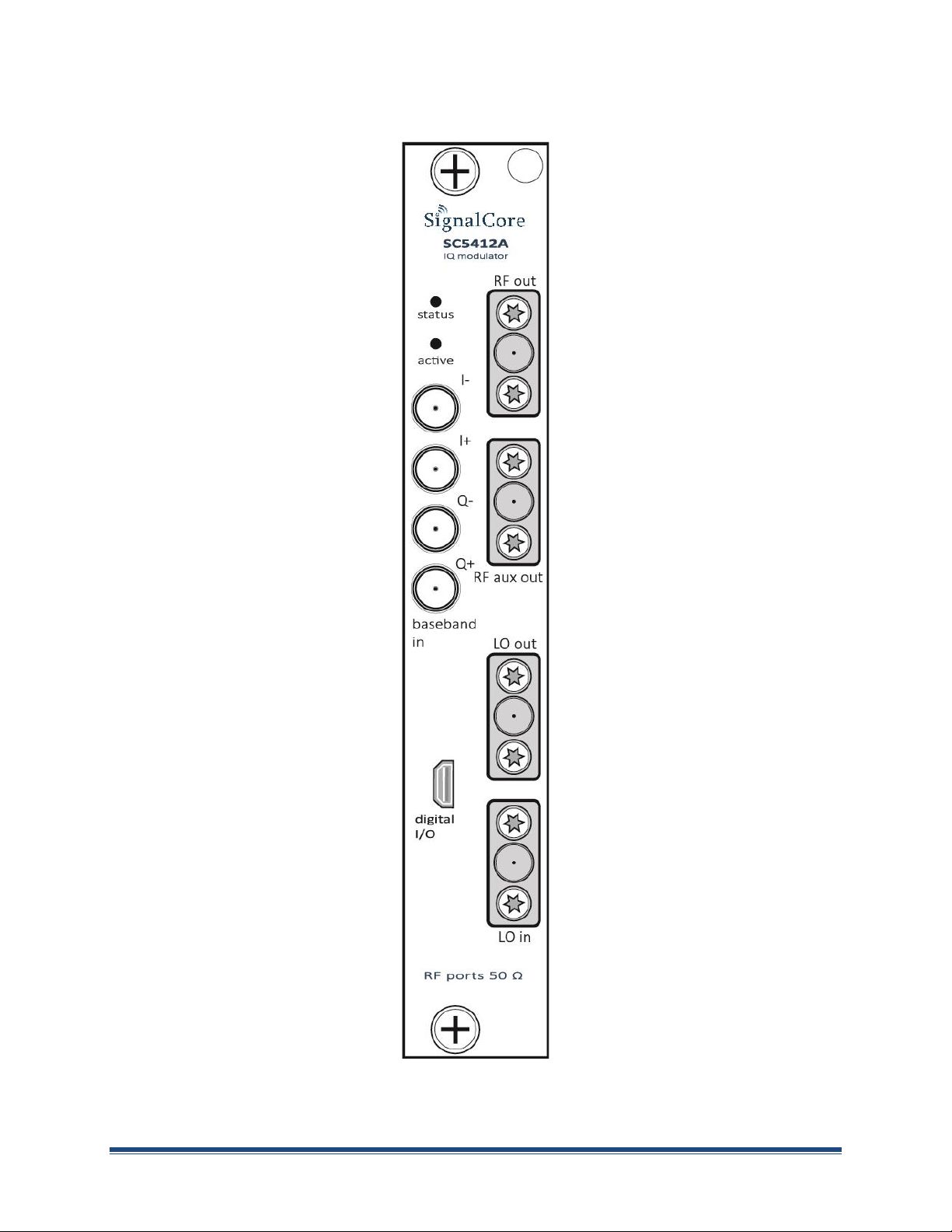
The SC5412A is a PXIe-based IQ modulator with all I/O connections and indicators located on the front
face of the module as shown below. Each location is discussed in further detail below.
Figure 1. PXIe chassis view of the SC5412A. Module is shown installed in slot 2.

SC5412A Operating & Programming Manual Rev 1.1.0 6
All RF signal connections (ports) on the SC5412A are SMA-type. Exercise caution when fastening cables
to the signal connections. Over-tightening any connection can cause permanent damage to the device.
The condition of your system‘s signal connections can significantly affect measurement
accuracy and repeatability. Improperly mated connections or dirty, damaged or worn
connectors can degrade measurement performance. Clean out any loose, dry debris from
connectors with clean, low-pressure air (available in spray cans from office supply stores).
If deeper cleaning is necessary, use lint-free swabs and isopropyl alcohol to gently clean
inside the connector barrel and the external threads. Do not mate connectors until the
alcohol has completely evaporated. Excess liquid alcohol trapped inside the connector may
take several days to fully evaporate and may degrade measurement performance until fully
evaporated.
Tighten all SMA connections to 5 in-lb max (56 N-cm max)
RF Signal Connections
LO OUT
This port outputs the tunable LO signal allowing phase-coherent daisy-
chaining of multiple IQ modulator modules. The connector is SMA female.
The nominal output impedance is 50 Ω.
RF OUT
This is the main RF signal output port ranging from 400 MHz to 6 GHz. The
connector is SMA female. The nominal input impedance is 50 Ω.
RF AUX OUT
This is the auxiliary RF signal output port ranging from 400 MHz to 6 GHz.
This port can be used as an alternate path for system-level calibration. The
connector is SMA female. The nominal input impedance is 50 Ω.
LO IN
This port accepts a tunable LO signal from an external source to drive the
modulator. The connector is SMA female. This port is AC-coupled with a
nominal input impedance of 50 Ω. Maximum input power is +10 dBm.
!
!
1

SC5412A Operating & Programming Manual Rev 1.1.0 7
Baseband Connections
The SC5412A has four baseband input ports, comprised of differential in-phase (I+ and I-) and
differential quadrature (Q+ and Q-) inputs. Nominal differential input impedance is 100 Ω. The
modulator can also be configured for single-ended or differential IF input. When configured for single-
ended operation, it is recommended to terminate the other half of the differential pair using a 50 Ω
terminator. All baseband connectors are MCX female.
Indicator LED
The SC5412A provides visual indication of important modes. There is one LED indicator on the unit. Its
behavior under different operating conditions is shown in Table 1.
Table 1. LED indicator states.
LED
Color
Definition
STATUS
Green
“Power good” and device is ready.
STATUS
Off
Power fault. Contact SignalCore.
ACTIVE
Green/Off
Device is open (green) /closed (off). This indicator is also
user programmable (see register map).
3
2

SC5412A Operating & Programming Manual Rev 1.1.0 8
SC5 4 1 2 A TH E O R Y O F OP E R A T I O N
Overview
The SC5412A is a single-stage, direct conversion Inphase-Quadrature (IQ) modulator. The modulator
operates in the 400 MHz to 6 GHz RF range with a typical 3 dB IQ IF bandwidth of 320 MHz. IF signals are
conditioned by input differential drivers prior to the IQ mixers. These differential drivers adjust the DC
level and minimize the DC offset effects on the modulated RF signal. The RF output stage has adjustable
gain to allow the user to adjust the signal levels, and to also to optimize for signal dynamic range. The
SC5412A has the necessary RF amplifiers, attenuators and IF amplifiers to give the user optimal control
of the device over the entire frequency range. Figure 3 shows a simplified block diagram of the SC5412A,
showing only the signal conditioning components critical for the following discussion. The following
sections provide more in-depth discussion on how to optimize the converter for linearity and signal-
noise dynamic range. Power supply generation and regulation, and digital control functions are not
covered. Should the user require more information than what is provided in this manual, please contact
SignalCore.
IF Input Section
The IF inputs are typically driven differentially, however they may also be driven single-ended. The IF
input is DC coupled with a differential impedance of 100 .Singled-ended operation is recommended
for AC-coupled operation due to the fact that DC-coupled single-ended operation may cause large DC
offsets at the input driver amplifier that the DC offset compensation may not be about to overcome. A
large DC offset will lead to high LO leakage, so unless the DC points of the differential inputs are bias the
same, AC coupling is recommended for single-end operation. For differential DC-coupled input it is
recommended to drive the common mode input voltage between 1.5 V to 2.5 V for best linearity
performance. See Figure 2 for details of the input section.
From Figure 3, the IF signals are first filtered by a 160 MHz filter, and then passed to the input
differential drivers before being driven into the IQ mixers. The DC characteristics of the output of each
differential driver are controlled by two 14 bit DACs. One DAC controls the driver common output
voltage, while a separate DAC controls the DC offset of the differential output pair. The common output
voltage has a range from 0V to 2.5V (DAC code 0 to 16383), and a differential voltage range of -50 mV to
+50 mV (DAC code 0 to 16383, mid code is 0V). The common output voltage controls the bias to the
mixer inputs, which affects the mixer linearity. The user may need to adjust this voltage to optimize
linearity (IP3 and harmonics), which is dependent on IF input power level and the operating frequency. A
typical bias voltage may range between 1 V and 3 V.
DC offset to the differential modulating mixer is controlled using the DC offset DAC. This DAC provides
approximately -50 mV to +50 mV of differential voltage adjustment. Adjusting the DAC offset on both
the I and Q channels can minimize the LO leakage at the RF output. This is commonly known as “nulling”
out the LO. The process typically involves a few adjustment steps alternating between the I-Channel DAC
and the Q-Channel DAC until an optimal level of LO suppression is achieved. However, nulling of the LO
is typically only effective over a small amplitude, frequency, and temperature range. Once the operating

SC5412A Operating & Programming Manual Rev 1.1.0 9
condition changes significantly, nulling may need to be performed again. For example, if the LO is nulled
at 25 OC, then it will most likely need to be nulled again at 45 OC although the frequency and input
amplitude is held relatively constant. Digital data must be corrected to compensate for the modulator IQ
amplitude and phase imbalances in addition to nulling out the LO leakage for best application results.
The IQ core, comprising two mixers driven at LO quadrature signals, should not be driven too hard with
IF signals because the resulting IMD3 of the RF signal may be too high. It is recommended to use an IF
level of 0.5 V peak-to-peak differential or less to lower the IMD3. However if the IF is too low, the RF
signal-to-noise ratio may suffer. Subsequently, the user must look at the RF result to determine the
optimal IF input level.
Figure 2. IF input section.
RF Output Section
The output section comprises adjustable digital step attenuators (DSA), RF amplifiers (one is selectable),
and a bank of low pass filters to suppress RF harmonics. These are used to condition the RF signal
generated in the IQ core component. The RF signal has its best performance exiting the IQ core;
therefore it is important to select a suitable RF gain to minimize further degradation of the signal. A
general rule is to apply more attenuation earlier in the RF path (close to the IQ core) to improve
linearity, and more gain to improve signal-to-noise performance. Generally, for RF frequencies less than
3 GHz, to vary signal levels greater than -20dBm the attenuators RF ATTEN#1, and RF ATTEN#2 should
be used as controls. To lower signal levels below -20 dBm, ATTEN#3 and ATTEN#4 should then be used.
Although all attenuators in the path have 30 dB of adjustment with 1 dB steps, it is not always
recommended to maximize the full range of an attenuator before moving to the next one in the path. As
an example, attenuation of ATTEN#1 should rarely be more than 10 dB because any further attenuation
will degrade the signal-to-noise ratio at a faster rate than the improvement of IMD3. If any further IMD3
improvement is needed, ATTEN#2 or ATTEN#3 should be used to create the desired attenuation.
ATTEN#4 should be fully utilized first to generate signals lower than -30 dBm.
The selectable RF amplifier is used to improve the overall gain of the device for frequencies in the 5 GHz
to 6 GHz range, as the RF loss in the RF path become more significant at these higher frequencies. The
gain flatness roll-off over the entire operating band is typically 15-16 dB. The RF amplifier has 14 dB of
gain. If the overall gain is too excessive at the desired operating frequency, ATTEN#2 should be used to
readjust the gain to the required level.
Vocm
100
100
100
100
Vocm
DAC
200
25
25
100Input Diff
Impedance
IQ MOD
I
25to 100
LPF 160 MHz LPF
Differential
Driver

SC5412A Operating & Programming Manual Rev 1.1.0 10
90
0
RF Amp
#3
RF Amp
(selectable)
9 Selectable
RF Filters
9 Selectable
LO Filters
LO Amp
#2
LO Amp
#1
RF Atten
#1
RF Atten
#4 RF Atten
#3 RF Atten
#2
Vocm /
Linear
Adjust
DAC
DC
Offset
DAC
IQ MOD
I
2.5V
Ref
i+ (in)
i- (in)
5V
Ref
Vocm
Vocm
Diff
Drive
Amp
RF Amp
#2
RF
RF
Aux
LO
LO
Aux
IF (I)
IF (Q)
Figure 3. Simplified SC5412A block diagram.

SC5412A Operating & Programming Manual Rev 1.1.0 11
There are nine low pass filters in the RF filter bank. These filters are automatically selected when the
user enters the operating frequency. These filters can also be selected manually should the user choose
to do so. As with all filters, there is generally an amplitude roll-off as the frequency nears its 3 dB cutoff
point so it is important to understand that frequencies near the cutoff point may experience a slightly
faster roll-off of their IF bandwidth. A typical 1 dB IQ IF bandwidth is about 160 MHz. The user may want
to choose a higher frequency filter if this becomes a problem. See the section “Setting the SC5412A:
Writing to Configuration Registers” for more details. The filters in both the RF and LO filter banks are
identical and are listed below.
Filter Number
1 dB Cutoff Frequency
0
400 MHz
1
500 MHz
2
650 MHz
3
1000 MHz
4
1400 MHz
5
2000 MHz
6
2825 MHz
7
3800 MHz
8
6000 MHz
LO Input Section
The SC5412A requires an external RF signal as its “Local Oscillator” (LO) for the frequency conversion
process. The external RF signal must be connected to the “LO in” port. The typical required input level is
-3 dBm to 3 dBm. These levels are required to sufficiently drive the IQ modulator for good linearity
performance and conversion loss. The LO signal is conditioned through a bank of low-pass filters to
reduce the signal harmonics. Reducing the harmonics produces a “purer” signal tone, improving the
duty cycle of the LO as it drives the mixers of the modulator. Additionally, the LO signal can be passed
out of the device via the “LO out” port. This output can be used as the input LO source for another
modulator, for example. Driving multiple modulators (or demodulators when working with SignalCore’s
SC5312A) with the same derived LO signal optimizes phase coherency between them. When this port is
not in use, it is highly recommended to terminate it into a 50 load.

SC5412A Operating & Programming Manual Rev 1.1.0 12
SC5 4 1 2 A PR O G R A M M I N G IN T E R F A C E
Device Drivers
The SC5412A is programmed by writing to its set of configuration registers, and its data is read back
through its set of query registers. The user may program directly at register level or through the API
library functions provided. These API library functions are wrapper functions of the registers that
simplify the task of configuring the register bytes. The register specifics are covered in the next section.
Writing to and reading from the device at the register level through the API involves calls to the
sc5412a_RegWrite and sc5412a_RegRead functions respectively.
The SC5412A is programmed by writing to its set of configuration registers, and its status read back
through its set of query registers. The user may choose to program directly at register level or through
the API library functions provided. These API library functions are wrapper functions of the registers that
simplify the task of configuring of the register bytes. The register specifics are covered in the next
section. Writing to and reading from the device at the register level through the API involves calls to the
sc5412a_RegWrite and sc5412a_RegRead functions respectively.
For Microsoft WindowsTM operating systems, The SC5412A API is provided as a dynamic linked library,
sc5412a.dll. This API uses NI-VISATM to communicate with the device. Inclusion of the NI-VISA driver is
required for code development in programming languages such C, C++, or LabVIEWTM. For LabVIEWTM
support, an additional LabVIEW API, sc5412a.llb, is also provided. The functions in the LabVIEW API are
primarily LabVIEW VI wrappers to the standard API functions. NI-VISATM is available from National
Instruments Corporation (www.ni.com).
For other operating systems or VISA implementations such as Agilent VISA, users will need to access the
device through their own proprietary PXIe driver. The VISA-based driver code is available to our
customers by request. This code can be compiled with Agilent VISA with minimal or no code change.
Should the user require assistance in writing an appropriate API other than that provided, please contact
SignalCore for additional example code and hardware details.
Using the Application Programming Interface (API)
The SC5412A API library functions make it easy for the user to communicate with the device. Using the
API removes the need to understand register-level details - their configuration, address, data format,
etc., and the additional layer between the PXIe bridge and the onboard microcontroller that must be
configured prior to writing the device registers. Using the API, commands to control the device are
greatly simplified. For example, to obtain the device temperature, the user simply calls the function
sc5412a_GetDeviceTemperature, or calls sc5412a_SetFrequency to tune the frequency. The software
API is covered in detail in the “Software API Library Functions” section.

SC5412A Operating & Programming Manual Rev 1.1.0 13
SE T T I N G T H E SC5 4 1 2 A : WR I T I N G T O
CO N F I G U R A T I O N RE G I S T E R S
Configuration Registers
The users may write the configuration registers (write only) directly by calling the sc5412a_RegWrite
function. The syntax for this function is sc5412a_RegWrite(deviceHandle, registerCommand,
instructWord). The instructWord takes a 64 bit-word. However, it will only send the required number of
bytes to the device. Table 2 summarizes the register addresses (commands) and the effective bytes of
command data.
Table 2. Configuration registers.
Register (Address)
Reg
Code
Serial
Range
MSB
Bit 7
MSB
Bit 6
MSB
Bit 5
MSB
Bit 4
MSB
Bit 3
MSB
Bit 2
MSB Bit
1
MSB Bit
0
INITIALIZE
0x01
[7:0]
Mode
SET_SYSTEM_ACTIVE
0x02
[7:0]
Enable
SYS LED
RF_FREQUENCY
0x10
[7:0]
MHz Frequency Word [7:0]
[15:8]
MHz Frequency Word [15:8]
[23:16]
MHz Frequency Word [23:16]
[31:24]
MHz Frequency Word [31:24]
[39:32]
MHz Frequency Word [39:32]
RF_AMPLIFIER
0x12
[7:0]
Amplifier
Mode
RF_ATTENUATION
0x13
[7:0]
Attenuation
[15:8]
Attenuator #
RF_PATH
0x14
[7:0]
Path
RF_FILTER_SELECT
0x15
[7:0]
Filter [3:0]
LO_FILTER_SELECT
0x16
[7:0]
Filter [3:0]
LO_OUT_ENABLE
0x17
[7:0]
Enable
LO Out
DC_OFFSET_DAC
0x1A
[7:0]
DAC value [7:0]
[15:8]
DAC value [13:8]
[23:16]
Channel
LINEARITY_DAC
0x1B
[7:0]
DAC value [7:0]
[15:8]
DAC value [13:8]
[23:16]
Channel
STORE_STARTUP_STATE
0x1D
[7:0]
USER_EEPROM_WRITE
0x1F
[7:0]
Address [7:0]
[15:8]
Address [15:8]
[23:16]
Byte[7:0]

SC5412A Operating & Programming Manual Rev 1.1.0 14
Initializing the Device
INITIALIZE (0x01) - Writing 0x00 to this register will reset the device to the default power-on state.
Writing 0x01 will reset the device but leave it in the current state. The user has the ability to define the
default startup state by writing to the STORE_STARTUP_STATE (0x1D) register, described later in this
section.
Setting the System Active LED
SET_SYSTEM_ACTIVE (0x02) - This register simply turns on the front panel “active” LED with a write of
0x01, or turns off the LED with a write of 0x00. This register is generally written when the device driver
opens or closes the device.
Setting the RF Frequency
RF_FREQUENCY (0x10) - This register provides the device frequency information to set up the filters
appropriately. Data is sent as a 40 bit word with the LSB in Hz.
Setting RF Input RF Amplifiers
RF_AMPLIFIER (0x12) - This register enables or disables the RF amplifiers. Setting bit 0 low (0) disables
RF amplifier. Setting bit 0 high (1) enables RF amplifier.
Setting the RF Attenuation
RF_ATTENUATION (0x13) –Each of the attenuators is a 5 bit digital step attenuator with 1 dB per LSB.
Data is sent in 2 bytes; byte1 and bits [1:0] specifies the attenuator to program, and byte0 and bit [4:0]
specifies the attenuation value.
Setting the RF Path
RF_PATH (0x14) –Setting bit 0 low selects the main RF input path, while high will select the RF auxiliary
path.
Selecting the RF Filter
RF_FILTER_SELECT (0x15) –There are 9 RF filters to select from to improve RF input second harmonic
suppression. Bits [3:0] are used.
Selecting the LO Filter
LO_FILTER_SELECT (0x16) –There are 9 RF filters to select from to improve LO input second harmonic
suppression. Bits [3:0] are used.

SC5412A Operating & Programming Manual Rev 1.1.0 15
Enabling LO Output
LO_OUT_ENABLE (0x17) –Setting bit 0 high enables the LO signal to be ported out the LO output
connector. Note there is always a leakage out of this port and the levels could be as high as -30 dBm. It is
recommended to terminate this port into a 50 load if it is not used.
Removing DC Offset in Differential Amplifiers
DC_OFFSET_DAC (0x1A) –The DC offsets at the input of the modulator causes LO leakage. Adjustments
to both the I & Q channel differential DC offsets can minimize the LO leakage. Varying the DAC value
from 0 to 16383 can correct up to approximately of DC offset error. This correction resolution is
less than 0.010 mV per LSB. An approximation of the DAC value-to-offset voltage is given below.
Setting the Output Linearity of the IQ Modulator
LINEARITY_DAC (0x19) –This DAC controls the bias point of the IQ modulator. A typical value for the
bias point is 1.2V, however adjustments are needed to improve linearity at different operating
frequency and input IF power levels. Typically, the DAC is set around 1.2 V using the following equation:
Storing the Startup State
STORE_STARTUP_STATE (0x1D) –Writing to this register will save the current device state as the new
default power on (startup) state. All data written to this register will be ignored as only the write
command is needed to initiate the save.
Writing to the User EEPROM
USER_EEPROM_WRITE (0x1B) - There is an onboard 32 kilobyte EEPROM for the user to store data.
User data is sent one byte at a time and is contained in the last (least significant) byte of the three bytes
of data written to the register. The other two bytes contain the write address in the EEPROM. For
example, to write user data 0x22 into address 0x1F00 requires writing 0x1F0022 to this register.

SC5412A Operating & Programming Manual Rev 1.1.0 16
QU E R Y I N G T H E SC5 4 1 2 A : WR I T I N G T O
RE Q U E S T RE G I S T E R S
The registers to read data back from the device (such as device status) are accessed through the
sc5412a_RegRead function. The function and parameter format for this command is
sc5412a_RegRead(deviceHandle, registerCommand, instructWord,*dataOut). Any instructions in
addition to the register call are placed into “instructWord”, and data obtained from the device is
returned via the pointer value dataOut. The set of request registers are shown in Table 3.
Table 3. Query registers.
Register Name
Register
Address (Hex)
Serial
Range
Bit 7
Bit 6
Bit 5
Bit 4
Bit 3
Bit 2
Bit 1
Bit 0
GET_TEMPERATURE
0x20
[7:0]
Open
Open
Open
Open
Open
Open
Open
Open
GET_DEVICE_STATUS
0x21
[7:0]
Open
Open
Open
Open
Open
Open
Open
Open
USER EEPROM_READ
0x23
[7:0]
EEPROM Address [7:0]
[15:8]
EEPROM Address [15:8]
CAL_EEPROM_READ
0x24
[7:0]
EEPROM Address [7:0]
[15:8]
EEPROM Address [15:8]
Reading the Device Temperature
GET_TEMPERATURE (0x17) - Data returned by this register needs to be processed to correctly represent
data in temperature units of degrees Celsius. Data is returned in the first 14 bits [13:0]. Bit [13] is the
polarity bit indicating whether it is positive (0x0) or negative (0x1). For an ENDPOINT_IN transfer, data is
returned in 2 bytes with the MSB first. The temperature value represented in the raw data is contained
in the next 13 bits [12:0]. To obtain the temperature ADC code, the raw data should be masked (bitwise
AND’ed) with 0x1FFF, and the polarity should be masked with 0x2000. The conversion from 12 bit ADC
code to an actual temperature reading in degrees Celsius is shown below:
Positive Temperature (bit 13 is 0)
=
ADC code / 32
Negative Temperature (bit 13 is 1)
=
(ADC code –8192) / 32
It is not recommended to read the temperature too frequently, especially once the temperature of the
SC5412A has stabilized. The temperature sensor is a serial device located inside the RF module.
Therefore, like any other serial device, reading the temperature sensor requires a sending serial clock
and data commands from the processor. The process of sending clock pulses on the serial transfer line
may cause unwanted spurs on the RF signal as the serial clock could potentially modulate the externally-
supplied LO signal within the device.
Reading the Device Status
GET_DEVICE_STATUS (0x21) - This register, summarized in Table 4, returns the device status
information such as phase lock status of the PLL, current reference settings, etc. Data is contained in the
first three bytes.

SC5412A Operating & Programming Manual Rev 1.1.0 17
Table 4. Description of the status data bits.
Bit
Description
[4]
RF AMP#1 enable
[3]
RF AMP#2 enable
[2]
RF path selection
[1]
LO output enable
[0]
Device accessed
Reading the User EEPROM
USER_EEPROM_READ (0x23) - Once data has been written to the user EEPROM, it can be retrieved by
calling this register and using the process outlined in the next section for reading calibration data. The
maximum address for this EEPROM is 0x7FFF. A single byte is returned.
Reading the Calibration EEPROM
CAL_EEPROM_READ (0x24) - Reading a single byte from an address in the device EEPROM is performed
by writing this register with the address for the instructWord. The data is returned as a byte. The CAL
EEPROM maximum address is also 0x7FFF. Reading above this address will cause the device to retrieve
data from the lower addresses. For example, addressing 0x8000 will return data stored in address
location 0x0000. The calibration EEPROM map is shown in Table 5.
All calibration data, whether floats, unsigned 8-bit, unsigned 16-bit or unsigned 32-bit integers, are
stored as flattened unsigned byte representation. A float is flattened to 4 unsigned bytes, so once it is
read back it needs to be un-flattened back to its original type. Unsigned values containing more than a
single byte are converted (un-flattened) simply by concatenation of the bytes through bit-shifting.
Converting to floating point representation is slightly more involved. First, convert the 4 bytes into an
unsigned 32-bit integer value, and then (in C/C++) type-cast a float pointer to the address of the value.
In C/C++, the code would be float Y = *(float *)&X, where X has been converted earlier to an unsigned
integer. An example written in C code would look something like the following:
byte_value[4]; // read in earlier
unsigned int uint32_value;
float float32_value;
int count = 0;
while (count < 4) {
uint32_value = unit32_value | (byte_value[count] <<
(count*8));
count++;
}
float32_value = *(float *)&uint32_value;
Table of contents


