Silicon Laboratories SI4421 User manual

Si4421
PIN ASSIGNMENT
This document refers to Si4421-IC rev A1.
See www.silabs.com/integration for any applicable errata.
See back page for ordering information.
Si4421 Universal ISM Band
FSK Transceiver
DESCRIPTION
Silicon Labs’ Si4421 is a single chip, low power, multi-channel FSK
t
ransceiver designed for use in applications requiring FCC or ETSI
conformance for unlicensed use in the 433, 868 and 915 MHz bands.
The Si4421 transceiver is a part of Silicon Labs’ EZRadioTM
product
line, which produces a flexible, low cost, and highly integrated solution
t
hat does not require production alignments. The chip is a complete
analog RF and baseband transceiver including a multi-band PLL
synthesizer with PA, LNA, I/Q down converter mixers, baseband filters
and amplifiers, and an I/Q demodulator. All required RF functions are
integrated. Only an external crystal and bypass filtering are needed for
operation.
The Si4421 features a completely integrated PLL for easy RF design,
and its rapid settling time allows for fast frequency-hopping, bypassin
g
multipath fading and interference to achieve robust wireless links. The
PLL’s high resolution allows the usage of multiple channels in any o
f
t
he bands. The receiver baseband bandwidth (BW) is programmable to
accommodate various deviation, data rate and crystal tolerance
requirements. The transceiver employs the Zero-IF approach with I/Q
demodulation. Consequently, no external componen
t
s (except crystal
and decoupling) are needed in most applications.
The Si4421 dramatically reduces the load on the microcontroller with
t
he integrated digital data processing features: data filtering, clock
recovery, data pattern recognition, integrated FIFO and TX data
register. The automatic frequency control (AFC) feature allows the use
of a low accuracy (low cost) crystal. To minimize the system cost, the
Si4421 can provide a clock signal for the microcontroller, avoiding the
need for two crystals.
For low power applications, the Si4421 supports low duty cycle
operation based on the internal wake-up timer.
FUNCTIONAL BLOCK DIAGRAM
1
Si4421-DS rev 2.4r 0708 www.silabs.com
RF Parts Data processing units
Low Power parts
AMP OC
AMP OC
LNA
MIX I
Q
MIX
Data Filt
CLK Rec data
clk
BB Amp/Filt./Limiter
DQDCOMP
RSSI AFC
Self cal.
PLL & I/Q VCO
with cal.
ControllerXosc LBD
WTM
with cal.
CLK div Bias
13
RF1
RF2 12
7
6
DCLK /
CFIL /
FFIT /
FSK /
DATA /
nFFS
FIFO
8 9
CLK XTL /
REF
10
15
nINT /
VDI
ARSSI
23 4 511
SCK nSEL SDO nIRQ
14
1
VSS VDD
SDI
16
nRES
PA
I/Q
DEMOD
FEATURES
Fully integrated (low BOM, easy design-in)
No alignment required in production
Fast-settling, programmable, high-resolution PLL synthesizer
Fast frequency-hopping capability
High bit rate (up to 115.2 kbps in digital mode and 256 kbps
in analog mode)
Direct differential antenna input/output
Integrated power amplifier
Programmable TX frequency deviation (15 to 240 kHz)
Programmable RX baseband bandwidth (67 to 400 kHz)
Analog and digital RSSI outputs
Automatic frequency control (AFC)
Data quality detection (DQD)
Internal data filtering and clock recovery
RX synchron pattern recognition
SPI compatible serial control interface
Clock and reset signals for microcontroller
16-bit RX Data FIFO
Two 8-bit TX data registers
Low power duty cycle mode
Standard 10 MHz crystal reference with on-chip tuning
Wake-up timer
2.2 to 3.8 V supply voltage
Low power consumption
Low standby current (0.3 A)
Compact 16 pin TSSOP package
Supports very short packets (down to 3 bytes)
Excellent temperature stability of the RF parameters
Good adjacent channel rejection/blocking
TYPICAL APPLICATIONS
Home security and alarm
Remote control, keyless entry
Wireless keyboard/mouse and other PC peripherals
Toy controls
Remote keyless entry
Tire pressure monitoring
Telemetry
Personal/patient data logging
Remote automatic meter reading

Si4421
2
DETAILED FEATURE-LEVEL DESCRIPTION
The Si4421 FSK transceiver is designed to cover the unlicensed
frequency bands at 433, 868 and 915 MHz. The device
facilitates compliance with FCC and ETSI requirements.
The receiver block employs the Zero-IF approach with I/Q
demodulation, allowing the use of a minimal number of external
components in a typical application. The Si4421 incorporates a
fully integrated multi-band PLL synthesizer, PA with antenna
tuning, an LNA with switchable gain, I/Q down converter mixers,
baseband filters and amplifiers, and an I/Q demodulator
followed by a data filter.
PLL
The programmable PLL synthesizer determines the operating
frequency, while preserving accuracy based on the on-chip crystal-
controlled reference oscillator. The PLL’s high resolution allows the
usage of multiple channels in any of the bands.
RF Power Amplifier (PA)
The power amplifier has an open-collector differential output and
can directly drive different PCB antennas with a programmable
output power level. An automatic antenna tuning circuit is built in
to avoid costly trimming procedures and the so-called “hand
effect”.
LNA
The LNA has approximately 250 Ohm input impedance, which
functions well with the proposed antennas (see: Application
Notes available from www.silabs.com/integration)
If the RF input of the chip is connected to 50 Ohm devices, an
external matching circuit is required to provide the correct
matching and to minimize the noise figure of the receiver.
The LNA gain can be selected in four steps (between 0 and
-20dB relative to the highest gain) according to RF signal
strength. It can be useful in an environment with strong
interferers.
Baseband Filters
The receiver bandwidth is selectable by programming the
bandwidth (BW) of the baseband filters. This allows setting up
the receiver according to the characteristics of the signal to be
received.
An appropriate bandwidth can be chosen to accommodate
various FSK deviation, data rate and crystal tolerance
requirements. The filter structure is 7th order Butterworth low-
pass with 40 dB suppression at 2 · BW frequency. Offset
cancellation is done by using a high-pass filter with a cut-off
frequency below 7 kHz.
Full Baseband Amplifier Transfer Function
BW=67kHz
Data Filtering and Clock Recovery
Output data filtering can be completed by an external capacitor
or by using digital filtering according to the final application.
Analog operation: The filter is an RC type low-pass filter followed
by a Schmitt-trigger (St). The resistor (10 kOhm) and the St are
integrated on the chip. An (external) capacitor can be chosen
according to the actual bit rate. In this mode, the receiver can
handle up to 256 kbps data rate. The FIFO cannot be used in this
mode and clock is not provided for the demodulated data.
Digital operation: A digital filter is used with a clock frequency at
29 times the bit rate. In this mode, there is a clock recovery
circuit (CR), which can provide synchronized clock to the data.
Using this clock the received data can fill a FIFO. The CR has
three operation modes: fast, slow, and automatic. In slow mode,
its noise immunity is very high, but it has slower settling time and
requires more accurate data timing than in fast mode. In
automatic mode, the CR automatically changes between fast and
slow mode. The CR starts in fast mode, then after locking, it
automatically switches to slow mode
(Only the digital data filter and the clock recovery use the bit rate
clock. For analog operation, there is no need for setting the
correct bit rate.)

Si4421
3
Data Validity Blocks
RSSI
A digital RSSI output is provided to monitor the input signal level.
It goes high if the received signal strength exceeds a given
preprogrammed level. An analog RSSI signal is also available.
The RSSI settling time depends on the external filter capacitor.
Pin 15 is used as analog RSSI output. The digital RSSI can be
monitored by reading the status register.
Typical Analog ARSSI Voltage vs. RF Input Power
DQD
The operation of the Data Quality Detector is based on counting
the spikes on the unfiltered received data. High output signal
indicates an operating FSK transmitter within baseband filter
bandwidth from the local oscillator. DQD threshold parameter
can be set by using the Data Filter Command (page 19).
AFC
By using an integrated Automatic Frequency Control (AFC)
feature, the receiver can minimize the TX/RX offset in discrete
steps, allowing the use of:
Narrower receiver bandwidth (i.e. increased
sensitivity)
Higher data rate
Inexpensive crystals
Crystal Oscillator
The Si4421 has a single-pin crystal oscillator circuit, which
provides a 10 MHz reference signal for the PLL. To reduce
external parts and simplify design, the crystal load capacitor is
internal and programmable. Guidelines for selecting the
appropriate crystal can be found later in this datasheet.
The transceiver can supply a clock signal for the microcontroller;
so accurate timing is possible without the need for a second
crystal.
When the microcontroller turns the crystal oscillator off by
clearing the appropriate bit using the Power Management
Command (page 15), the chip provides a fixed number (192) of
further clock pulses (“clock tail”) for the microcontroller to let it
go to idle or sleep mode. If this clock output is not used, it is
suggested to turn the output buffer off by the Power
Management Command (page 15).
Low Battery Voltage Detector
The low battery detector circuit monitors the supply voltage and
generates an interrupt if it falls below a programmable threshold
level. The detector circuit has 50 mV hysteresis.
Wake-Up Timer
The wake-up timer has very low current consumption (1.5 µA
typical) and can be programmed from 1 ms to several days with
an accuracy of ±10%.
The wake-up timer calibrates itself to the crystal oscillator at
every startup. For proper calibration of the wake-up timer the
crystal oscillator must be running before the wake-up timer is
enabled. The calibration process takes approximately 0.5ms.
For the crystal start up time (tsx), see page 11.
Event Handling
In order to minimize current consumption, the transceiver
supports different power saving modes. Active mode can be
initiated by several wake-up events (negative logical pulse on
nINT input, wake-up timer timeout, low supply voltage detection,
on-chip FIFO filled up or receiving a request through the serial
interface).
If any wake-up event occurs, the wake-up logic generates an
interrupt signal, which can be used to wake up the
microcontroller, effectively reducing the period the
microcontroller has to be active. The source of the interrupt can
be read out from the transceiver by the microcontroller through
the SDO pin.
Interface and Controller
An SPI compatible serial interface lets the user select the
frequency band, center frequency of the synthesizer, and the
bandwidth of the baseband signal path. Division ratio for the
microcontroller clock, wake-up timer period, and low supply
voltage detector threshold are also programmable. Any of these
auxiliary functions can be disabled when not needed. All
parameters are set to default after power-on; the programmed
values are retained during sleep mode. The interface supports
the read-out of a status register, providing detailed information
about the status of the transceiver and the received data.
The transmitter block is equipped with two 8-bit wide TX data
registers. It is possible to write 8 bits into the register in burst
mode and the internal bit rate generator transmits the bits out
with the predefined rate. For further details, see the TX Register
Buffered Data Transmission section (page 28).
It is also possible to store the received data bits into a FIFO
register and read them out in a buffered mode.

Si4421
PACKAGE PIN DEFINITIONS
Pin type key: D=digital, A=analog, S=supply, I=input, O=output, IO=input/output
Pin Name Type Function
1 SDI DI Data input of the serial control interface
2 SCK DI Clock input of the serial control interface
3 nSEL DI Chip select input of the serial control interface (active low)
4 SDO DO Serial data output with bus hold
5 nIRQ DO Interrupt request output (active low)
FSK DI Transmit FSK data input (internal pull up resistor 133 k)
DATA DO Received data output (FIFO not used)
6
nFFS DI
FIFO select input (active low). In FIFO mode, when bit ef is set in Configuration Setting Command,
page 15 (internal pull up resistor 133 k)
DLCK DO Received data clock output (Digital filter used, FIFO not used)
CFIL AIO External data filter capacitor connection (Analog filter used)
7
FFIT DO FIFO interrupt (active high). In FIFO mode, when bit ef is set in Configuration Setting Command
8 CLK DO Microcontroller clock output
XTL AIO Crystal connection (the other terminal of crystal to VSS) or external reference input
9
REF AIO External reference input. Use 33 pF series coupling capacitor
10 nRES DIO Open drain reset output with internal pull-up and input buffer (active low)
11 VSS S Ground reference voltage
12 RF2 AIO RF differential signal input/output
13 RF1 AIO RF differential signal input/output
14 VDD S Positive supply voltage
15 ARSSI AO Analog RSSI output
nINT DI Interrupt input (active low)
16
VDI DO Valid data indicator output
Note: The actual mode of the multipurpose pins (pin 6 and 7) is determined by the TX/RX data I/O settings of the transceiver.
4

Si4421
5
Internal Pin Connections
Pin Name Internal connection
1 SDI
2 SCK
3 nSEL
PAD
1.5k
VSS
VDD
4 SDO
5 nIRQ
FSK
DATA
6
nFFS
DLCK
CFIL
7
FFIT
8 CLK PAD
10
VSS
VDD
XTL
9
REF
Pin Name Internal connection
10 nRES
11 VSS
12 RF2
13 RF1
14 VDD
15 ARSSI
nINT
16
VDI

Si4421
PIN6 Logic Diagram (FSK / DATA / nFFS)
PIN10 Logic Diagram (nRES I/O)
* Note: These pins can be left floating.
6

Si4421
7
Typical Application
Typical application with FIFO usage
C3 C2
10n
X1
10MHz
C1
2.2u
Si4421
1
3
4
2
5
7
6
89
10
11
12
13
14
15
16
VDD
SCK
SDO
nIRQ
P4
P3
P1
P2
SDI
CLKin
nSEL
nFFS
FFIT
nRES
PCB
Antenna
P5
P6
P7
nRESin
C4
2.2n
P0
CLK
(optional)*
TP
(optional)
(optional)*
(optional)
(opt.)
(optional)
VDI
Note: * Connections needed only in time critical applications
Recommended supply decoupling capacitor values
C2 and C3 should be 0603 size ceramic capacitors to achieve the best supply decoupling.
Band [MHz] C1 C2 C3
433 2.2µF 10nF 220pF
868 2.2µF 10nF 47pF
915 2.2µF 10nF 33pF
Property C1 C2 C3
SMD size A 0603 0603
Dielectric Tantalum Ceramic Ceramic
Pin Function vs. Operation Mode
Mode Bit setting Function Pin 6 Pin 7
el = 0 Internal TX data register disabled TX data input
Transmit
el = 1 Internal TX data register enabled nFFS input
(TX data register can be accessed)
Not used
ef = 0 Receiver FIFO disabled RX data output RX data clock
output
Receive
ef = 1 Receiver FIFO disabled nFFS input
(RX data FIFO can be accessed) FFIT output
The el and ef bits can be found in the Configuration Setting Command on page 15. Bit el enables the internal TX data register.
Bit ef enables the FIFO mode.

Si4421
GENERAL DEVICE SPECIFICATIONS
All voltages are referenced to Vss , the potential on the ground reference pin VSS.
Absolute Maximum Ratings (non-operating)
Symbol Parameter Min Max Units
Vdd Positive supply voltage -0.5 6 V
Vin Voltage on any pin (except RF1 and RF2) -0.5 Vdd +0.5 V
Voc Voltage on open collector outputs (RF1, RF2) -0.5 Vdd +1.5 (Note 1) V
Iin Input current into any pin except VDD and VSS -25 25 mA
ESD Electrostatic discharge with human body model 1000 V
Tst Storage temperature -55 125 oC
Tld Lead temperature (soldering, max 10 s) 260 oC
Recommended Operating Range
Symbol Parameter Min Max Units
Vdd Positive supply voltage 2.2 3.8 V
Voc Voltage range on open collector outputs (RF1, RF2) Vdd -1.5 (Note 2) Vdd +1.5 V
Top Ambient operating temperature -40 85 oC
Note 1: The voltage on RF1 and RF2 pins can be higher than the actual Vdd but cannot exceed 7 V.
Note 2: The actual voltage on RF1 and RF2 pins can be lower than the current Vdd but never should go below 1.2 V.
8

Si4421
ELECTRICAL SPECIFICATION
Test Conditions: Top = 27 oC; Vdd = Voc = 3.3 V
DC Characteristics
Symbol Parameter Conditions/Notes Min Typ Max Units
433 MHz band 15
868 MHz band 16
Idd_TX_0 Supply current
(TX mode, Pout = 0 dBm)
915 MHz band 17
mA
433 MHz band 22 26
868 MHz band 23 27
Idd_TX_PMAX Supply current
(TX mode, Pout = Pmax)
915 MHz band 24 28
mA
433 MHz band 11 13
868 MHz band 12 14
Idd_RX Supply current (RX mode)
915 MHz band 13 15
mA
Ipd Standby current (Sleep mode) All blocks disabled 0.3 1 µA
Ilb Low battery voltage detector current
consumption 0.5 1.7 µA
Iwt Wake-up timer current consumption 1.5 3.5 µA
Ix Idle current Crystal oscillator on (Note 1) 0.6 1.2 mA
Vlb Low battery detect threshold Programmable in 0.1 V steps 2.25 3.75 V
Vlba Low battery detection accuracy ± 3 %
Vil Digital input low level voltage 0.3·Vdd V
Vih Digital input high level voltage 0.7·Vdd V
Iil Digital input current Vil = 0 V -1 1 µA
Iih Digital input current Vih = Vdd , Vdd = 3.8 V -1 1 µA
Vol Digital output low level Iol = 2 mA 0.4 V
Voh Digital output high level Ioh = -2 mA Vdd -0.4 V
Notes are on page 12.
9
Si4421
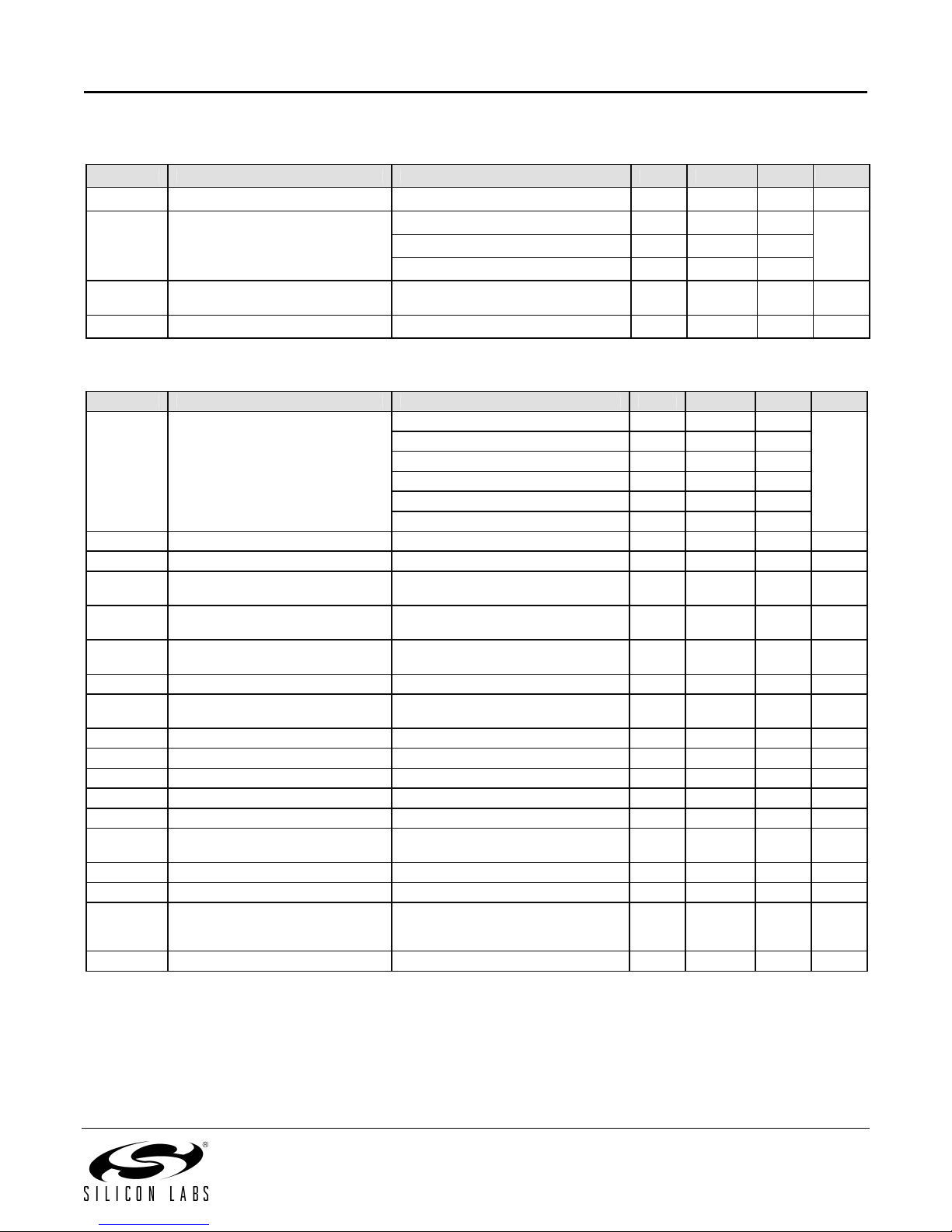
AC Characteristics (PLL parameters)
Symbol Parameter Conditions/Notes Min Typ Max Units
fref PLL reference frequency (Note 2) 9 10 11 MHz
433 MHz band, 2.5 kHz resolution 430.24 439.75
868 MHz band, 5.0 kHz resolution 860.48 879.51
foReceiver LO/Transmitter carrier
frequency
915 MHz band, 7.5 kHz resolution 900.72 929.27
MHz
tlock PLL lock time Frequency error < 1kHz
after 10 MHz step 30 µs
tstP PLL startup time (Note 10) With a running crystal oscillator 200 300 µs
AC Characteristics (Receiver)
Symbol Parameter Conditions/Notes Min Typ Max Units
mode 0 67
mode 1 134
mode 2 200
mode 3 270
mode 4 340
BW Receiver bandwidth
mode 5 400
kHz
BRRX FSK bit rate (Note 10) With internal digital filters 0.6 115.2 kbps
BRARX FSK bit rate (Note 10) With analog filter 256 kbps
Pmin Receiver Sensitivity BER 10-3, BW=67 kHz, BR=1.2 kbps,
868 MHz Band (Note 3) -110 dBm
AFCrange AFC locking range δfFSK: FSK deviation in the received
signal
0.8
·
δf
FSK
IIP3inh Input IP3 In band interferers in high bands
(868 MHz, 915 MHz) -21 dBm
IIP3outh Input IP3 Out of band interferers l f-fo l> 4 MHz -18 dBm
IIP3inl IIP3 (LNA –6 dB gain) In band interferers in low band (433
MHz) -15 dBm
IIP3outl IIP3 (LNA –6 dB gain) Out of band interferers l f-fo l> 4 MHz -12 dBm
Pmax Maximum input power LNA: high gain 0 dBm
Cin RF input capacitance 1 pF
RSaRSSI accuracy ± 6 dB
RSrRSSI range 46 dB
RSps RSSI power supply dependency When input signal level lower than -54
dBm and greater than -100 dBm +35 mV/V
CARSSI Filter capacitor for ARSSI 1 nF
RSstep RSSI programmable level steps 6 dB
RSresp DRSSI response time
Until the RSSI signal goes high after
the input signal exceeds the
preprogrammed limit CARRSI = 4.7 nF
500 µs
Psp_rx Receiver spurious emission -60 dBm
Notes are on page 12.
10

Si4421
AC Characteristics (Transmitter)
Symbol Parameter Conditions/Notes Min Typ Max Units
IOUT Open collector output DC current Programmable 0.5 6 mA
In 433 MHz band 7
Pmax_50
Max. output power delivered to 50
Ohm load over a suitable matching
network (Note 4) In 868 MHz / 915 MHz bands 5
dBm
In 433 MHz band with monopole antenna
with matching network (Note 4) 7
Pmax_ant Max. EIRP with suitable selected
PCB antenna (Note 6)
In 868 MHz / 915 MHz bands (Note 5) 7
dBm
Pout Typical output power Selectable in 2.5 dB steps (Note 7) Pmax-17.5 Pmax dBm
At max power 50 Ohm load (Note 4) -55
Psp Spurious emission
l f-fsp l> 1 MHz With PCB antenna (Note 5) -60
dBc
At max power 50 Ohm load (Note 4) -35
Pharm Harmonic suppression
With PCB antenna (Note 5) -42
dBc
In 433 MHz band 2 2.6 3.2
CoOutput capacitance (set by the
automatic antenna tuning circuit) In 868 MHz / 915 MHz bands 2.1 2.7 3.3
pF
In 433 MHz band 13 15 17
QoQuality factor of the output
capacitance In 868 MHz / 915 MHz bands 8 10 12
100 kHz from carrier, in 868 MHz band -80
Lout Output phase noise
1 MHz from carrier, in 868 MHz band -103
dBc/Hz
BRTX FSK bit rate Via internal TX data register 172 kbps
BRATX FSK bit rate TX data connected to the FSK input 256 kbps
dffsk FSK frequency deviation Programmable in 15 kHz steps 15 240 kHz
AC Characteristics (Turn-on/Turnaround timings)
Symbol Parameter Conditions/Notes Min Typ Max Units
tsx Crystal oscillator startup time
Default capacitance bank setting, crystal
ESR < 50 Ohm (Note 9). Crystal load
capacitance = 16 pF.
2 7 ms
Ttx_XTAL_ON Transmitter turn-on time Synthesizer off, crystal oscillator on with
10 MHz step 250 µs
Trx_XTAL_ON Receiver turn-on time Synthesizer off, crystal oscillator on with
10 MHz step 250 µs
Ttx_rx_SYNT_ON Transmitter – Receiver turnover time Synthesizer and crystal oscillator on
during TX/RX change with 10 MHz step 150 µs
Trx_tx_SYNT_ON Receiver – Transmitter turnover time Synthesizer and crystal oscillator on
during RX/TX change with 10 MHz step 150 µs
AC Characteristics (Others)
Symbol Parameter Conditions/Notes Min Typ Max Units
Cxl Crystal load capacitance,
see crystal selection guide
Programmable in 0.5 pF steps, tolerance
± 10% 8.5 16 pF
tPOR Internal POR timeout After Vdd has reached 90% of final value
(Note 8) 100 ms
tPBt Wake-up timer clock accuracy
Crystal oscillator must be enabled to
ensure proper calibration at the start up.
(Note 9)
± 10 %
CinD Digital input capacitance 2 pF
tr, tfDigital output rise/fall time 15 pF pure capacitive load 10 ns
Notes are on page 12.
11

Si4421
Note 1: Measured with disabled clock output buffer
Note 2: Not using a 10 MHz crystal is allowed but not recommended because all crystal referred timing and frequency parameters
will change accordingly
Note 3: See the BER diagrams in the measurement results section (page 37) for detailed information
Note 4: See reference design with 50 Ohm Matching Network (page 39) for details
Note 5: See reference design with Resonant PCB Antenna (BIFA) on page 41 for details
Note 6:Optimal antenna admittance/impedance:
Si4421 Yantenna [mS] Zantenna [Ohm] Lantenna [nH]
433 MHz 2 – j5.9 52 + j152 62
868 MHz 1.2 - j11.9 7.8 + j83 15.4
915 MHz 1.49 - j12.8 9 + j77 13.6
Note 7: Adjustable in 8 steps
Note 8: During the Power-On Reset period, commands are not accepted by the chip. In case of software reset (see Wake-Up Timer
Command, page 25) the reset timeout is 0.25ms typical.
Note 9: The crystal oscillator start up time strongly depends on the capacitance seen by the oscillator. Low capacitance and low
ESR crystal is recommended with low parasitic PCB layout design.
Note 10: By design
12

Si4421
CONTROL INTERFACE
Commands to the transmitter are sent serially. Data bits on pin SDI are shifted into the device upon the rising edge of the clock on
pin SCK whenever the chip select pin nSEL is low. When the nSEL signal is high, it initializes the serial interface. All commands
consist of a command code, followed by a varying number of parameter or data bits. All data are sent MSB first (e.g. bit 15 for a 16-
bit command). Bits having no influence (don’t care) are indicated with X. Special care must be taken when the microcontroller’s built-
in hardware serial port is used. If the port cannot be switched to 16-bit mode then a separate I/O line should be used to control the
nSEL pin to ensure the low level during the whole duration of the command or a software serial control interface should be
implemented. The Power-On Reset (POR) circuit sets default values in all control and command registers.
The receiver will generate an interrupt request (IT) for the microcontroller - by pulling the nIRQ pin low - on the following events:
The TX register is ready to receive the next byte (RGIT)
The RX FIFO has received the preprogrammed amount of bits (FFIT)
Power-on reset (POR)
RX FIFO overflow (FFOV) / TX register underrun (RGUR)
Wake-up timer timeout (WKUP)
Negative pulse on the interrupt input pin nINT (EXT)
Supply voltage below the preprogrammed value is detected (LBD)
FFIT and FFOV are applicable when the RX FIFO is enabled. RGIT and RGUR are applicable only when the TX register is enabled. To
identify the source of the IT, the status bits should be read out.
Timing Specification
Symbol Parameter Minimum value [ns]
tCH Clock high time 25
tCL Clock low time 25
tSS Select setup time (nSEL falling edge to SCK rising edge) 10
tSH Select hold time (SCK falling edge to nSEL rising edge) 10
tSHI Select high time 25
tDS Data setup time (SDI transition to SCK rising edge) 5
tDH Data hold time (SCK rising edge to SDI transition) 5
tOD Data delay time 10
Timing Diagram
SCK
SDI
SDO
nSEL
tDS tDH
tCH tCL
BIT15 BIT14 BIT13
tSS
BIT8 BIT7
tOD
OFFS (0) FIFO OUT
BIT1 BIT0
tSH
tSHI
FFIT FFOV AT SCRL
13

Si4421
Control Commands
Control Command Related Parameters/Functions Related control bits
1 Configuration Setting Command Frequency band, crystal oscillator load capacitance,
RX FIFO and TX register enable el, ef, b1 to b0, x3 to x0
2 Power Management Command
Receiver/Transmitter mode change, synthesizer,
crystal oscillator, PA, wake-up timer, clock output
enable er, ebb, et, es, ex, eb, ew, dc
3 Frequency Setting Command Frequency of the local oscillator/carrier signal f11 to f0
4 Data Rate Command Bit rate cs, r6 to r0
5 Receiver Control Command Function of pin 16, Valid Data Indicator, baseband
bandwidth, LNA gain, digital RSSI threshold p16, d1 to d0, i2 to i0, g1 to g0, r2
to r0
6 Data Filter Command Data filter type, clock recovery parameters al, ml, s, f2 to f0
7 FIFO and Reset Mode Command Data FIFO IT level, FIFO start control, FIFO enable
and FIFO fill enable, POR sensitivity f3 to f0, sp, ff, al, dr
8 Synchron Pattern Command Synchron pattern b7 to b0
9 Receiver FIFO Read Command RX FIFO read
10 AFC Command AFC parameters a1 to a0, rl1 to rl0, st, fi, oe, en
11 TX Configuration Control Command Modulation parameters, output power mp, m3 to m0, p2 to p0
12 PLL Setting Command CLK out buffer speed, dithering, PLL bandwidth ob1 to ob0, ddit, dly, bw0
13 Transmitter Register Write Command TX data register write t7 to t0
14 Wake-Up Timer Command Wake-up time period r4 to r0, m7 to m0
15 Low Duty-Cycle Command Enable and set low duty-cycle mode d6 to d0, en
16
Low Battery Detector and
Microcontroller Clock Divider
Command
LBD voltage and microcontroller clock division ratio d2 to d0, v3 to v0
17 Status Read Command Status bit readout
In general, setting the given bit to one will activate the related function. In the following tables, the POR column shows the default
values of the command registers after power-on.
Control Register Default Values
Control Register Power-On Reset Value
1 Configuration Setting Command 8008h
2 Power Management Command 8208h
3 Frequency Setting Command A680h
4 Data Rate Command C623h
5 Receiver Control Command 9080h
6 Data Filter Command C22Ch
7 FIFO and Reset Mode Command CA80h
8 Synchron Pattern Command CED4h
9 Receiver FIFO Read Command B000h
10 AFC Command C4F7h
11 TX Configuration Control Command 9800h
12 PLL Setting Command CC77h
13 Transmitter Register Write Command B8AAh
14 Wake-Up Timer Command E196h
15 Low Duty-Cycle Command C80Eh
16 Low Battery Detector and Microcontroller Clock Divider Command C000h
17 Status Read Command 0000h
14

Si4421
15
Description of the Control Commands
1. Configuration Setting Command
Bit 15 14 13 12 11 10 9 8 7 6 5 4 3 2 1 0 POR
1 0 0 0 0 0 0 0 el ef b1 b0 x3 x2 x1 x0 8008h
Bit el enables the internal data register.
Bit ef enables the FIFO mode. If ef = 0 then DATA (pin 6) and DCLK (pin 7) are used for data and data clock output.
b1 b0 Freq y Bauenc nd
0 0 Reserved
0 1 343
1 0 886
1 1 591
x3 x2 x1 x0 Crystal Load Capacitance [pF]
0 8.50 0 0
0 9.00 0 1
0 9.50 1 0
0 10.00 1 1
…
1 15.51 1 0
1 16.01 1 1
2. Power Management Command
Bit 15 14 13 12 11 10 9 8 7 6 5 4 3 2 1 0 POR
1 0 0 0 0 0 1 0 er ebb et es ex eb ew dc 8208h
Bit Function of the control bit Related blocks
er Enables the whole receiver chain RF front end, baseband, synthesizer, crystal oscillator
ebb The receiver baseband circuit can be separately switched on Baseband
et Switches on the PLL, the power amplifier, and starts the
transmission (If TX register is enabled) Power amplifier, synthesizer, crystal oscillator
es Turns on the synthesizer Synthesizer
ex Turns on the crystal oscillator Crystal oscillator
eb Enables the low battery detector Low battery detector
ew Enables the wake-up timer Wake-up timer
dc Disables the clock output (pin 8) Clock output buffer
The ebb, es, and ex bits are provided to optimize the TX to RX or RX to TX turnaround time.
The RF frontend consist of the LNA (low noise amplifier) and the mixer. The synthesizer block has two main components: the VCO
and the PLL. The baseband section contains the baseband amplifier, low pass filter, limiter and the I/Q demodulator.
To decrease TX/RX turnaround time, it is possible to leave the baseband section powered on. Switching to RX mode means disabling
the PA and enabling the RF frontend. Since the baseband block is already on, the internal startup calibration will not be performed,
the turnaround time will be shorter.
The synthesizer also has an internal startup calibration procedure. If quick RX/TX switching needed it may worth to leave this block
on. Enabling the transmitter using the et bit will turn on the PA, the synthesizer is already up and running. The power amplifier almost
immediately produces TX signal at the output.
The crystal oscillator provides reference signal to the RF synthesizer, the baseband circuits and the digital signal processor part.
When the receiver or the transmitter part frequently used, it is advised to leave the oscillator running because the crystal might need
a few milliseconds to start. This time mainly depends on the crystal parameters.
It is important to note that leaving blocks unnecessary turned on can increase the current consumption thus decreasing the battery
life.

Si4421
Logic connections between power control bits:
Edge
detector
et
er
es
ebb
ex
enable crystal
oscillator
enable baseband
circuits
enable
RF front end
enable
RF synthesizer
start TX
clear TX latch
enable
power amplifier
VCO and
PLL
Crystal
oscillator
Digital signal
processing
TX latch
enable baseband
circuits
enable
RF front end
enable
power amplifier
enable
RF synthesizer
start TX
clear TX latch
enable
crystal oscillator
clock and data out
I/Q
demod
Note:
If both et and er bits are set the chip goes to receive mode.
FSK / nFFS input are equipped with internal pull-up resistor. To achieve minimum current consumption do not pull this input
to logic low in sleep mode.
To enable the RF synthesizer, the crystal oscillator must be turned on
To turn on the baseband circuits, the RF synthesizer (and this way the crystal oscillator) must be enabled.
Setting the er bit automatically turns on the crystal oscillator, the synthesizer, the baseband circuits and the RF fronted.
Setting the et bit automatically turns on the crystal oscillator, the synthesizer and the RF power amplifier.
Clock tail feature: When the clock output (pin 8) used to provide clock signal for the microcontroller (dc bit is set to 0), it is possible
to use the clock tail feature. This means that the crystal oscillator turn off is delayed, after issuing the command (clearing the ex bit)
192 more clock pulses are provided. This ensures that the microcontroller can switch itself to low power consumption mode. In order
to use this feature, a Status Read Command (page 27) must be issued before the ex bit set to zero. If status read was not performed
then the clock output shuts down immediately leaving the microcontroller in unknown state.
Automatic crystal oscillator enable/disable feature: When an interrupt occurs, the crystal oscillator automatically turns on –
regardless to the setting of the ex bit – to supply clock signal to the microcontroller. After clearing all interrupts by handling them
properly (see the Interrupt Handling section, page 28) and performing Status Read Command, the crystal oscillator is automatically
turned off. The clock tail feature provides enough clock pulses for the microcontroller to go to low power mode. Due to this automatic
feature, it is not possible to turn off the crystal by clearing the ex bit if any interrupt is active. For example, after power on the POR
interrupt must be cleared by a status read then writing zero to the ex bit will put the part into sleep mode. Very important to clear all
interrupts before turning the ex bit off because the extra current required by running crystal oscillator can shorten the battery life
significantly.
Disabling the clock output (bit dc=1) turns off both the clock tail and the automatic crystal oscillator enable/disable feature, only the
ex bit controls the crystal oscillator (supposing that both the er and et bits are cleared), the interrupts have no effect on it.
16

Si4421
3. Frequency Setting Command
Bit 15 14 13 12 11 10 9 8 7 6 5 4 3 2 1 0 POR
1 0 1 0 f11 f10 f9 f8 f7 f6 f5 f4 f3 f2 f1 f0 A680h
The 12-bit parameter F (bits f11 to f0) should be in the range
of 96 and 3903. When F value sent is out of range, the
previous value is kept. The synthesizer center frequency f0
can be calculated as:
f0= 10 · C1 · (C2 + F/4000) [MHz]
The constants C1 and C2 are determined by
the selected band as:
Band
[
MHz
]
C1 C2
433 1 43
868 2 43
915 3 30
Band Minimum Fre
q
uenc
y
Maximum Fre
q
uenc
y
PLL Fre
q
uenc
y
Ste
p
433 MHz 430.2400 MHz 439.7575 MHz 2.5 kHz
868 MHz 860.4800 MHz 879.5150 MHZ 5.0 kHz
915 MHz 900.7200 MHz 929.2725 MHz 7.5 kHz
4. Data Rate Command
Bit 15 14 13 12 11 10 9 8 7 6 5 4 3 2 1 0 POR
1 1 0 0 0 1 1 0 cs r6 r5 r4 r3 r2 r1 r0 C623h
The actual bit rate in transmit mode and the expected bit rate of the received data stream in receive mode is determined by the 7-bit
parameter R (bits r6 to r0) and bit cs.
BR = 10000 / 29 / (R+1) / (1+cs · 7) [kbps]
In the receiver set R according to the next function:
R= (10000 / 29 / (1+cs · 7) / BR) – 1, where BR is the expected bit rate in kbps.
Apart from setting custom values, the standard bit rates from 600 bps to 115.2 kbps can be approximated with small error.
Data rate accuracy requirements:
Clock recovery in slow mode: BR/BR < 1/(29 · Nbit) Clock recovery in fast mode: BR/BR < 3/(29 · Nbit)
BR is the bit rate set in the receiver and BR is the bit rate difference between the transmitter and the receiver. Nbit is the maximum
number of consecutive ones or zeros in the data stream. It is recommended for long data packets to include enough 1/0 and 0/1
transitions, and to be careful to use the same division ratio in the receiver and in the transmitter.
5. Receiver Control Command
Bit 15 14 13 12 11 10 9 8 7 6 5 4 3 2 1 0 POR
1 0 0 1 0 p16 d1 d0 i2 i1 i0 g1 g0 r2 r1 r0 9080h
Bit 10 (p16): Pin 16 function select
p16 Function of pin 16
0 Interrupt input
1 VDI output
17

Si4421
Bits 9-8 (d1 to d0): VDI (valid data indicator) signal response time setting:
d1 d0 Response
0 0 Fast
0 1 Medium
1 0 Slow
1 1 Always on
VDI Logic Diagram:
d0
R/S FF
LOGIC HIGH
d1CR_LOCK
DRSSI
DQD
IN0
IN1
IN2
IN3
SEL1
SEL0
Y
Q
DQD
CR_LOCK
DQD
DRSSI
SET
CLR
VDI
MUX
FAST
MEDIUM
SLOW
er *
CLR
Note:
* For details see the Power Management Command
Slow mode: The VDI signal will go high only if the DRSSI, DQD and the CR_LOCK (Clock Recovery Locked) signals present at the same
time. It stays high until any of the abovementioned signals present; it will go low when all the three input signals are low.
Medium mode: The VDI signal will be active when the CR_LOCK signal and either the DRSSI or the DQD signal is high. The valid data
indicator will go low when either the CR_LOCK gets inactive or both of the DRSSI or DQD signals go low.
Fast mode: The VDI signal follows the level of the DQD signal.
Always mode: VDI is connected to logic high permanently. It stays always high independently of the receiving parameters.
Bits 7-5 (i2 to i0): Receiver baseband bandwidth (BW) select:
i2 i1 i0 BW [kHz]
0 0 0 Reserved
0 0 1 400
0 1 0 340
0 1 1 270
1 0 0 200
1 0 1 134
1 1 0 67
1 1 1 Reserved
Note: For the optimal bandwidth settings at different data rates see the table on page 37.
18

Si4421
Bits 4-3 (g1 to g0): LNA gain select:
g1 g0 Gain relative to maximum [dB]
0 0 0
0 1 -6
1 0 -14
1 1 -20
Bits 2-0 (r2 to r0): RSSI detector threshold:
r2 r1 r0 RSSIsetth
0 0 0 -103
0 0 1 -97
0 1 0 -91
0 1 1 -85
1 0 0 -79
1 0 1 -73
1 1 0 Reserved
1 1 1 Reserved
The RSSI threshold depends on the LNA gain, the real RSSI threshold can be calculated:
RSSIth=RSSIsetth+GLNA
6. Data Filter Command
Bit 15 14 13 12 11 10 9 8 7 6 5 4 3 2 1 0 POR
1 1 0 0 0 0 1 0 al ml 1 s 1 f2 f1 f0 C22Ch
Bit 7 (al): Clock recovery (CR) auto lock control
1: auto mode: the CR starts in fast mode, after locking it switches to slow mode. Bit 6 (ml) has no effect.
0: manual mode, the clock recovery mode is set by Bit 6 (ml)
Bit 6 (ml): Clock recovery lock control
1: fast mode, fast attack and fast release (4 to 8-bit preamble (1010...) is recommended)
0: slow mode, slow attack and slow release (12 to 16-bit preamble is recommended)
Using the slow mode requires more accurate bit timing (see Data Rate Command, page 17).
Bit 4 (s): Select the type of the data filter:
s Filter Type
0 Digital filter
1 Analog RC filter
Digital: This is a digital realization of an analog RC filter followed by a comparator with hysteresis. The time
constant is automatically adjusted to the bit rate defined by the Data Rate Command (page 17).
Note: Bit rate cannot exceed 115 kpbs in this mode.
Analog RC filter: The demodulator output is fed to pin 7 over a 10 kOhm resistor. The filter cut-off frequency is set
by the external capacitor connected to this pin and VSS.
The table shows the optimal filter capacitor values for different data rates
Data Rate [kbps] 1.2 2.4 4.8 9.6 19.2 38.4 57.6 115.2 256
Filter Capacitor Value 12 nF 8.2 nF 6.8 nF 3.3 nF 1.5 nF 680 pF 270 pF 150 pF 100 pF
Note: If analog RC filter is selected the internal clock recovery circuit and the FIFO cannot be used.
19

Si4421
Bits 2-0 (f2 to f0): DQD threshold parameter.
The Data Quality Detector is a digital processing part of the radio, connected to the demodulator - it is an indicator
reporting the reception of an FSK modulated RF signal. It will work every time the receiver is on. Setting this
parameter defines how clean incoming data stream would be stated as good data (valid FSK signal).
If the internally calculated data quality value exceeds the DQD threshold parameter for five consecutive data bits
for both the high and low periods, then the DQD signal goes high.
The DQD parameter in the Data Filter Command should be chosen according to the following rules:
The DQD parameter can be calculated with the following formula:
DQDpar = 4 x (deviation – TX-RXoffset ) / bit rate
It should be larger than 4 because otherwise noise might be treated as a valid FSK signal
The maximum value is 7.
7. FIFO and Reset Mode Command
Bit 15 14 13 12 11 10 9 8 7 6 5 4 3 2 1 0 POR
1 1 0 0 1 0 1 0 f3 f2 f1 f0 sp al ff dr CA80h
Bits 7-4 (f3 to f0): FIFO IT level. The FIFO generates IT when the number of received data bits reaches this level.
Bit 3 (sp): Select the length of the synchron pattern:
sp Byte1 Byte0 (POR) Synchron Pattern (Byte1+Byte0)
0 2Dh D4h 2DD4h
1 Not used D4h D4h
Note: The synchron pattern consists of one or two bytes depending on the sp bit. Byte1 is fixed 2Dh, Byte0 can be programmed by
the Synchron Pattern Command (page 21).
Bit 2 (al): Set the input of the FIFO fill start condition:
al FIFO fill start condition
0 Synchron pattern
1 Always fill
20
Table of contents
Other Silicon Laboratories Transceiver manuals
Silicon Laboratories
Silicon Laboratories Si4438-C User manual
Silicon Laboratories
Silicon Laboratories Si4455 Series User manual
Silicon Laboratories
Silicon Laboratories Si4430 User manual
Silicon Laboratories
Silicon Laboratories Si4432 User manual
Silicon Laboratories
Silicon Laboratories Si4468/7 User manual

Silicon Laboratories
Silicon Laboratories Si4355 Operating instructions
Silicon Laboratories
Silicon Laboratories EZRADIOPRO Si4438 User manual
Silicon Laboratories
Silicon Laboratories Si4432 User manual
