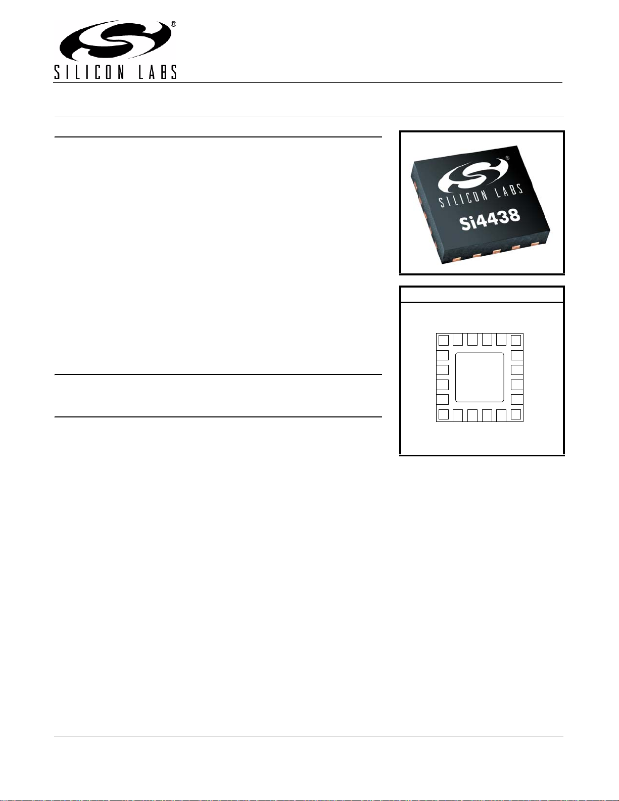
Silicon Laboratories EZRADIOPRO Si4438 User manual
Rev 1.0 6/14 Copyright © 2014 by Silicon Laboratories Si4438
Si4438
HIGH-PERFORMANCE, LOW-CURRENT TRANSCEIVER
Features
Applications
Description
Silicon Laboratories' Si4438 is a high-performance, low-current
transceivers covering the sub-GHz frequency bands from 425 to
525 MHz. The Si4438 is targeted at the Chinese smart meter market and
is especially suited for electric meters. This device is footprint- and
pin-compatible with the Si446x radios, which provide industry-leading
performance for worldwide sub-GHz applications. The radios are part of
the EZRadioPRO®family, which includes a complete line of transmitters,
receivers, and transceivers covering a wide range of applications. All
parts offer outstanding sensitivity of –124 dBm while achieving extremely
low active and standby current consumption. The 58 dB adjacent channel
selectivity with 12.5 kHz channel spacing ensures robust receive
operation in harsh RF conditions. The Si4438 offers exceptional output
power of up to +20 dBm with outstanding TX efficiency. The high output
power and sensitivity results in an industry-leading link budget of 144 dB
allowing extended ranges and highly robust communication links.
Frequency
range = 425–525 MHz
Receive sensitivity = –124 dBm
Modulation
(G)FSK
OOK
Max output power
+20 dBm
Low active power consumption
14 mA RX
Ultra low current powerdown
modes
30 nA shutdown, 50 nA standby
Data rate = 100 bps to 500 kbps
Fast wake and hop times
Power supply = 1.8 to 3.6 V
Excellent selectivity performance
58 dB adjacent channel
75 dB blocking at 1 MHz
Antenna diversity and T/R switch
control
Highly configurable packet handler
TX and RX 64 byte FIFOs
Auto frequency control (AFC)
Automatic gain control (AGC)
Low BOM
Low battery detector
Temperature sensor
20-Pin QFN package
IEEE 802.15.4g ready
China regulatory
China smart meters
Patents pending
Pin Assignments
GND
PAD
1
2
3
17181920
11
12
13
14
67 8 9
4
5
16
10
15
GND
GPIO1
nSEL
SDI
SDO
SCLKNC
SDN
TX
GPIO0
VDD
nIRQ
RXp
RXn
XIN
GPIO3
GPIO2
XOUT
TXRamp
VDD
Si4438
2 Rev 1.0
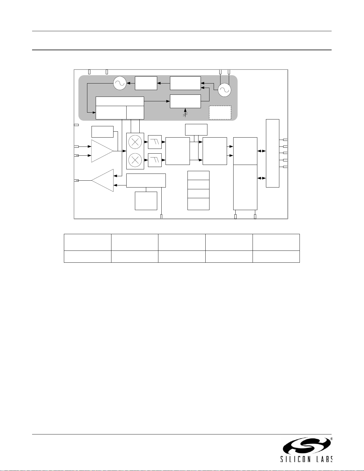
Functional Block Diagram
Product Freq. Range Max Output
Power TX Current RX Current
Si4438 425–525 MHz +20 dBm 75 mA 14 mA
VCO
Loop
Filter PFD / CP
Frac-N Div 30 MHz XO
LO
Gen
LNA
RF
PKDET
PGA ADC
MODEM
FIFO
Packet
Handler
32K LP
OSC
Bootup
OSC
LBD
POR
IF
PKDET
SPI Interface
Controller
Digital
Logic
PowerRamp
Cntl
PA
LDO
TX DIV
RXP
RXN
TX
VDD TXRAMP
XOUTXIN
nSEL
SDI
SDO
SCLK
nIRQ
LDOs
FBDIV
PA
VDD GPIO0 GPIO1
GPIO2GPIO3
SDN

Si4438
Rev 1.0 3
TABLE OF CONTENTS
Section Page
1. Electrical Specifications . . . . . . . . . . . . . . . . . . . . . . . . . . . . . . . . . . . . . . . . . . . . . . . . . . .4
2. Functional Description . . . . . . . . . . . . . . . . . . . . . . . . . . . . . . . . . . . . . . . . . . . . . . . . . . .11
3. Controller Interface . . . . . . . . . . . . . . . . . . . . . . . . . . . . . . . . . . . . . . . . . . . . . . . . . . . . . .12
3.1. Serial Peripheral Interface (SPI) . . . . . . . . . . . . . . . . . . . . . . . . . . . . . . . . . . . . . . . .12
3.2. Fast Response Registers . . . . . . . . . . . . . . . . . . . . . . . . . . . . . . . . . . . . . . . . . . . . .14
3.3. Operating Modes and Timing . . . . . . . . . . . . . . . . . . . . . . . . . . . . . . . . . . . . . . . . . .14
3.4. Application Programming Interface . . . . . . . . . . . . . . . . . . . . . . . . . . . . . . . . . . . . . .18
3.5. Interrupts . . . . . . . . . . . . . . . . . . . . . . . . . . . . . . . . . . . . . . . . . . . . . . . . . . . . . . . . . .18
3.6. GPIO . . . . . . . . . . . . . . . . . . . . . . . . . . . . . . . . . . . . . . . . . . . . . . . . . . . . . . . . . . . . .18
4. Modulation and Hardware Configuration Options . . . . . . . . . . . . . . . . . . . . . . . . . . . . .19
4.1. Modulation Types . . . . . . . . . . . . . . . . . . . . . . . . . . . . . . . . . . . . . . . . . . . . . . . . . . .19
4.2. Hardware Configuration Options . . . . . . . . . . . . . . . . . . . . . . . . . . . . . . . . . . . . . . . .19
4.3. Preamble Length . . . . . . . . . . . . . . . . . . . . . . . . . . . . . . . . . . . . . . . . . . . . . . . . . . . .20
5. Internal Functional Blocks . . . . . . . . . . . . . . . . . . . . . . . . . . . . . . . . . . . . . . . . . . . . . . . .22
5.1. RX Chain . . . . . . . . . . . . . . . . . . . . . . . . . . . . . . . . . . . . . . . . . . . . . . . . . . . . . . . . . .22
5.2. RX Modem . . . . . . . . . . . . . . . . . . . . . . . . . . . . . . . . . . . . . . . . . . . . . . . . . . . . . . . .22
5.3. Synthesizer . . . . . . . . . . . . . . . . . . . . . . . . . . . . . . . . . . . . . . . . . . . . . . . . . . . . . . . .24
5.4. Transmitter (TX) . . . . . . . . . . . . . . . . . . . . . . . . . . . . . . . . . . . . . . . . . . . . . . . . . . . .26
5.5. Crystal Oscillator . . . . . . . . . . . . . . . . . . . . . . . . . . . . . . . . . . . . . . . . . . . . . . . . . . . .29
6. Data Handling and Packet Handler . . . . . . . . . . . . . . . . . . . . . . . . . . . . . . . . . . . . . . . . . .30
6.1. RX and TX FIFOs . . . . . . . . . . . . . . . . . . . . . . . . . . . . . . . . . . . . . . . . . . . . . . . . . . .30
6.2. Packet Handler . . . . . . . . . . . . . . . . . . . . . . . . . . . . . . . . . . . . . . . . . . . . . . . . . . . . .30
7. RX Modem Configuration . . . . . . . . . . . . . . . . . . . . . . . . . . . . . . . . . . . . . . . . . . . . . . . . .32
8. Auxiliary Blocks . . . . . . . . . . . . . . . . . . . . . . . . . . . . . . . . . . . . . . . . . . . . . . . . . . . . . . . . .32
8.1. Wake-up Timer and 32 kHz Clock Source . . . . . . . . . . . . . . . . . . . . . . . . . . . . . . . .32
8.2. Low Duty Cycle Mode (Auto RX Wake-Up) . . . . . . . . . . . . . . . . . . . . . . . . . . . . . . .32
8.3. Temperature, Battery Voltage, and Auxiliary ADC . . . . . . . . . . . . . . . . . . . . . . . . . .34
8.4. Low Battery Detector . . . . . . . . . . . . . . . . . . . . . . . . . . . . . . . . . . . . . . . . . . . . . . . . .34
8.5. Antenna Diversity . . . . . . . . . . . . . . . . . . . . . . . . . . . . . . . . . . . . . . . . . . . . . . . . . . .34
9. Pin Descriptions: Si4438 . . . . . . . . . . . . . . . . . . . . . . . . . . . . . . . . . . . . . . . . . . . . . . . . . .35
10. Ordering Information . . . . . . . . . . . . . . . . . . . . . . . . . . . . . . . . . . . . . . . . . . . . . . . . . . . .37
11. Package Outline: Si4438 . . . . . . . . . . . . . . . . . . . . . . . . . . . . . . . . . . . . . . . . . . . . . . . . .38
12. PCB Land Pattern: Si4438 . . . . . . . . . . . . . . . . . . . . . . . . . . . . . . . . . . . . . . . . . . . . . . . .40
13. Top Marking . . . . . . . . . . . . . . . . . . . . . . . . . . . . . . . . . . . . . . . . . . . . . . . . . . . . . . . . . . .42
13.1. Si4438 Top Marking . . . . . . . . . . . . . . . . . . . . . . . . . . . . . . . . . . . . . . . . . . . . . . . .42
13.2. Top Marking Explanation . . . . . . . . . . . . . . . . . . . . . . . . . . . . . . . . . . . . . . . . . . . .42
Document Change List . . . . . . . . . . . . . . . . . . . . . . . . . . . . . . . . . . . . . . . . . . . . . . . . . . . . .43
Contact Information . . . . . . . . . . . . . . . . . . . . . . . . . . . . . . . . . . . . . . . . . . . . . . . . . . . . . . . .44

Si4438
4 Rev 1.0
1. Electrical Specifications
Table 1. DC Characteristics*
Parameter Symbol Test Condition Min Typ Max Unit
Supply Voltage
Range VDD 1.8 3.3 3.6 V
Power Saving Modes IShutdown RC Oscillator, Main Digital Regulator,
and Low Power Digital Regulator OFF —30—nA
IStandby Register values maintained and RC
oscillator/WUT OFF —50—nA
ISleepRC RC Oscillator/WUT ON and all register values main-
tained, and all other blocks OFF —900— nA
ISleepXO Sleep current using an external 32 kHz crystal. — 1.7 — µA
ISensor
-LBD Low battery detector ON, register values maintained,
and all other blocks OFF —1—µA
IReady Crystal Oscillator and Main Digital Regulator ON,
all other blocks OFF —1.8—mA
TUNE Mode Current ITune_RX RX Tune — 7.2 — mA
ITune_TX TX Tune — 8 — mA
RX Mode Current IRXH —14—mA
TX Mode Current
(Si4438) ITX_+20 +20 dBm output power, class-E match, 490 MHz,
3.3 V —75—mA
*Note: All minimum and maximum values are guaranteed by production test unless otherwise stated. All typical values apply at
VDD = 3.3 V and 25 °C unless otherwise stated.

Si4438
Rev 1.0 5
Table 2. Synthesizer AC Electrical Characteristics1
Parameter Symbol Test Condition Min Typ Max Unit
Synthesizer Frequency
Range (Si4438) FSYN 425 — 525 MHz
Synthesizer Frequency
Resolution2FRES-525 425–525 MHz —14.3— Hz
Synthesizer Settling Time tLOCK Measured from exiting Ready mode with
XOSC running to any frequency.
Including VCO Calibration.
—50— µs
Phase Noise L(fM)F = 10 kHz, 460 MHz — –106 — dBc/Hz
F = 100 kHz, 460 MHz — –110 — dBc/Hz
F=1MHz,460MHz — –123 — dBc/Hz
F = 10 MHz, 460 MHz — –130 — dBc/Hz
Notes:
1. All minimum and maximum values are guaranteed by production test unless otherwise stated. All typical values apply
at VDD = 3.3 V and 25 °C unless otherwise stated.
2. Default API setting for modulation deviation resolution is double the typical value specified.

Si4438
6 Rev 1.0
Table 3. Receiver AC Electrical Characteristics1
Parameter Symbol Test Condition Min Typ Max Unit
RX Frequency
Range (Si4438) FRX 425 — 525 MHz
RX Sensitivity PRX_0.5 (BER < 0.1%)
(500 bps, GFSK, BT = 0.5,
f=250Hz)2
—–124—dBm
PRX_40 (BER < 0.1%)
(40 kbps, GFSK, BT = 0.5,
f=20 kHz)2
—–108—dBm
PRX_100 (BER < 0.1%)
(100 kbps, GFSK, BT = 0.5,
f=50 kHz)1
—–103—dBm
PRX_9.6 (BER < 0.1%)
(9.6 kbps, GFSK, BT = 0.5,
f=4.8 kHz)2
—–114—dBm
PRX_OOK (BER < 0.1%, 4.8 kbps, 350 kHz BW,
OOK, PN15 data)2—–108—dBm
(BER < 0.1%, 40 kbps, 350 kHz BW,
OOK, PN15 data)2—–102—dBm
(BER < 0.1%, 120 kbps, 350 kHz BW,
OOK, PN15 data)2— –98 — dBm
RX Channel Bandwidth4BW 1.1 — 850 kHz
BER Variation vs Power
Level2PRX_RES Up to +5 dBm Input Level — 0 0.1 ppm
RSSI Resolution RESRSSI —±0.5— dB
1-Ch Offset Selectivity,
450 MHz2C/I1-CH Desired Ref Signal 3 dB above sensitiv-
ity, BER < 0.1%. Interferer is CW, and
desired is modulated with 2.4 kbps
F = 1.2 kHz GFSK with BT = 0.5, RX
channel BW = 4.8 kHz,
channel spacing = 12.5 kHz
— –58 — dB
Blocking 1 MHz Offset21MBLOCK Desired Ref Signal 3 dB above sensitiv-
ity, BER = 0.1%. Interferer is CW, and
desired is modulated with 2.4 kbps,
F = 1.2 kHz GFSK with BT = 0.5,
RX channel BW = 4.8 kHz
— –75 — dB
Blocking 8 MHz Offset28MBLOCK — –84 — dB
Image Rejection2ImREJ Rejection at the image frequency.
IF = 468 kHz —35—dB
Notes:
1. All minimum and maximum values are guaranteed by production test unless otherwise stated. All typical values apply at
VDD = 3.3 V and 25 °C unless otherwise stated.
2. BER is measured in the 450–470 MHz frequency band on RF evaluation boards.
3. For PER tests, 48 preamble symbols, 4 byte sync word, 10 byte payload and CRC-32 was used.
4. Guaranteed by bench characterization.

Si4438
Rev 1.0 7
Table 4. Transmitter AC Electrical Characteristics1
Parameter Symbol Test Condition Min Typ Max Unit
TX Frequency
Range FTX 425 — 525 MHz
(G)FSK Data Rate2,3 DRFSK 0.1 — 500 kbps
OOK Data Rate2,3 DROOK 0.1 — 120 kbps
Modulation Deviation
Range f525 425–525 MHz —750—kHz
Modulation Deviation
Resolution4FRES-525 425–525 MHz —14.3 —Hz
Output Power Range5PTX –20 — +20 dBm
TX RF Output Steps PRF_OUT Using switched current match within
6 dB of max power —0.1—dB
TX RF Output Level
Variation vs. Temperature PRF_TEMP –40 to +85 C—1—dB
TX RF Output Level
Variation vs. Frequency PRF_FREQ —0.5—dB
Transmit Modulation
Filtering B*T Gaussian Filtering Bandwith Time
Product —0.5—
Notes:
1. All minimum and maximum values are guaranteed by production test unless otherwise stated. All typical values apply at
VDD = 3.3 V and 25 °C unless otherwise stated.
2. Guaranteed by design.
3. The maximum data rate is dependent on the XTAL frequency and is calculated as per the formula:
Maximum Symbol Rate = Fxtal/60, where Fxtal is the XTAL frequency (typically 30 MHz).
4. Default API setting for modulation deviation resolution is double the typical value specified.
5. Output power is dependent on matching components and board layout.

Si4438
8 Rev 1.0
Table 5. Auxiliary Block Specifications1
Parameter Symbol Test Condition Min Typ Max Unit
Temperature Sensor
Sensitivity TSS— 4.5 — ADC
Codes/
°C
Low Battery Detector
Resolution LBDRES —50—mV
Microcontroller Clock
Output Frequency Range2FMC Configurable to Fxtal or Fxtal
divided by 2, 3, 7.5, 10, 15, or
30 where Fxtal is the reference
XTAL frequency. In addition,
32.768 kHz is also supported.
32.768K — Fxtal Hz
Temperature Sensor
Conversion TEMPCT Programmable setting — 3 — ms
XTAL Range3XTALRange 25 — 32 MHz
30 MHz XTAL Start-Up Time t30M Using XTAL and board layout in
reference design. Start-up time
will vary with XTAL type and
board layout.
— 250 — µs
30 MHz XTAL Cap
Resolution 30MRES —70—fF
32 kHz XTAL Start-Up Time t32k —2—sec
32 kHz Accuracy using
Internal RC Oscillator 32KRCRES — 2500 — ppm
POR Reset Time tPOR ——5ms
Notes:
1. All minimum and maximum values are guaranteed by production test unless otherwise stated. All typical values apply at
VDD = 3.3 V and 25 °C unless otherwise stated.
2. Microcontroller clock frequency tested in production at 1 MHz, 30 MHz and 32.768 kHz. Other frequencies tested in
bench characterization.
3. XTAL Range tested in production using an external clock source (similar to using a TCXO).

Si4438
Rev 1.0 9
Table 6. Digital IO Specifications (GPIO_x, SCLK, SDO, SDI, nSEL, nIRQ, SDN)1
Parameter Symbol Test Condition Min Typ Max Unit
Rise Time2,3 TRISE 0.1 x VDD to 0.9 x VDD,
CL=10pF,
DRV<1:0> = LL
—2.3— ns
Fall Time3,4 TFALL 0.9 x VDD to 0.1 x VDD,
CL=10pF,
DRV<1:0> = LL
—2—ns
Input Capacitance CIN —2—pF
Logic High Level Input Voltage VIH VDD x0.7 — — V
Logic Low Level Input Voltage VIL ——V
DD x0.3 V
Input Current IIN 0<VIN< VDD –10 — 10 µA
Input Current If Pullup is Activated IINP VIL =0V 1 — 10 µA
Drive Strength for Output Low
Level IOmaxLL DRV[1:0] = LL3—6.66— mA
IOmaxLH DRV[1:0] = LH3—5.03— mA
IOmaxHL DRV[1:0] = HL3—3.16— mA
IOmaxHH DRV[1:0] = HH3—1.13— mA
Drive Strength for Output High
Level IOmaxLL DRV[1:0] = LL3—5.75— mA
IOmaxLH DRV[1:0] = LH3—4.37— mA
IOmaxHL DRV[1:0] = HL3—2.73— mA
IOmaxHH DRV[1:0] = HH3—0.96— mA
Drive Strength for Output High
Level for GPIO0 IOmaxLL DRV[1:0] = LL3—2.53— mA
IOmaxLH DRV[1:0] = LH3—2.21— mA
IOmaxHL DRV[1:0] = HL3—1.7—mA
IOmaxHH DRV[1:0] = HH3—0.80— mA
Logic High Level Output Voltage VOH DRV[1:0] = HL VDD x0.8 — — V
Logic Low Level Output Voltage VOL DRV[1:0] = HL — — VDD x0.2 V
Notes:
1. All minimum and maximum values are guaranteed by production test unless otherwise stated. All typical values apply
at VDD = 3.3 V and 25 °C unless otherwise stated.
2. 8 ns is typical for GPIO0 rise time.
3. Assuming VDD = 3.3 V, drive strength is specified at Voh (min) = 2.64 V and Vol(max) = 0.66 V at room temperature.
4. 2.4 ns is typical for GPIO0 fall time.

Si4438
10 Rev 1.0
Table 7. Thermal Operating Characteristics
Parameter Value Unit
Operating Ambient Temperature Range TA–40 to +85 C
Thermal Impedance JA 30 C/W
Junction Temperature TJMAX +125 C
Storage Temperature Range TSTG –55 to +125 C
Table 8. Absolute Maximum Ratings*
Parameter Value Unit
VDD to GND –0.3, +3.6 V
Instantaneous VRF-peak to GND on TX Output Pin –0.3, +8.0 V
Sustained VRF-peak to GND on TX Output Pin –0.3, +6.5 V
Voltage on Digital Control Inputs –0.3, VDD + 0.3 V
Voltage on Analog Inputs –0.3, VDD + 0.3 V
Voltage on XIN Input when using a TCXO –0.7, VDD + 0.3 V
RX Input Power +10 dBm
Operating Ambient Temperature Range TA–40 to +85 C
Thermal Impedance JA 30 C/W
Junction Temperature TJ+125 C
Storage Temperature Range TSTG –55 to +125 C
*Note: Stresses beyond those listed under “Absolute Maximum Ratings” may cause permanent damage to the device. These
are stress ratings only and functional operation of the device at or beyond these ratings in the operational sections of
the specifications is not implied. Exposure to absolute maximum rating conditions for extended periods may affect
device reliability. Power Amplifier may be damaged if switched on without proper load or termination connected. TX
matching network design will influence TX VRF-peak on TX output pin. Caution: ESD sensitive device.

Si4438
Rev 1.0 11
2. Functional Description
The Si4438 devices are high-performance, low-current, wireless ISM transceivers that cover the sub-GHz bands.
The wide operating voltage range of 1.8–3.6 V and low current consumption make the Si4438 an ideal solution for
battery powered applications. The Si4438 operates as a time division duplexing (TDD) transceiver where the
device alternately transmits and receives data packets. The device uses a single-conversion mixer to downconvert
the 2-level FSK/GFSK or OOK modulated receive signal to a low IF frequency. Following a programmable gain
amplifier (PGA) the signal is converted to the digital domain by a high performance ADC allowing filtering,
demodulation, slicing, and packet handling to be performed in the built-in DSP increasing the receiver’s
performance and flexibility versus analog based architectures. The demodulated signal is output to the system
MCU through a programmable GPIO or via the standard SPI bus by reading the 64-byte RX FIFO.
A single high precision local oscillator (LO) is used for both transmit and receive modes since the transmitter and
receiver do not operate at the same time. The LO is generated by an integrated VCO and Fractional-N PLL
synthesizer. The synthesizer is designed to support configurable data rates from 100 bps to 500 kbps. The transmit
FSK data is modulated directly into the data stream and can be shaped by a Gaussian low-pass filter to reduce
unwanted spectral content.
The Si4438 contains a power amplifier (PA) that supports output power up to +20 dBm with very high efficiency,
consuming only 75 mA. The integrated +20 dBm power amplifier can also be used to compensate for the reduced
performance of a lower cost, lower performance antenna or antenna with size constraints due to a small
form-factor. Competing solutions require large and expensive external PAs to achieve comparable performance.
The PA is single-ended to allow for easy antenna matching and low BOM cost. The PA incorporates automatic
ramp-up and ramp-down control to reduce unwanted spectral spreading. The Si4438 family supports TX/RX switch
control, and antenna diversity switch control to extend the link range and improve performance. Built-in antenna
diversity can be used to further extend range and enhance performance. Antenna diversity is completely integrated
into the Si4438 and can improve the system link budget by 8–10 dB, resulting in substantial range increases under
adverse environmental conditions. A highly configurable packet handler allows for autonomous encoding/decoding
of nearly any packet structure. Additional system features, such as an automatic wake-up timer, low battery
detector, 64 byte TX/RX FIFOs, and preamble detection, reduce overall current consumption and allows for the
use of lower-cost system MCUs. An integrated temperature sensor, power-on-reset (POR), and GPIOs further
reduce overall system cost and size. The Si4438 is designed to work with an MCU, crystal, and a few passive
components to create a very low-cost system.
Si4438
12 Rev 1.0
3. Controller Interface
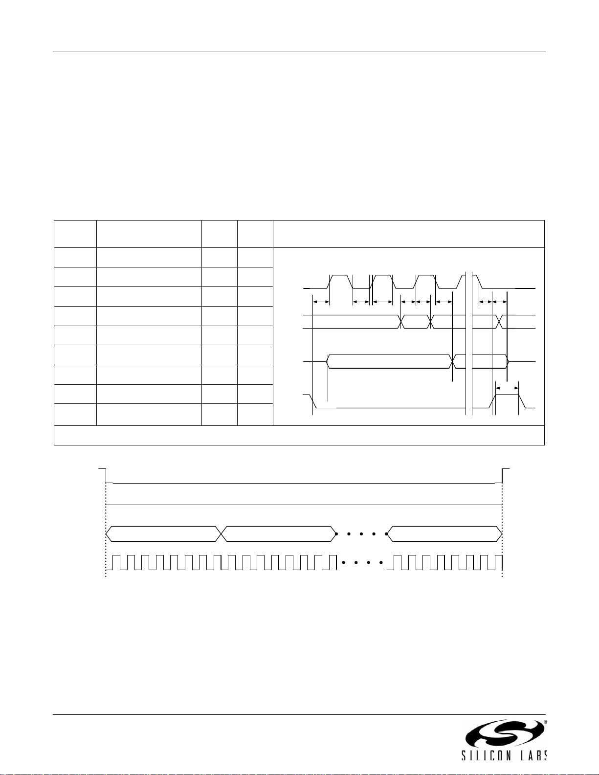
3.1. Serial Peripheral Interface (SPI)
The Si4438 communicates with the host MCU over a standard 4-wire serial peripheral interface (SPI): SCLK, SDI,
SDO, and nSEL. The SPI interface is designed to operate at a maximum of 10 MHz. The SPI timing parameters
are demonstrated in Table 9. The host MCU writes data over the SDI pin and can read data from the device on the
SDO output pin. Figure 1 demonstrates an SPI write command. The nSEL pin should go low to initiate the SPI
command. The first byte of SDI data will be one of the firmware commands followed by n bytes of parameter data
which will be variable depending on the specific command. The rising edges of SCLK should be aligned with the
center of the SDI data.
Figure 1. SPI Write Command
The Si4438 contains an internal MCU which controls all the internal functions of the radio. For SPI read commands
a typical MCU flow of checking clear-to-send (CTS) is used to make sure the internal MCU has executed the
command and prepared the data to be output over the SDO pin. Figure 2 demonstrates the general flow of an SPI
read command. Once the CTS value reads FFh then the read data is ready to be clocked out to the host MCU. The
typical time for a valid FFh CTS reading is 20 µs. Figure 3 demonstrates the remaining read cycle after CTS is set
to FFh. The internal MCU will clock out the SDO data on the negative edge so the host MCU should process the
SDO data on the rising edge of SCLK.
Table 9. Serial Interface Timing Parameters
Symbol Parameter Min
(ns) Max
(ns) Diagram
tCH Clock high time 40
tCL Clock low time 40
tDS Data setup time 20
tDH Data hold time 20
tDD Output data delay time 43
tDE Output disable time 45
tSS Select setup time 20
tSH Select hold time 50
tSW Select high period 80
*Note: CL = 10 pF; VDD = 1.8 V; SDO Drive strength setting = 10.
SCLK
SDI
SDO
nSEL
tCL
tSS tCH tDS tDH tDD tSH tDE
tSW
FW Command ParamByte 0 Param Byte n
nSEL
SDO
SDI
SCLK

Si4438
Rev 1.0 13
Figure 2. SPI Read Command—Check CTS Value
Figure 3. SPI Read Command—Clock Out Read Data
Send Command Read CTS Retrieve
Response
CTS Value
0x00
0xFF
Firmware Flow
ReadCmdBuff
NSEL
SDO
SDI
SCK
CTS
NSEL
SDO
SDI
SCK
Response Byte 0 Response Byte n

Si4438
14 Rev 1.0
3.2. Fast Response Registers
The fast response registers are registers that can be read immediately without the requirement to monitor and
check CTS. There are four fast response registers that can be programmed for a specific function. The fast
response registers can be read through API commands, 0x50 for Fast Response A, 0x51 for Fast Response B,
0x53 for Fast Response C, and 0x57 for Fast Response D. The fast response registers can be configured by the
“FRR_CTL_X_MODE” properties.
The fast response registers may be read in a burst fashion. After the initial 16 clock cycles, each additional eight
clock cycles will clock out the contents of the next fast response register in a circular fashion. The value of the
FRRs will not be updated unless NSEL is toggled.
3.3. Operating Modes and Timing
The primary states of the Si4438 are shown in Figure 4. The shutdown state completely shuts down the radio to
minimize current consumption. Standby/Sleep, SPI Active, Ready, TX Tune, and RX tune are available to optimize
the current consumption and response time to RX/TX for a given application. API commands START_RX,
START_TX, and CHANGE_STATE control the operating state with the exception of shutdown which is controlled
by SDN, pin 1. Table 10 shows each of the operating modes with the time required to reach either RX or TX mode
as well as the current consumption of each mode. The times in Table 9 are measured from the rising edge of nSEL
until the chip is in the desired state. Note that these times are indicative of state transition timing but are not
guaranteed and should only be used as a reference data point. An automatic sequencer will put the chip into RX or
TX from any state. It is not necessary to manually step through the states. To simplify the diagram it is not shown
but any of the lower power states can be returned to automatically after RX or TX.
Figure 4. State Machine Diagram

Si4438
Rev 1.0 15
Figure 5 shows the POR timing and voltage requirements. The power consumption (battery life) depends on the
duty cycle of the application or how often the part is in either Rx or Tx state. In most applications the utilization of
the standby state will be most advantageous for battery life but for very low duty cycle applications shutdown will
have an advantage. For the fastest timing the next state can be selected in the START_RX or START_TX API
commands to minimize SPI transactions and internal MCU processing.
3.3.1. Power on Reset (POR)
A Power On Reset (POR) sequence is used to boot the device up from a fully off or shutdown state. To execute this
process, VDD must ramp within 1ms and must remain applied to the device for at least 10ms. If VDD is removed,
then it must stay below 0.15V for at least 10ms before being applied again. Please see Figure x and Table x for
details.
Figure 5. POR Timing Diagram
Table 10. Operating State Response Time and Current Consumption
State/Mode Response Time to Current in State
/Mode
TX RX
ShutdownState 15ms 15ms 30nA
Standby State
Sleep State
SPI Active State
Ready State
TX Tune State
RX Tune State
440 µs
440 µs
340 µs
126 µs
58 µs
—
440 µs
440 µs
340 µs
122 µs
—
74 µs
50 nA
900 nA
1.35 mA
1.8 mA
8mA
7.2 mA
TXState — 138µs 75mA@+20dBm
RX State 130 µs 75 µs 14 mA
VDD
Time
VRRH
tSR tPORH
VRRL

Si4438
16 Rev 1.0
3.3.2. Shutdown State
The shutdown state is the lowest current consumption state of the device with nominally less than 30 nA of current
consumption. The shutdown state may be entered by driving the SDN pin (Pin 1) high. The SDN pin should be held
low in all states except the shutdown state. In the shutdown state, the contents of the registers are lost and there is
no SPI access. When coming out of the shutdown state a power on reset (POR) will be initiated along with the
internal calibrations. After the POR the POWER_UP command is required to initialize the radio. The SDN pin
needs to be held high for at least 10us before driving low again so that internal capacitors can discharge. Not
holding the SDN high for this period of time may cause the POR to be missed and the device to boot up incorrectly.
If POR timing and voltage requirements cannot be met, it is highly recommended that SDN be controlled using the
host processor rather than tying it to GND on the board.
3.3.3. Standby State
Standby state has the lowest current consumption with the exception of shutdown but has much faster response
time to RX or TX mode. In most cases standby should be used as the low power state. In this state the register
values are maintained with all other blocks disabled. The SPI is accessible during this mode but any SPI event,
including FIFO R/W, will enable an internal boot oscillator and automatically move the part to SPI active state. After
an SPI event the host will need to re-command the device back to standby through the “Change State” API
command to achieve the 50 nA current consumption. If an interrupt has occurred (i.e., the nIRQ pin = 0) the
interrupt registers must be read to achieve the minimum current consumption of this mode.
3.3.4. Sleep State
Sleep state is the same as standby state but the wake-up-timer and a 32 kHz clock source are enabled. The
source of the 32 kHz clock can either be an internal 32 kHz RC oscillator which is periodically calibrated or a
32 kHz oscillator using an external XTAL.The SPI is accessible during this mode but an SPI event will enable an
internal boot oscillator and automatically move the part to SPI active mode. After an SPI event the host will need to
re-command the device back to sleep. If an interrupt has occurred (i.e., the nIRQ pin = 0) the interrupt registers
must be read to achieve the minimum current consumption of this mode.
3.3.5. SPI Active State
In SPI active state the SPI and a boot up oscillator are enabled. After SPI transactions during either standby or
sleep the device will not automatically return to these states. A “Change State” API command will be required to
return to either the standby or sleep modes.
3.3.6. Ready State
Ready state is designed to give a fast transition time to TX or RX state with reasonable current consumption. In this
mode the Crystal oscillator remains enabled reducing the time required to switch to TX or RX mode by eliminating
the crystal start-up time.
3.3.7. TX State
The TX state may be entered from any of the state with the “Start TX” or “Change State” API commands. A built-in
sequencer takes care of all the actions required to transition between states from enabling the crystal oscillator to
ramping up the PA. The following sequence of events will occur automatically when going from standby to TX state.
1. Enable internal LDOs.
2. Start up crystal oscillator and wait until ready (controlled by an internal timer).
Table 11. POR Timing
Variable Description Min Typ Max Units
tPORH High time for VDD to fully settle POR circuit 10 ms
tPORL Low time for VDD to enable POR 10 ms
VRRH Voltage for successful POR 90%*Vdd V
VRRL Starting Voltage for successful POR 0150mV
tSR Slew rate of VDD for successful POR 1ms

Si4438
Rev 1.0 17
3. Enable PLL.
4. Calibrate VCO/PLL.
5. Wait until PLL settles to required transmit frequency (controlled by an internal timer).
6. Activate power amplifier and wait until power ramping is completed (controlled by an internal timer).
7. Transmit packet.
Steps in this sequence may be eliminated depending on which state the chip is configured to prior to commanding
to TX. By default, the VCO and PLL are calibrated every time the PLL is enabled. When the START_TX API
command is utilized the next state may be defined to ensure optimal timing and turnaround.
Figure 6 shows an example of the commands and timing for the START_TX command. CTS will go high as soon
as the sequencer puts the part into TX state. As the sequencer is stepping through the events listed above, CTS
will be low and no new commands or property changes are allowed. If the Fast Response (FRR) or nIRQ is used to
monitor the current state there will be slight delay caused by the internal hardware from when the event actually
occurs to when the transition occurs on the FRR or nIRQ. The time from entering TX state to when the FRR will
update is 5 µs and the time to when the nIRQ will transition is 13 µs. If a GPIO is programmed for TX state or used
as control for a transmit/receive switch (TR switch) there is no delay.
Figure 6. Start_TX Commands and Timing
3.3.8. RX State
The RX state may be entered from any of the other states by using the “Start RX” or “Change State” API command.
A built-in sequencer takes care of all the actions required to transition between states. The following sequence of
events will occur automatically to get the chip into RX mode when going from standby to RX state:
1. Enable the digital LDO and the analog LDOs.
2. Start up crystal oscillator and wait until ready (controlled by an internal timer).
3. Enable PLL.
4. Calibrate VCO
5. Wait until PLL settles to required receive frequency (controlled by an internal timer).
6. Enable receiver circuits: LNA, mixers, and ADC.
7. Enable receive mode in the digital modem.
Depending on the configuration of the radio, all or some of the following functions will be performed automatically
by the digital modem: AGC, AFC (optional), update status registers, bit synchronization, packet handling (optional)
including sync word, header check, and CRC. Similar to the TX state, the next state after RX may be defined in the
“Start RX” API command. The START_RX commands and timing will be equivalent to the timing shown in Figure 6.
START_TX
CTS
NSEL
SDI
YYY State
Current State Tx State
nIRQ
YYY State
FRR Tx State TXCOMPLETE_STATE
TXCOMPLETE_STATE
GPIOx – TX state

Si4438
18 Rev 1.0
3.4. Application Programming Interface
The host MCU communicates with an application programming interface (API) embedded inside the device. The
API is divided into two sections, commands and properties. The commands are used to control the chip and
retrieve its status. The properties are general configurations which will change infrequently. For API description
details, refer to the EZRadioPRO API Documentation.zip file available on www.silabs.com.
3.5. Interrupts
The Si4438 is capable of generating an interrupt signal when certain events occur. The chip notifies the
microcontroller that an interrupt event has occurred by setting the nIRQ output pin LOW = 0. This interrupt signal
will be generated when any one (or more) of the interrupt events (corresponding to the Interrupt Status bits) occur.
The nIRQ pin will remain low until the microcontroller clears all the interrupts. The nIRQ output signal will then be
reset until the next change in status is detected.
The interrupts sources are grouped into three groups: packet handler, chip status, and modem. The individual
interrupts in these groups can be enabled/disabled in the interrupt property registers. An interrupt must be enabled
for it to trigger an event on the nIRQ pin. The interrupt group must be enabled as well as the individual interrupts in
API properties described in the API documentation. Once an interrupt event occurs and the nIRQ pin is low there
are two ways to read and clear the interrupts. All of the interrupts may be read and cleared in the
“GET_INT_STATUS” API command. By default all interrupts will be cleared once read. If only specific interrupts
want to be read in the fastest possible method the individual interrupt groups (Packet Handler, Chip Status,
Modem) may be read and cleared by the “GET_MODEM_STATUS”, “GET_PH_STATUS” (packet handler), and
“GET_CHIP_STATUS” API commands. The instantaneous status of a specific function maybe read if the specific
interrupt is enabled or disabled. The status results are provided after the interrupts and can be read with the same
commands as the interrupts. The status bits will give the current state of the function whether the interrupt is
enabled or not. The fast response registers can also give information about the interrupt groups but reading the
fast response registers will not clear the interrupt and reset the nIRQ pin.
3.6. GPIO
Four general purpose IO pins are available to utilize in the application. The GPIO are configured by the
GPIO_PIN_CFG command in address 13h. For a complete list of the GPIO options please see the API guide.
GPIO pins 0 and 1 should be used for active signals such as data or clock. GPIO pins 2 and 3 have more
susceptibility to generating spurious in the synthesizer than pins 0 and 1. The drive strength of the GPIOs can be
adjusted with the GEN_CONFIG parameter in the GPIO_PIN_CFG command. By default the drive strength is set
to minimum. The default configuration for the GPIOs and the state during SDN is shown below in Table 12.The
state of the IO during shutdown is also shown in Table 12. As indicated previously in Table 6, GPIO 0 has lower
drive strength than the other GPIOs.
Table 12. GPIOs
Pin SDN State POR Default
GPIO0 0 POR
GPIO1 0 CTS
GPIO2 0 POR
GPIO3 0 POR
nIRQ resistive VDD pull-up nIRQ
SDO resistive VDD pull-up SDO
SDI High Z SDI
SCLK High Z SCLK
NSEL High Z NSEL

Si4438
Rev 1.0 19
4. Modulation and Hardware Configuration Options
The Si4438 supports three different modulation options and can be used in various configurations to tailor the
device to any specific application or legacy system for drop in replacement. The modulation and configuration
options are set in property, MODEM_MOD_TYPE. Refer to the EZRadioPRO API Documentation.zip file available
on www.silabs.com for details.
4.1. Modulation Types
The Si4438 supports five different modulation options: Gaussian frequency shift keying (GFSK), frequency-shift
keying (FSK), on-off keying (OOK). Minimum shift keying (MSK) can also be created by using GFSK settings.
GFSK is the recommended modulation type as it provides the best performance and cleanest modulation
spectrum. The modulation type is set by the “MOD_TYPE[2:0]” registers in the “MODEM_MOD_TYPE” API
property. A continuous-wave (CW) carrier may also be selected for RF evaluation purposes. The modulation
source may also be selected to be a pseudo-random source for evaluation purposes.
4.2. Hardware Configuration Options
There are different receive demodulator options to optimize the performance and mutually-exclusive options for
how the RX/TX data is transferred from the host MCU to the RF device.
4.2.1. Receive Demodulator Options
There are multiple demodulators integrated into the device to optimize the performance for different applications,
modulation formats, and packet structures. The calculator built into WDS will choose the optimal demodulator
based on the input criteria.
4.2.1.1. Synchronous Demodulator
The synchronous demodulator's internal frequency error estimator acquires the frequency error based on a
101010 preamble structure. The bit clock recovery circuit locks to the incoming data stream within four transactions
of a “10” or “01” bit stream. The synchronous demodulator gives optimal performance for 2-level FSK or GFSK
modulation that has a modulation index less than 2.
4.2.1.2. Asynchronous Demodulator
The asynchronous demodulator should be used OOK modulation and for FSK/GFSK under one or more of the
following conditions:
Modulation index > 2
Non-standard preamble (not 1010101... pattern)
When the modulation index exceeds 2, the asynchronous demodulator has better sensitivity compared to the
synchronous demodulator. An internal deglitch circuit provides a glitch-free data output and a data clock signal to
simplify the interface to the host. There is no requirement to perform deglitching in the host MCU. The
asynchronous demodulator will typically be utilized for legacy systems and will have many performance benefits
over devices used in legacy designs. Unlike the Si4432/31 solution for non-standard packet structures, there is no
requirement to perform deglitching on the data in the host MCU. Glitch-free data is output from Si4438 devices,
and a sample clock for the asynchronous data can also be supplied to the host MCU; so, oversampling or bit clock
recovery is not required by the host MCU. There are multiple detector options in the asynchronous demodulator
block, which will be selected based upon the options entered into the WDS calculator. The asynchronous
demodulator's internal frequency error estimator is able to acquire the frequency error based on any preamble
structure.
4.2.2. RX/TX Data Interface With MCU
There are two different options for transferring the data from the RF device to the host MCU. FIFO mode uses the
SPI interface to transfer the data, while direct mode transfers the data in real time over GPIO.
4.2.2.1. FIFO Mode
In FIFO mode, the transmit and receive data is stored in integrated FIFO register memory. The TX FIFO is
accessed by writing Command 66h followed directly by the data/clk that the host wants to write into the TX FIFO.
The RX FIFO is accessed by writing command 77h followed by the number of clock cycles of data the host would
like to read out of the RX FIFO. The RX data will be clocked out onto the SDO pin.

Si4438
20 Rev 1.0
In TX mode, if the packet handler is enabled, the data bytes stored in FIFO memory are “packaged” together with
other fields and bytes of information to construct the final transmit packet structure. These other potential fields
include the Preamble, Sync word, Header, CRC checksum, etc. The configuration of the packet structure in TX
mode is determined by the Automatic Packet Handler (if enabled), in conjunction with a variety of Packet Handler
properties. If the Automatic Packet Handler is disabled, the entire desired packet structure should be loaded into
FIFO memory; no other fields (such as Preamble or Sync word) will be automatically added to the bytes stored in
FIFO memory. For further information on the configuration of the FIFOs for a specific application or packet size,
see "6. Data Handling and Packet Handler" on page 30. In RX mode, only the bytes of the received packet
structure that are considered to be “data bytes” are stored in FIFO memory. Which bytes of the received packet are
considered “data bytes” is determined by the Automatic Packet Handler (if enabled) in conjunction with the Packet
Handler configuration. If the Automatic Packet Handler is disabled, all bytes following the Sync word are
considered data bytes and are stored in FIFO memory. Thus, even if Automatic Packet Handling operation is not
desired, the preamble detection threshold and Sync word still need to be programmed so that the RX Modem
knows when to start filling data into the FIFO. When the FIFO is being used in RX mode, all of the received data
may still be observed directly (in realtime) by properly programming a GPIO pin as the RXDATA output pin; this can
be quite useful during application development. When in FIFO mode, the chip will automatically exit the TX or RX
State when either the PACKET_SENT or PACKET_RX interrupt occurs. The chip will return to the IDLE state
programmed in the argument of the “START TX” or “START RX” API command, TXCOMPLETE_STATE[3:0] or
RXVALID_STATE[3:0]. For example, the chip may be placed into TX mode by sending the “START TX” command
and by writing the 30h to the TXCOMPLETE_STATE[3:0] argument. The chip will transmit all of the contents of the
FIFO, and the ipksent interrupt will occur. When this event occurs, the chip will return to the ready state as defined
by TXCOMPLETE_STATE[3:0] = 30h.
4.2.2.2. Direct Mode
For legacy systems that perform packet handling within the host MCU or other baseband chip, it may not be
desirable to use the FIFO. For this scenario, a Direct mode is provided, which bypasses the FIFOs entirely. In TX
Direct mode, the TX modulation data is applied to an input pin of the chip and processed in “real time” (i.e., not
stored in a register for transmission at a later time). Any of the GPIOs may be configured for use as the TX Data
input function. Furthermore, an additional pin may be required for a TX Clock output function if GFSK modulation is
desired (only the TX Data input pin is required for FSK). To achieve direct mode, the GPIO must be configured in
the “GPIO_PIN_CFG” API command as well as the “MODEM_MOD_TYPE” API property. For GFSK,
“TX_DIRECT_MODE_TYPE” must be set to Synchronous. For 2FSK or OOK, the type can be set to asynchronous
or synchronous. The MOD_SOURCE[1:0] should be set to 01h for are all direct mode configurations. In RX Direct
mode, the RX Data and RX Clock can be programmed for direct (real-time) output to GPIO pins. The
microcontroller may then process the RX data without using the FIFO or packet handler functions of the RFIC.
4.3. Preamble Length
The preamble length requirement is only relevant if using the synchronous demodulator. If the asynchronous
demodulator is being used, then there is no requirement for a conventional 101010 pattern.
The preamble detection threshold determines the number of valid preamble bits the radio must receive to qualify a
valid preamble. The preamble threshold should be adjusted depending on the nature of the application. The
required preamble length threshold depends on when receive mode is entered in relation to the start of the
transmitted packet and the length of the transmit preamble. With a shorter than recommended preamble detection
threshold, the probability of false detection is directly related to how long the receiver operates on noise before the
transmit preamble is received. False detection on noise may cause the actual packet to be missed. The preamble
detection threshold may be adjusted in the modem calculator by modifying the “PM detection threshold” in the “RX
parameters tab” in the radio control panel. For most applications with a preamble length longer than 32 bits, the
default value of 20 is recommended for the preamble detection threshold. A shorter Preamble Detection Threshold
may be chosen if occasional false detections may be tolerated. When antenna diversity is enabled, a 20- bit
preamble detection threshold is recommended. When the receiver is synchronously enabled just before the start of
the packet, a shorter preamble detection threshold may be used. Table 13 demonstrates the recommended
preamble detection threshold and preamble length for various modes.
This manual suits for next models
1
Table of contents
Other Silicon Laboratories Transceiver manuals

Silicon Laboratories
Silicon Laboratories Si4432 User manual

Silicon Laboratories
Silicon Laboratories Si4432 User manual

Silicon Laboratories
Silicon Laboratories Si4430 User manual

Silicon Laboratories
Silicon Laboratories Si4455 Series User manual

Silicon Laboratories
Silicon Laboratories SI4421 User manual

Silicon Laboratories
Silicon Laboratories Si4468/7 User manual

Silicon Laboratories
Silicon Laboratories Si4355 Operating instructions

Silicon Laboratories
Silicon Laboratories Si4438-C User manual


