Skyworks Si5332-AM1 User manual

Si5332-AM1/2/3 Automotive Grade Device
Reference Manual
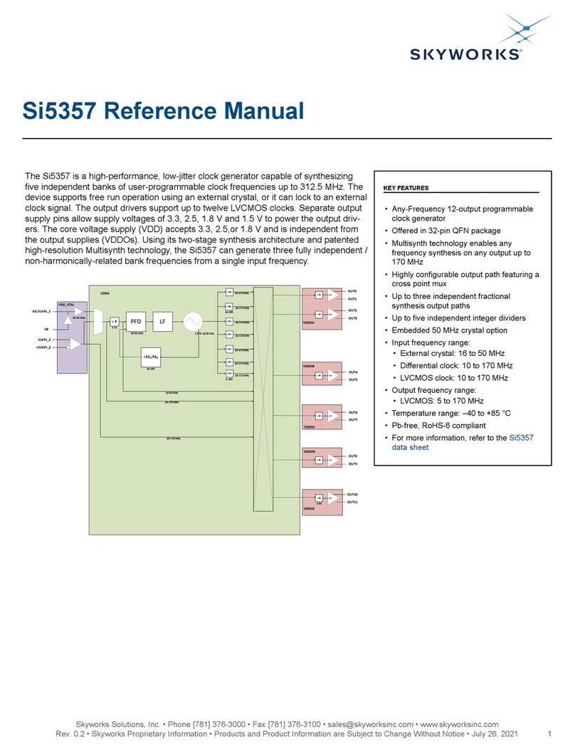
The Si5332-AM1/2/3 is a family of high-performance, low-jitter clock generators capable
of synthesizing five independent banks of user-programmable clock frequencies up to
333.33 MHz, while providing up to 12 differential or 24 single-ended output clocks.
The Si5332 supports free run operation using an external crystal as well as lock to an
external clock signal. The output drivers are configurable to support common signal for-
mats, such as LVPECL, LVDS, HCSL, and LVCMOS. Separate output supply pins allow
supply voltages of 3.3 V, 2.5 V, 1.8 V and 1.5 V (CMOS only) to power the multi-format
output drivers. The core voltage supply (VDD) accepts 3.3 V, 2.5 V, or 1.8 V and is inde-
pendent from the output supplies (VDDOs). Using its two-stage synthesis architecture
and patented high-resolution Multisynth technology, the Si5332 can generate three fully
independent/non-harmonically-related bank frequencies from a single input frequency.
÷ P PFD LF
÷Mn/Md
÷R
÷R
÷R
÷R
÷R
÷R
÷R
÷R
÷R
÷R
÷R
÷R
÷N0
÷N1
÷O0
÷O1
÷O2
÷O3
÷O4
1-31
10-255
10-50 MHz 2.375-2.625 GHz
10-255
8-255
10-250 MHz
10-250 MHz
10-312.5 MHz
10-312.5 MHz
10-312.5 MHz
10-312.5 MHz
10-312.5 MHz
1-63
10-50 MHz
10-250 MHz
10-250 MHz
10-250 MHz
10-30 MHz
VDD_XTAL
VDDA
VDDOA
VDDOB
VDDOC
VDDOD
VDDOE
XA/CLKIN_1
XB
CLKIN_2
nCLKIN_2
CLKIN_3
nCLKIN_3
OUT0
OUT1
OUT2
OUT3
OUT4
OUT5
OUT6
OUT7
OUT8
OUT9
OUT10
OUT11
RELATED DOCUMENTS
• Any-Frequency 6/8/12-output
programmable clock generators
• Offered in three different package sizes,
supporting different combinations of output
clocks and user configurable hardware
input pins
• 32-pin QFN, up to 6 outputs
• 40-pin QFN, up to 8 outputs
• 48-pin QFN, up to 12 outputs
• Multisynth technology enables any
frequency synthesis on any output up to
250 MHz using N dividers.
• Output frequencies up to 333.33 MHz
using O dividers.
• Highly configurable output path featuring a
cross point mux
• Up to three independent fractional
synthesis output paths
• Up to five independent integer dividers
• Down and center spread spectrum
• Input frequency range:
• External crystal: 16 MHz to 50 MHz
• Differential clock: 10 MHz to 250 MHz
• LVCMOS clock: 10 MHz to 170 MHz
• Output frequency range:
• Differential: 5 MHz to 333.33 MHz
• LVCMOS: 5 MHz to 170 MHz
• User-configurable clock output signal
format per output: LVDS, LVPECL, HCSL,
LVCMOS
• Easy device configuration using our
ClockBuilder Pro™ (CBPro™) software
tool available for download from our web
site
• Temperature range: –40 to +105 °C
• Pb-free, RoHS-6 compliant
• For more information, refer to the Si5332
Automotive Grade Data Sheet
Skyworks Solutions, Inc. • Phone [781] 376-3000 • Fax [781] 376-3100 • [email protected] • www.skyworksinc.com
1Rev. 0.3 • Skyworks Proprietary Information • Products and Product Information are Subject to Change Without Notice • July 26, 2021 1

Table of Contents
1. Overview .................................3
2. Power Supply Sequencing ..........................4
3. Input Clocks................................5
3.1 Input Clock Terminations ..........................5
3.1.1 External Crystal ............................5
3.1.2 External Input Clock on XA Input ......................5
3.1.3 External Input Clock on CLKIN_x/CLKIN_x# ..................6
3.2 Calculating Crystal Loading Capacitance .....................8
4. GPIO ................................. 10
5. Output Clock Terminations ..........................11
5.1 DC-Coupled Output Clock Terminations .....................12
5.2 AC-Coupled Output Clock Terminations .....................16
6. Programming the Volatile Memory (Registers) .................. 17
6.1 Programming the PLL ...........................18
6.2 Programming the Clock Path .........................21
6.3 Programming the Output Clock Frequency ....................23
6.4 Programming the Output Clock Format ......................25
6.5 Programming for Frequency Select Operations ...................26
6.6 Programming Spread Spectrum ........................27
7. Si5332 Pinout and Package Variant ...................... 29
8. Recommended Schematic and Layout Practices ................. 31
9. Si5332 Common Registers ......................... 32
10. Si5332 32-QFN Specific Registers ...................... 42
11. Si5332 40-QFN Specific Registers ...................... 47
12. Si5332 48-QFN Specific Registers ...................... 53
13. Revision History............................. 62
Skyworks Solutions, Inc. • Phone [781] 376-3000 • Fax [781] 376-3100 • [email protected] • www.skyworksinc.com
2Rev. 0.3 • Skyworks Proprietary Information • Products and Product Information are Subject to Change Without Notice • July 26, 2021 2

1. Overview
In addition to clock generation, the input clocks can bypass the synthesis stage, enabling the Si5332 to be used as a high-performance
clock buffer or a combination of a buffer and a generator. The Multisynth dividers have two sets of divide ratio registers, an A set
and a B set. The active in-use divide ratio can be switched between the A set or B set via external input pin or register control. This
feature allows for dynamic frequency shifting at ppb accuracy for applications such as frequency margining. Similar A set and B set
divider ratios are available for the integer dividers, but the ratios must be integer related. CBPro supports the configuration and use of
A and B divider sets. Spread spectrum is available for any clock output sourced from the Multisynth dividers and is available for use
in EMI-sensitive applications, such as PCI Express. The 2-wire I2C bus can be used to control and configure the Si5332. Alternatively,
some device features can be controlled by an external pin via CBPro configuration of one of more General Purpose I/O (GPIO) pins.
Examples of GPIO pin assigned control are clock input selection, frequency A/B select, spread spectrum enable, output enable, or I2C
address select.
Si5332-AM1/2/3 Automotive Grade Device Reference Manual • Overview
Skyworks Solutions, Inc. • Phone [781] 376-3000 • Fax [781] 376-3100 • [email protected] • www.skyworksinc.com
3Rev. 0.3 • Skyworks Proprietary Information • Products and Product Information are Subject to Change Without Notice • July 26, 2021 3

2. Power Supply Sequencing
The Si5332 VDD_core voltages are VDD_DIG, VDD_XTAL, and VDDA. These 3 VDD_core pins must all use the same voltage. Power
supply sequencing between VDD_core and any VDDOx pin is allowed in any order. However, if desiring to minimize the “bring-up” time,
it is recommended that VDD_core is powered up first; this ensures that the NVM download is completed first and the I2C master can
communicate with the Si5332 slave. The figure below shows the Si5332 device power-up sequencing and expected device behavior.
Note that a blank (unconfigured) part will stop and wait to be configured with outputs disabled.
Outputs available and
stable
Time (system time delay)
for PLL clock
Time (system time delay)
for Oscillator startup/
Time (system time delay)
for input clock availability
Program Si5332 volatile
memory with a frequency
plan
Time (system time delay)
for NVM download
Power supplies for
VDDA, VDD_DIG, and
VDD_XTAL stable
Is this a blank part?
Figure 2.1. Power Supply Sequencing for Si5332
Si5332-AM1/2/3 Automotive Grade Device Reference Manual • Power Supply Sequencing
Skyworks Solutions, Inc. • Phone [781] 376-3000 • Fax [781] 376-3100 • [email protected] • www.skyworksinc.com
4Rev. 0.3 • Skyworks Proprietary Information • Products and Product Information are Subject to Change Without Notice • July 26, 2021 4

3. Input Clocks
The Si5332 has three input clock nodes: the XA/XB pair, the CLKIN_2/CLKIN_2# pair, and the CLKIN_3/CLKIN_3# pair.
XA/XB supports a crystal input or an external clock input whereas the CLKIN_x/CLKIN_x# pairs support ONLY external clock inputs.
The GPIO pins can be set to select the active input clock for the PLL (or the user can set the active input via register writes).
3.1 Input Clock Terminations
Supported input clock sources for the Si5332 are:
1. External crystal attached to the Si5332 XA/XB inputs.
2. External single-ended clock attached to XA (XA/CLKIN1 pin).
3. Externally supplied clock attached to available CLKIN_x/CLKINx# inputs.
3.1.1 External Crystal
An external crystal can be connected to the Si5332’s XA/XB inputs as shown below. See Table 5.4 in the Si5332 Data Sheet for
crystal specifications when selecting a crystal. Note that the external crystal specifications in Si5332 Data Sheet must be met. A
list of recommended AEC-Q200 qualified crystals for the Si5332 can be found in the Silicon Labs document “Recommended Crystal
Reference Manual for Si5332, Si5357, and Si5225x Automotive Grade Clock Generators.”
Figure 3.1. External Crystal Connection
3.1.2 External Input Clock on XA Input
The XA input (XA/CLKIN1 pin) can accept an externally supplied, AC-coupled clock with maximum voltage swing of 1 Vpp. See figure
below for connection details. The XB pin must be left open with nothing connected. If using this input clock mode, it is suggested to zero
out the internal crystal loading capacitance (CL) for best performance.”
0.1 µF
Figure 3.2. External Input Clock on XA Input
Si5332-AM1/2/3 Automotive Grade Device Reference Manual • Input Clocks
Skyworks Solutions, Inc. • Phone [781] 376-3000 • Fax [781] 376-3100 • [email protected] • www.skyworksinc.com
5Rev. 0.3 • Skyworks Proprietary Information • Products and Product Information are Subject to Change Without Notice • July 26, 2021 5

3.1.3 External Input Clock on CLKIN_x/CLKIN_x#
When supplying differential input clocks into the CLKIN_x/CLKIN_x# inputs, AC or DC coupling can be used. The figures below show
the AC and DC coupled differential input clock connection to the Si5332 clock inputs. (There are some restrictions to observe when
using DC coupled input clocks as described further below.) The input clock Format Termination shown in below figures is dependent
on the driver’s termination requirements. The Si5332 clock inputs are high impedance inputs and the clock driven into the Si5332 must
meet the Si5332 Data Sheet's specified electrical requirements. When using differential input clocks, the respective Si5332 input must
be configured as a differential input using CBPro.
0.1 µF
0.1 µF
Controlled
Impedance
VDD Core
CLKIN_x#
Figure 3.3. AC-Coupled Differential Input Clock (LVDS, LVPECL, HCSL, CML, etc.)
Controlled
Impedance
VDD Core
CLKIN_x#
Figure 3.4. DC-Coupled Differential Input Clock
To determine if a specific DC-coupled differential input clock arrangement is supported, refer to the table below.
Table 3.1. Si5332 Input Clock Coupling Restrictions (AC or DC)
Format
VDD_Core
3.3 V 2.5 V 1.8 V
LVDS 3.3 V/2.5 V AC or DC AC only AC only
LVDS 1.8 V AC or DC AC only AC only
LVPECL 3.3 V/2.5 V AC or DC AC only AC only
HCSL AC or DC AC or DC AC only
CML AC only AC only AC only
LVCMOS AC only AC only AC only
Note:
1. For DC-coupled, input clock peak voltage must not exceed VDD_Core and minimum voltage must not be below GND.
2. For AC-coupled, peak swing must not exceed VDD_Core.
Si5332-AM1/2/3 Automotive Grade Device Reference Manual • Input Clocks
Skyworks Solutions, Inc. • Phone [781] 376-3000 • Fax [781] 376-3100 • [email protected] • www.skyworksinc.com
6Rev. 0.3 • Skyworks Proprietary Information • Products and Product Information are Subject to Change Without Notice • July 26, 2021 6

The figure below shows how to connect single-ended input clocks, such as LVCMOS. The single-ended clock must be connected to the
positive CLKIN input as shown below.
Controlled
Impedance 0.1 µF
0.1 µF
CLKIN_x#
VDD Core
Figure 3.5. AC-Coupled Single-Ended Input Clock (LVCMOS)
For AC-coupled single-ended input clocks (such as LVCMOS) the Vswing of the clock must be limited to the maximum VDD_Core
voltage. (VDD_Core is defined as the following group of VDD supply pins: VDD_DIG, VDDA, and VDD_XTAL.) The Input clock format
termination is dependent on the driver format used and is usually specified by the driving device and/or industry standard clock format
specification.
For example, in the case of using a LVCMOS input clock, the driving device may recommend a series termination resistor. When using
LVCMOS input clocks the Si5332 input must be configured in LVCMOS mode in CBPro. The single-ended CLKIN input of Si5332 is a
high impedance input.
Si5332-AM1/2/3 Automotive Grade Device Reference Manual • Input Clocks
Skyworks Solutions, Inc. • Phone [781] 376-3000 • Fax [781] 376-3100 • [email protected] • www.skyworksinc.com
7Rev. 0.3 • Skyworks Proprietary Information • Products and Product Information are Subject to Change Without Notice • July 26, 2021 7

3.2 Calculating Crystal Loading Capacitance
Crystals will resonate at their specified frequency (i.e., be “on-frequency”) if the capacitive loading across the crystal’s terminals is
the same as specified by the crystal manufacturer’s loading capacitance (CL) specification. The total loading capacitance presented
to the crystal must factor in all capacitance sources such as parasitic “stray” capacitance as well as added loading capacitance.
Stray capacitance comes from sources like PCB traces, capacitive coupling to nearby components, as well as any stray capacitance
within the device itself. For “on-frequency” oscillator operation, all capacitance sources must be factored into determining the correct
additional capacitance to be presented to the crystal to match its required CL.
The Si5332 contains variable internal loading capacitors (CLVAR) to provide the necessary added crystal matching capacitance such
that external matching capacitors are not needed. The figure below shows the Si5332’s internal variable capacitance and the two main
sources of stray loading capacitance, PCB stray (CLSEXT) and Si5332 device stray capacitance on XA/XB input pins (CLSINT).
Internal Stray
Capacitance CLSINT
External Stray
Capacitance CLSEXT
XA
XB
Internal Variable
Capacitance CLVAR
Figure 3.6. Sources of Crystal Loading Capacitance
Using the Si5332’s internal variable loading capacitors (CLVAR), the crystal’s required CL can be matched by adding capacitance to
the external stray (CLSEXT) and internal device capacitance (CLSINT) to match the crystal’s requirements. A value for CLVAR must be
selected such that:
Required
Crystal
CL
=
CLVAR
+
CLSINT
+
CLSEXT
Or rearranged:
CLVAR
=
Crystal
CL
-
CLSINT
-
CLSEXT
Equation 1
Note: the required Crystal CL must be greater than or equal to the total stray capacitance quantity (CLSINT + CLSEXT) or the crystal
can’t be used as CLVAR is always >= 0.
For the following example, a Crystal CL value of 10 pf will be used. The internal stray capacitance (CLSINT) of the Si5332 is 2.4
pf. External PCB stray capacitance (CLSEXT) is usually in the order of 2-3 pf given a reasonably compact layout. The Si5332 EVB
external stray capacitance is ~ 2.75 pf. Given these example values, the required CLVAR can be calculated as shown below, using
Equation 1.
CLVAR
= 10
pF
- 2 .4
pF
- 2 .75
pF
= 4 .85
pF
Using Equation 1
As shown in the figure above, the internal variable loading capacitor (CLVAR) is implemented by using two capacitors in series: one
connected to the XA pin (CLXA) and one to the XB pin (CLXB) of the Si5332. The CLVAR value is therefore determined by the values of
CLXA and CLXB .
For capacitors in series, if we keep CLXA = CLXB, we can simply double the value of CLVAR to arrive at the correct CLXA and CLXB
value. (This is a technique commonly used for calculating crystal loading capacitors when external loading capacitors are used.) Now,
CLXA and CLXB values are simply:
Si5332-AM1/2/3 Automotive Grade Device Reference Manual • Input Clocks
Skyworks Solutions, Inc. • Phone [781] 376-3000 • Fax [781] 376-3100 • [email protected] • www.skyworksinc.com
8Rev. 0.3 • Skyworks Proprietary Information • Products and Product Information are Subject to Change Without Notice • July 26, 2021 8

CLXA
=
CLXB
= (2 ×
CLVAR
) = 2 × 4. 85
pF
= 9 .7
pF
Equation 2
Substituting Equation 1 for CLVAR into Equation 2 will solve for CLXA/CLXB in single equation form:
CLXA
=
CLXB
= 2 × (
Crystal
CL
-
CLint
-
CLext
)Equation 3
Equation 3 can now be used to determine the CLXA and CLXB values needed to set internal CLXA and CLXB register values. The range
of CLXA and CLXB values the Si5332 can support is 0 to 38.395 pF. CLXA and CLXB values less than 0 cannot be implemented and
any values greater than 38.395 pF cannot be implemented using internal capacitors alone. Remember, CLXA and CLXB are not derived
simply from the crystal’s CL because internal and external stray capacitance must be factored into the calculations.
Once the required CLXA and CLXB have been determined using Equation 3, use the following set of formulas to calculate the required
register values to implement the desired CLXA and CLXB.
If (CLXA/XB< 30.555 pF, then:
• Register xosc_cint_ena = 0
• Register xosc_ctrim_xin = Round to nearest integer (CLXA / 0.485)
• Register xosc_ctrim_xout = Round to nearest integer (CLXB / 0.485)
If (30.555 pF < CLXA/XB< 38.395 pF, then:
• • Register xosc_cint_ena = 1
• Register xosc_ctrim_xin = Round to nearest integer ((CLXA - 7.84) / 0.485)
• Register xosc_ctrim_xout = Round to nearest integer (CLXB - 7.84) / 0.485)
To summarize, use Equation 3 to calculate CLXA/CLXB, then use the above set of formulas to calculate register values to implement
CLXA/CLXB in the Si5332. Note that external loading capacitors can be used to supplement the internal loading capacitors if necessary.
Note: Your unique PCB assembly’s stray capacitance value plays a role in determining correct internal capacitor settings and,
consequently, the crystal’s frequency of oscillation. Small differences in actual board stray capacitance value from the value you use in
the above equations will result in the crystal oscillating slightly off-frequency. Significant capacitance differences can result in significant
frequency error.
Si5332-AM1/2/3 Automotive Grade Device Reference Manual • Input Clocks
Skyworks Solutions, Inc. • Phone [781] 376-3000 • Fax [781] 376-3100 • [email protected] • www.skyworksinc.com
9Rev. 0.3 • Skyworks Proprietary Information • Products and Product Information are Subject to Change Without Notice • July 26, 2021 9

4. GPIO
Si5332 features universal General Purpose Input/Output (GPIO) hardware pins whose functions must be programmed in NVM to
assume a pre-defined function in ClockBuilder Pro during custom configuration file development.
Table 4.1. Available GPIO Pin Functions
Function Name In/Out Description
OEn (up to 7) In Output enable(s) for selected output(s).
SSENn (up to 2) In Spread spectrum enable for outputs derived from N0 / N1 divider.
FSn (up to 7) In Frequency select(s) for Dividers N0, N1, O0-O4.
CLKIN_SEL [1:0] In Input clock select pins (requires use of 2 GPIOs).
I2C_ADDR0 In
Use to add 1 to I2C device base address but is logically Or’ed with I2C
address bit 0. If device I2C base address is even, assertion will add 1 to
base address. If device I2C base address is odd, assertion or de-assertion
will not change base address.
LOS Out Loss of Input Clock Signal (Input clock or xtal), active low open drain
output. Requires external pull-up resistor to VDD_CORE.
RESET In Device reset, active high input.
FOOF Out Fast Out Of Frequency (FOOF) signal indicates PLL is not tracking input
reference. FOOF is an active-low open-drain output. Requires external
pull-up resistor to VDD_CORE.
Note: Creation of, or changes to, device GPIO pin functionality is only available when using customized Si5332 orderable part numbers
(OPN) generated through CBPro and then either factory programmed, or field programmed using the CBPro Field Programming
Dongle. GPIO pin functionality can be evaluated/tested on a Si5332 EVB by downloading a valid CBPro configuration into the EVB, and
asserting the GPIO pins on the EVB. New GPIO configurations, or changes to existing GPIO configurations, are not available through
Si5332 I2C register programming. Blank Si5332 devices have no GPIO configuration loaded and require burning a configuration into
device NVM with the Field Programming Dongle to configure any GPIO functionality.
CBPro will allow user configuration of the available GPIOs according to the functionality restrictions of the function selected. Some
functions can share a pin, some can not. For example, a single pin can control OE of one or more outputs. Some functions require two
pins, such as CLKIN_SEL0 and CLKIN_SEL1. Some functions are mutually exclusive, for instance FS_x functions can’t share a pin
with OE. For all Si5332 devices, CBPro uses a default I2C base address of 6Ah unless the base address is changed by the user.
Si5332-AM1/2/3 Automotive Grade Device Reference Manual • GPIO
Skyworks Solutions, Inc. • Phone [781] 376-3000 • Fax [781] 376-3100 • [email protected] • www.skyworksinc.com
10 Rev. 0.3 • Skyworks Proprietary Information • Products and Product Information are Subject to Change Without Notice • July 26, 2021 10

5. Output Clock Terminations
The Si5332 supports output formats of LVCMOS, LVDS, LVPECL, and HCSL with some additional format specific features. Each output
driver is individually programmable to any of the supported formats by use of the following registers.
Table 5.1. Output Format Related Register Fields
outx_mode: - Sets the mode of the driver. See Table 5.2 OUTx_Mode vs Output Formats on page 11.
outx_cmos_inv: - Sets the inversion state of each side of the dual output driver when in CMOS driver format.
outx_cmos_slew: - Sets the slew rate of the CMOS driver.
outx_cmos_str: - Sets the output impedance of the CMOS driver (25Ω / 50Ω).
Table 5.2. OUTx_Mode vs Output Formats
OUTx_MODE Driver Mode
0 off
1 CMOS on positive output only
2 CMOS on negative output only
3 dual CMOS outputs
4 2.5V/3.3V LVDS
5 1.8V LVDS
6 2.5V/3.3V LVDS fast
7 1.8V LVDS fast
8 HCSL 50 Ω (external termination)
9 HCSL 50 Ω (internal termination)
10 HCSL 42.5 Ω (external termination)
11 HCSL 42.5 Ω (internal termination)
12 LVPECL
13 Reserved
14 Reserved
15 Reserved
The recommended termination for each output format is shown in these figures: Figure 5.1 LVCMOS Termination, Option 1 on page 12
and Figure 5.2 LVCMOS Termination, Option 2 on page 12.
Si5332-AM1/2/3 Automotive Grade Device Reference Manual • Output Clock Terminations
Skyworks Solutions, Inc. • Phone [781] 376-3000 • Fax [781] 376-3100 • [email protected] • www.skyworksinc.com
11 Rev. 0.3 • Skyworks Proprietary Information • Products and Product Information are Subject to Change Without Notice • July 26, 2021 11

5.1 DC-Coupled Output Clock Terminations
Set output driver
to 50 Ω mode.
1.43 V to 3.46 V
OUTx
OUTx
Zo = 50 Ω
Zo = 50 Ω
Figure 5.1. LVCMOS Termination, Option 1
Set output driver
to 25 Ω mode.
1.43 V to 3.46 V
OUTx
OUTx
Zo = 50 Ω
Zo = 50 Ω
Rs
Rs
Rs = Zo - Rdrv
Figure 5.2. LVCMOS Termination, Option 2
Si5332-AM1/2/3 Automotive Grade Device Reference Manual • Output Clock Terminations
Skyworks Solutions, Inc. • Phone [781] 376-3000 • Fax [781] 376-3100 • [email protected] • www.skyworksinc.com
12 Rev. 0.3 • Skyworks Proprietary Information • Products and Product Information are Subject to Change Without Notice • July 26, 2021 12

LVDS
driver
1.71 V to 3.46 V
OUTx
OUTx
Zo = RT/2
Zo = RT/2
LVDS
receiver
RT
Figure 5.3. LVDS/LVDS Fast Termination, Option 1
LVDS
driver
1.71 V to 3.46 V
OUTx
OUTx
Zo = RT/2
Zo = RT/2
LVDS
receiver
RT/2
RT/2
Figure 5.4. LVDS/LVDS Fast Termination, Option 2
Si5332-AM1/2/3 Automotive Grade Device Reference Manual • Output Clock Terminations
Skyworks Solutions, Inc. • Phone [781] 376-3000 • Fax [781] 376-3100 • [email protected] • www.skyworksinc.com
13 Rev. 0.3 • Skyworks Proprietary Information • Products and Product Information are Subject to Change Without Notice • July 26, 2021 13

LVPECL
driver
2.25 V to 3.46 V
OUTx
OUTx
Zo = 50 Ω
Zo = 50 Ω
LVPECL
receiver
R1 R1
R2 R2
2.25 V to 3.46 V
Figure 5.5. LVPECL Termination, Option 1
Table 5.3. LVPECL Termination, Option 1
VDD Standard Resistance Resistance Value
2.5
R1 250
R2 62.5
3.3
R1 125
R2 84
LVPECL
driver
2.25 V to 3.46 V
OUTx
OUTx
Zo = 50 Ω
Zo = 50 Ω
LVPECL
receiver
R1
R2
R3
Figure 5.6. LVPECL Termination, Option 2
Si5332-AM1/2/3 Automotive Grade Device Reference Manual • Output Clock Terminations
Skyworks Solutions, Inc. • Phone [781] 376-3000 • Fax [781] 376-3100 • [email protected] • www.skyworksinc.com
14 Rev. 0.3 • Skyworks Proprietary Information • Products and Product Information are Subject to Change Without Notice • July 26, 2021 14

Table 5.4. LVPECL Termination, Option 2
VDD Standard Resistance Resistance Value
2.5
R1 50
R2 50
R3 29.5
3.3
R1 50
R2 50
R3 54 or 0
HCSL
driver
1.71 V to 3.46 V
OUTx
OUTx
Zo = 42.5 Ω
or 50 Ω
HCSL
receiver
Zo = 42.5 Ω
or 50 Ω
Figure 5.7. HCSL Internal Termination Mode
HCSL
driver
1.71 V to 3.46 V
OUTx
OUTx
Zo = 42.5 Ω
or 50 Ω
HCSL
receiver
Zo = 42.5 Ω
or 50 Ω
RT = Zo
RT = Zo
Figure 5.8. HCSL External Termination Mode
Si5332-AM1/2/3 Automotive Grade Device Reference Manual • Output Clock Terminations
Skyworks Solutions, Inc. • Phone [781] 376-3000 • Fax [781] 376-3100 • [email protected] • www.skyworksinc.com
15 Rev. 0.3 • Skyworks Proprietary Information • Products and Product Information are Subject to Change Without Notice • July 26, 2021 15

5.2 AC-Coupled Output Clock Terminations
HCSL
driver
1.71 V to 3.46 V
OUTx
OUTx
Zo = 42.5 Ω
or 50 Ω
HCSL
receiver
Zo = 42.5 Ω
or 50 Ω
RT = Zo
RT = Zo
0.1 µF
0.1 µF
Figure 5.9. HCSL External Termination Mode
HCSL
driver
1.71 V to 3.46 V
OUTx
OUTx
Zo = 42.5 Ω
or 50 Ω
HCSL
receiver
Zo = 42.5 Ω
or 50 Ω
0.1 µF
0.1 µF
Figure 5.10. HCSL Internal Termination Mode
LVPECL
or LVDS
driver
1.71 V to 3.46 V for LVDS
OUTx
OUTx
Zo = 50 Ω
LVPECL
or LVDS
receiver
0.1 µF
Zo = 50 Ω
0.1 µF
100 Ω
Figure 5.11. LVDS Termination
The terminations shown in Figure 5.3 LVDS/LVDS Fast Termination, Option 1 on page 13 through Figure 5.6 LVPECL Termination,
Option 2 on page 14 can also be converted by adding DC-blocking capacitances right before the receiver pins. However, the recom-
mendation shown in Figure 5.11 LVDS Termination on page 16 is the simplest way to realize AC-coupling (i.e., the least number of
components) and the recommended circuit for AC-coupled termination circuits.
Si5332-AM1/2/3 Automotive Grade Device Reference Manual • Output Clock Terminations
Skyworks Solutions, Inc. • Phone [781] 376-3000 • Fax [781] 376-3100 • [email protected] • www.skyworksinc.com
16 Rev. 0.3 • Skyworks Proprietary Information • Products and Product Information are Subject to Change Without Notice • July 26, 2021 16

6. Programming the Volatile Memory (Registers)
The process described in this section is very complex to implement and/or calculate. A device register solution is most easily calculated
using CBPro and then exporting the resulting register file to simply download into the device. Using CBPro to craft your register
setting solution is the most highly recommended approach. The following descriptions of register value calculations are for
reference only.
The volatile memory can be programmed to set up the various functions necessary to realize a PLL function, a clock output to clock
input relationship and can be used to monitor input clock that controls the PLL. The top-level block diagram is repeated here to refresh
the various limits and possibilities that are necessary for the calculations below.
÷ P PFD LF
÷Mn/Md
÷R
÷R
÷R
÷R
÷R
÷R
÷R
÷R
÷R
÷R
÷R
÷R
1-63
VDD_XTAL
VDDA
VDDOA
VDDOB
VDDOC
VDDOD
VDDOE
XA/CLKIN_1
XB
CLKIN_2
nCLKIN_2
CLKIN_3
nCLKIN_3
OUT0
OUT1
OUT2
OUT3
OUT4
OUT5
OUT6
OUT7
OUT8
OUT9
OUT10
OUT11
÷N0b
÷N0a
÷N1b
÷N1a
÷O0b
÷O0a
÷O1b
÷O1a
÷O2b
÷O2a
÷O3b
÷O3a
÷O4b
÷O4a
Figure 6.1. Top-Level Block Diagram
Si5332-AM1/2/3 Automotive Grade Device Reference Manual • Programming the Volatile Memory (Registers)
Skyworks Solutions, Inc. • Phone [781] 376-3000 • Fax [781] 376-3100 • [email protected] • www.skyworksinc.com
17 Rev. 0.3 • Skyworks Proprietary Information • Products and Product Information are Subject to Change Without Notice • July 26, 2021 17

6.1 Programming the PLL
The PLL programming involves three distinct constraints:
1. The minimum and the maximum frequencies possible for the PFD (Phase Frequency Detector) at lock. This is set by the reference
frequency that sets the input divider P and the active input clock as selected by the IN SEL pins or registers.
2. The VCO frequency that is set by feedback divider (Mn/Md) and the PFD frequency also has a limited range that is unique to
Si5332.
3. The PLL closed loop transfer function characterized by its loop band width and peaking is set by programming the loop parame-
ters.
The table below lists the constraints for the PLL reference frequency and the VCO frequency. The PLL reference frequency
(pllRefFreq) and the VCO frequency (vcoFreq) are related by the equation below:
vcoFreq
=
pllRefFreq
× (Mn
Md)
For a given plan, the pllRefFreq can be readily solved as it is derived from the input clock frequency. To get to this optimization, the
“active” input to the PLL must be selected from the XA/XB, CLKIN_1, CLKIN_2, in 1 p/m input clocks using either the IMUX_SEL regis-
ter field or the CLKIN_SEL pins (if CKIN_SEL pins are available in the custom part that was chosen to reprogrammed). PllRefFreq is
given by the In-Freq (active clock input frequency) and P as:
PllRefFreq
= InFreq
P
Table 6.1. Constraints for PLL Reference Frequency and VCO Frequency
Field Name Value Description
pllMinRefFreq 10 MHz The minimum reference frequency the PLL can tolerate
pllMaxRefFreq 50 MHz The maximum reference frequency the PLL can tolerate
vcoCenterFreq 2.5 GHz The center frequency of the VCO’s tuning range
vcoMinFreq 2.375 GHz The minimum frequency of the VCO’s tuning range
vcoMaxFreq 2.675 GHz The maximum frequency of the VCO’s tuning range
List all required output frequencies, Fxy, in groups denoted by Gx, where x = 0,1,2,3,4,5 and y = a,b,c. This grouping is done such that
frequencies related to each other by rational fractions of integers between 1 and 63 are in that group. For example, 100 MHz/80 MHz
= 5/4 is a rational fraction. Each group Gx is associated with a single output voltage supply driver inside Si5332 and is shown in Table
6.2 Output Frequency Variables Grouping and Mapping to Actual Output Pins on page 18. The table also shows the output frequency
symbol Fxy mapped to the output name in the Si5332 pin descriptions. The integer O-dividers are denoted by hsdiv. Each Oi divider
maps to a hsdivi in the solver where i is an integer between 0 and 4. Similarly, the two Multisynth N-dividers, Nj map to IDj and j = 0 or
1. The constraints for these divider values are listed in Table 6.3 Constraints for hsdiv and id on page 19.
Table 6.2. Output Frequency Variables Grouping and Mapping to Actual Output Pins
Si5332 12-Output Part
Output Pair
(Future Device)
Si5332 8-Output Part
Output Pair
Si5332 6-Output Part
Output Pair
Output Frequency
Variable for Solver
The Output Frequency
Group
OUT0 OUT0 OUT0 F0A G0
OUT1 OUT1 OUT1 F1A G1
OUT2 F1B G1
OUT3 OUT2 OUT2 F2A G2
OUT4 OUT3 F2B G2
OUT5 F2C G2
OUT6 OUT4 OUT3 F3A G3
Si5332-AM1/2/3 Automotive Grade Device Reference Manual • Programming the Volatile Memory (Registers)
Skyworks Solutions, Inc. • Phone [781] 376-3000 • Fax [781] 376-3100 • [email protected] • www.skyworksinc.com
18 Rev. 0.3 • Skyworks Proprietary Information • Products and Product Information are Subject to Change Without Notice • July 26, 2021 18

Si5332 12-Output Part
Output Pair
(Future Device)
Si5332 8-Output Part
Output Pair
Si5332 6-Output Part
Output Pair
Output Frequency
Variable for Solver
The Output Frequency
Group
OUT7 OUT5 F3B G3
OUT8 F3C G3
OUT9 OUT6 OUT4 F4A G4
OUT10 OUT7 OUT5 F5A G5
OUT11 F5B G5
Table 6.3. Constraints for hsdiv and id
Field Name Value Description
hsdivMinDiv 8 The minimum divide value that the HSDIV can support
hsdivMaxDiv 255 The maximum divide value that the HSDIV can support
idMinDiv 10 The minimum divide value that the ID can support
idMaxDiv 255 The maximum divide value that the ID can support
Each output frequency Foutxy is given by:
For the integer dividers (O0 – O4):
Foutxy
= vcoFreq
hsdivj × Rxy
For the fractional dividers (N0, N1):
Foutxy
= vcoFreq
Nxj × Rxy
An hsdiv or N divider is common for output frequencies grouped in a given Gx. Given these constraints, the solver must first choose a
PllRefFreq that satisfies the constraints in Table 6.4 Loop BW Options on page 20. The search for VcoFreq can be broken down into
the following steps:
1. From the output frequency set, form a set of “M” non-equal frequencies. Group the (N-M) equal frequencies into the same “x” in
Foutxy grouping
2. Now form MC2 groups of {M-2} output frequencies. Find the LCM of each group and find an integer “I” that can such that:
a. vcoFreq = I*LCM can meet the constraint for vcoFreq in Table 6.1 Constraints for PLL Reference Frequency and VCO
Frequency.
b. List the “L” groups that provide a legal vcoFreq, i.e., a vcoFreq that satisfies the condition in step a.
c. Choose the vcoFreq that has most number of performance critical clocks that do not need “spread spectrum” clocking as part
of the “M-2” output clocks.
Given that vcoFreq, calculate the fractional feedback divider as:
Mn
Md = vcoFreq
pllRefFreq
The Mn/Md fraction is represented in register fields IDPA_INTG, IDPA_RES and IDPA_DEN
IDPA
_
INTG
=
floor
(128 × vcoFreq
pllRefFreq )
IDPA_RES
IDPA_DEN = (128 × vcoFreq
pllRefFreq ) –
IDPA
_
INTG
As can be seen from the above equations, the ratio IDPA_RES/ IDPA_DEN will always be less than 1.
Note: All these register fields are 15 bits wide. Therefore, the fraction will need to truncate up to this precision. This section fully
determines the VCO frequency, the P-divider and the feedback divider for this plan given the choice of using O-dividers {HSDIV} for
M-2 output clocks and N-dividers {ID} for two output clocks.
Si5332-AM1/2/3 Automotive Grade Device Reference Manual • Programming the Volatile Memory (Registers)
Skyworks Solutions, Inc. • Phone [781] 376-3000 • Fax [781] 376-3100 • [email protected] • www.skyworksinc.com
19 Rev. 0.3 • Skyworks Proprietary Information • Products and Product Information are Subject to Change Without Notice • July 26, 2021 19

The next step will be to determine the closed loop response that is required from the PLL. The table below lists the different loop BW
settings possible and the register field value that will enable that loop BW setting:
Table 6.4. Loop BW Options
PLL_MODE Loop Bandwidth (kHz) PLL. Ref. Freq. Min (MHz) PLL. Ref. Freq. Max. (MHz)
0 ILLEGAL IF PLL MODE IS ENA-
BLED
1 350 10 15
2 250 10 15
3 175 10 15
4 500 15 30
5 350 15 30
6 250 15 30
7 175 15 30
8 500 30 50
9 350 30 50
10 250 30 50
11 175 30 50
This algorithm will result in a final solution for a VCO frequency, vcoFreq, that can then be used to calculate the O-divider, N-divider,
and R-divider values needed to derive each output frequency, Foutxy.
Si5332-AM1/2/3 Automotive Grade Device Reference Manual • Programming the Volatile Memory (Registers)
Skyworks Solutions, Inc. • Phone [781] 376-3000 • Fax [781] 376-3100 • [email protected] • www.skyworksinc.com
20 Rev. 0.3 • Skyworks Proprietary Information • Products and Product Information are Subject to Change Without Notice • July 26, 2021 20
This manual suits for next models
2
Table of contents
Other Skyworks Clock manuals
Popular Clock manuals by other brands

Jacob Jensen
Jacob Jensen Clock II Silver Version user manual
Silicon Laboratories
Silicon Laboratories Si5316 Series Reference manual
Casio
Casio Clock TQ-131U manual

Lock
Lock PRECISION GW-24 Series operating instructions
Mobatime
Mobatime METRO Installation instruction

Funtronix
Funtronix SC-200 operating manual
