Skyworks Si5357 User manual

Si5357 Reference Manual
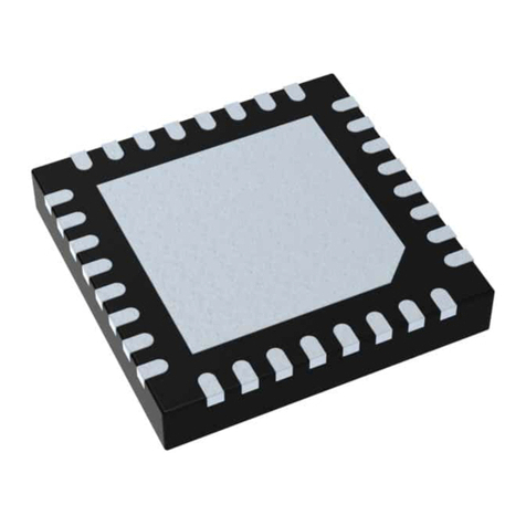
The Si5357 is a high-performance, low-jitter clock generator capable of synthesizing
five independent banks of user-programmable clock frequencies up to 312.5 MHz. The
device supports free run operation using an external crystal, or it can lock to an external
clock signal. The output drivers support up to twelve LVCMOS clocks. Separate output
supply pins allow supply voltages of 3.3, 2.5, 1.8 V and 1.5 V to power the output driv-
ers. The core voltage supply (VDD) accepts 3.3, 2.5,or 1.8 V and is independent from
the output supplies (VDDOs). Using its two-stage synthesis architecture and patented
high-resolution Multisynth technology, the Si5357 can generate three fully independent /
non-harmonically-related bank frequencies from a single input frequency.
÷ P PFD LF
÷Mn/Md
÷R
÷R
÷R
÷R
÷R
÷R
÷N0
÷N1
÷O0
÷O1
÷O2
÷O3
÷O4
1-31
10-255
10-50 MHz 2.375-2.625 GHz
10-255
8-255
10-170 MHz
10-170 MHz
10-170 MHz
10-170 MHz
10-170 MHz
10-170 MHz
10-170 MHz
1-63
10-50 MHz
10-170 MHz
10-170 MHz
10-30 MHz
VDD_XTAL
VDDA
VDDOA
VDDOB
VDDOC
VDDOD
VDDOE
XA/CLKIN_1
XB
CLKIN_2
nCLKIN_2
OUT0
OUT1
OUT2
OUT3
OUT4
OUT5
OUT6
OUT7
OUT8
OUT9
OUT10
OUT11
KEY FEATURES
• Any-Frequency 12-output programmable
clock generator
• Offered in 32-pin QFN package
• Multisynth technology enables any
frequency synthesis on any output up to
170 MHz
• Highly configurable output path featuring a
cross point mux
• Up to three independent fractional
synthesis output paths
• Up to five independent integer dividers
• Embedded 50 MHz crystal option
• Input frequency range:
• External crystal: 16 to 50 MHz
• Differential clock: 10 to 170 MHz
• LVCMOS clock: 10 to 170 MHz
• Output frequency range:
• LVCMOS: 5 to 170 MHz
• Temperature range: –40 to +85 °C
• Pb-free, RoHS-6 compliant
• For more information, refer to the Si5357
data sheet
Skyworks Solutions, Inc. • Phone [781] 376-3000 • Fax [781] 376-3100 • [email protected] • www.skyworksinc.com
1Rev. 0.2 • Skyworks Proprietary Information • Products and Product Information are Subject to Change Without Notice • July 26, 2021 1

Table of Contents
1. Overview .................................3
2. Power Supply Sequencing ..........................4
3. Input Clocks................................5
3.1 Input Clock Terminations ..........................6
3.2 Crystal Recommendations .........................9
4. GPI .................................. 10
5. Output Clock Terminations ..........................11
5.1 DC-Coupled Output Clock Terminations .....................12
6. Programming the Volatile Memory ...................... 13
6.1 Programming the PLL ...........................14
6.2 Programming the Clock Path .........................17
6.3 Programming the Output Clock Frequency ....................18
6.4 Programming the Output Clock Format ......................19
6.5 Programming for Frequency Select Operations ...................20
6.6 Programming for Spread Spectrum .......................21
7. Recommended Schematic and Layout Practices ................. 23
8. Register Map .............................. 24
Skyworks Solutions, Inc. • Phone [781] 376-3000 • Fax [781] 376-3100 • [email protected] • www.skyworksinc.com
2Rev. 0.2 • Skyworks Proprietary Information • Products and Product Information are Subject to Change Without Notice • July 26, 2021 2

1. Overview
In addition to clock generation, the inputs can bypass the synthesis stage enabling the Si5357 to be used as a high-performance clock
buffer or a combination of a buffer and generator. For applications that need fine frequency adjustments, such as clock margining,
outputs from the MultiSynth bank can be incremented or decremented by at least ±50 ppm in user-defined steps as low as 10-20 ppb
per step. This can be done through ID frequency select feature. Spread spectrum is available for any clock output from two Multisynth
dividers for use in EMI-sensitive applications, such as PCI Express. Configurations and controls of the Si5357 are mainly handled
through I2C. Any GPI pin can be programmed to be clock input select, frequency select, spread enable, output enable, resetb, and I2C
address select.
To enable in-system programming, a power up mode is available through OTP which powers up the chip in an OTP defined default
mode but with no outputs enabled. This allows a microcontroller to first write a user defined subset of the registers and then restart the
power-up sequence to activate the newly programmed configuration without re-downloading the OTP.
Si5357 Reference Manual • Overview
Skyworks Solutions, Inc. • Phone [781] 376-3000 • Fax [781] 376-3100 • [email protected] • www.skyworksinc.com
3Rev. 0.2 • Skyworks Proprietary Information • Products and Product Information are Subject to Change Without Notice • July 26, 2021 3

2. Power Supply Sequencing
The Si5357 VDD_core voltages are VDD_DIG, VDD_XTAL and VDDA. These 3 VDD_core pins must all use the *same* voltage.
Power supply sequencing between VDD_core and any VDDOx pin is allowed in any order. However, to minimize the “bring up” time,
it is recommended that VDD_core is powered up first, this ensures that the NVM download is completed first. The register bit field
“VDD_XTAL_OK” is set to indicate input buffer(s) and crystal oscillator are powered up. Once the appropriate VDDOx supplies are
powered-up, the VDDO_OK register field will indicate output driver bank supply voltage status. These status registers are available
to provide an indication of general device status and presence of output driver voltages. The figure below shows the Si5332 device
power-up sequencing and expected device behavior. Note that a blank (unconfigured) part will stop and wait to be configured with
outputs disabled.
Power supplies for VDDA,
VDD_DIG, VDD_XTAL
stable
Time (system time delay)
for NVM download
Is this a blank part?
Yes
No
Time (system time delay) for
Oscillator startup/ Time
(system time delay) for input
clock availability
Time (system time delay)
for PLL lock
Outputs available and
stable
Program Si5332 volatile
memory with a frequency
plan
Figure 2.1. Power Supply Sequencing for Si5357
Si5357 Reference Manual • Power Supply Sequencing
Skyworks Solutions, Inc. • Phone [781] 376-3000 • Fax [781] 376-3100 • [email protected] • www.skyworksinc.com
4Rev. 0.2 • Skyworks Proprietary Information • Products and Product Information are Subject to Change Without Notice • July 26, 2021 4

3. Input Clocks
The Si5357 has three input clock nodes, the XA/XB pair, the CLKIN_2/CLKIN_2# pair and the CLKIN_3/CLKIN_3# pair.
XA/XB supports a crystal input or an external clock input whereas the CLKIN_x/CLKIN_x# pairs support ONLY external clock inputs.
The GPI pins can be set to select the active input clock for the PLL (or the user can set the active input via register writes).
Si5357 Reference Manual • Input Clocks
Skyworks Solutions, Inc. • Phone [781] 376-3000 • Fax [781] 376-3100 • [email protected] • www.skyworksinc.com
5Rev. 0.2 • Skyworks Proprietary Information • Products and Product Information are Subject to Change Without Notice • July 26, 2021 5

3.1 Input Clock Terminations
The crystal oscillator supports 16-50 MHz crystals and supports internal crystal loads. When external input clocks can only be AC-cou-
pled into the XA/XB input. The CLKIN_x/CLKIN_x# can accept either a DC-coupled CMOS input clock or AC-coupled CMOS/differential
clocks. The recommended terminations are shown in the figures below.
XA
XB
Clock IC
Figure 3.1. Termination for Connecting a Crystal to XA/XB Pins in "Crystal" Mode
XA
XB
Clock IC
External oscillator/clock source
0.1 µF
0.1 µF
Input buffer
Limit swing at the input to
less than 1V
Add any output termination
needed by the external
oscillator/clock source
before the 0.1 µF
capacitances
Figure 3.2. Termination for Connecting an External Clock Input to XA/XB Pins
Key differences between Figure 3.1 Termination for Connecting a Crystal to XA/XB Pins in "Crystal" Mode on page 6 and Figure
3.2 Termination for Connecting an External Clock Input to XA/XB Pins on page 6 are:
1. Termination for a reference clock input on XA/XB must be external to Si5357.
2. The choice to enable the internal crystal oscillator or internal capacitance loads or to disable their use is controlled by programming
the Si5357 by setting the right user registers (refer to the in this reference manual or to the ClockBuilder Pro).
Because of the above differences, it is not possible to use these two modes interchangeably without modifications to terminations and
internal register re-programming of the Si5357.
Si5357 Reference Manual • Input Clocks
Skyworks Solutions, Inc. • Phone [781] 376-3000 • Fax [781] 376-3100 • [email protected] • www.skyworksinc.com
6Rev. 0.2 • Skyworks Proprietary Information • Products and Product Information are Subject to Change Without Notice • July 26, 2021 6

CLKIN_x
CLKIN_x#
Clock IC
External oscillator/clock source
0.1 µF
0.1 µF
Input buffer
Add any output termination
needed by the external
oscillator/clock source
before the 0.1 µF
capacitances
Figure 3.3. Termination for AC-Coupling a Differential Clock Input to CLKIN _x/CLKIN_x# Pins
CLKIN_x
CLKIN_x#
Clock IC
External oscillator/clock source
Input buffer
100 ohms
Figure 3.4. Termination for AC-Coupling an External LVDS Clock Input to CLKIN_x/CLKIN_x# Pins
CLKIN_x
CLKIN_x#
Clock IC
External oscillator/clock source
Input buffer
Add any output termination
needed by the clock source
Figure 3.5. Termination for DC-Coupling a Differential Clock Input to CLKIN_x/CLKIN_x# Pins
Si5357 Reference Manual • Input Clocks
Skyworks Solutions, Inc. • Phone [781] 376-3000 • Fax [781] 376-3100 • [email protected] • www.skyworksinc.com
7Rev. 0.2 • Skyworks Proprietary Information • Products and Product Information are Subject to Change Without Notice • July 26, 2021 7

CLKIN_x
CLKIN_x#
Clock IC
External oscillator/clock source
Input buffer
100 ohms
Figure 3.6. Termination for DC-Coupling an External LVDS Clock Input to CLKIN_x/CLKIN_x# Pins
CLKIN_x
CLKIN_x#
Clock IC
External oscillator/clock source
Input buffer
0.1 µF
The swing of the
clock source
should match the
VDD CORE value
Figure 3.7. Termination for DC-Coupling a Single-Ended Clock Input to CLKIN_x/CLKIN_x# Pins
CLKIN_x
CLKIN_x#
Clock IC
External oscillator/clock source
Input buffer
0.1 µF
The swing of the
clock source can
be any value
between 1V – 4V
0.1 µF
Figure 3.8. Termination for AC-Coupling a Single-Ended Clock Input to CLKIN_x/CLKIN_x# Pins
Si5357 Reference Manual • Input Clocks
Skyworks Solutions, Inc. • Phone [781] 376-3000 • Fax [781] 376-3100 • [email protected] • www.skyworksinc.com
8Rev. 0.2 • Skyworks Proprietary Information • Products and Product Information are Subject to Change Without Notice • July 26, 2021 8

3.2 Crystal Recommendations
The crystals in the table below are recommended for use with Si5357. The crystals listed are 25 and 27 MHz frequencies. However,
when choosing any crystal frequency between 16-30 MHz, a crystal with with ESR less than (or equal to) 50 Ω and CL less than (or
equal to) 20 pF can be used with Si5357. When choosing crystals of 31-50 MHz frequencies, C0 should not exceed 2 pF, CL should not
exceed 10 pF and the ESR should not exceed 50 Ω.
Table 3.1. Recommended Crystals
Crystal Part Number Make Stability CL ESR
ECS-25-18-30B-AKN ECS 30ppm 18pf 30 Ω
ECS-27-18-30B-AKN 30ppm 18pf 30 Ω
FOXSDLF/250FR-20 Fox 30ppm 20pf 30 Ω
FA-238V-25.000000MHz12.0+15.0-15.0 Epson 50ppm 12pf 50 Ω
ABM3B-25.000MHz-18-50-D1U Abracon 20ppm 18pf 50 Ω
ABM3B-27.000MHz-18-50-D1U 20ppm 18pf 50 Ω
ABM3B-25.000MHz-18-60-D1U 30ppm 18pf 60 Ω
ABM3B-27.000MHz-18-60-D1U 30ppm 18pf 60 Ω
ABM3B-25.000MHz-12-50-D1U 10ppm 10pf 50 Ω
ABM3B-27.000MHz-12-50-D1U 10ppm 10pf 50 Ω
AA-25.000MALE-T TXC 30ppm 12pf 50 Ω
AA-27.000MAGK-T 30ppm 20pf 50 Ω
FQ5032B-25.000 Fox 30ppm 20pf 50 Ω
FQ5032B-27.000
NX5032GA-25.000M-STD-CSK-4 NDK 30ppm 8pf 50 Ω
NX5032GA-25.000000MHZ-LN-CD-1 30ppm 8pf 70 Ω
NX5032GA-27M-STD-CSK-4 30ppm 8pf 50 Ω
NX5032GA-27.000000MHZ-LN-CD-1 30ppm 8pf 70 Ω
7A-25.000MAAE TXC 30ppm 12pf 50 Ω
7A-25.000MAAJ 30ppm 18pf 50 Ω
7A-27.000MAAE 30ppm 12pf 50 Ω
7A-27.000MAAJ 30ppm 18pf 50 Ω
When a crystal input is used, it is strongly recommended that the internal load capacitances (CL in table 1) are enabled. CL is the total
capacitance load across the XA, XB nodes. Therefore, the individual capacitances on each node need to be 2*CL. The method to set
the CL is as follows:
1. Enable internal CL loading by setting the XOSC_CINT_ENA bit field.
2. The load on each node, (XA and XB), is set by writing to the register fields XOSC_CTRIM_XA, XOSC_CTRIM_XB re-spectively
using the equation below:
2 ×
CL
= 10
pF
+ 0.5
pF
×
XOSC
_
CTRIM
_
XA
(
XOSC
_
CTRIM
_
XA
=
XOSC
_
CTRIM
_
XB
)
Using internal CL is recommended because it:
• Reduces the interference from the crystal oscillation into the Si5357 PLL system and therefore keeps the phase noise at an optimal
performance level.
• Reduces PCB area.
Si5357 Reference Manual • Input Clocks
Skyworks Solutions, Inc. • Phone [781] 376-3000 • Fax [781] 376-3100 • [email protected] • www.skyworksinc.com
9Rev. 0.2 • Skyworks Proprietary Information • Products and Product Information are Subject to Change Without Notice • July 26, 2021 9

4. GPI
The General-purpose inputs (GPI pins) are pins whose input functions can be programmed (in NVM) to assume a pre-defined function.
The Si5357 provides users the following options for each GPI pin available for programming.
A general-purpose input can be programed as one of the following pins:
Table 4.1. GPI Programming Guide
Function Name Description
OE_0 Output enable input for OUT0
OE_1 Output enable input for OUT1
OE_2 Output enable input for OUT2
OE_3 Output enable input for OUT3
OE_4 Output enable input for OUT4
OE_5 Output enable input for OUT5
OE_6 Output enable input for OUT6
OE_7 Output enable input for OUT7
OE_8 Output enable input for OUT8
OE_9 Output enable input for OUT9
OE_10 Output enable input for OUT10
OE_11 Output enable input for OUT11
SSE_0 Spread spectrum control for outputs derived from N0
SSE_1 Spread spectrum control for outputs derived from N1
FS_N0 Frequency select for outputs derived from N0
FS_N1 Frequency select for outputs derived from N1
FS_O0 Frequency select for outputs derived from O0
FS_O1 Frequency select for outputs derived from O1
FS_O2 Frequency select for outputs derived from O2
FS_O3 Frequency select for outputs derived from O3
FS_O4 Frequency select for outputs derived from O4
CLKIN_SEL0 Input clock select (LSB)
CLKIN_SEL1 Input clock select (MSB)
I2C_ADDR Selection control for i2c address
ClockBuilder Pro will allow a user to select similar functions to choose a single GPI input. For instance, FS_x functions will be allowed
to share a single GPI pin but a FS_x function and OE_y function will not be allowed to share a single GPI input.
The default I2C address for Si5357 is 6B. This I2C address can be customized and the user can select between “two” different I2C
addresses using the I2C_ADDR function.
GPI pin functionality is only available when creating customized Si5357 configuration files and part numbers through ClockBuilder Pro.
GPI function assignment and definition is not available through I2C programming, meaning GPI pin use is not available in base parts.
Si5357 Reference Manual • GPI
Skyworks Solutions, Inc. • Phone [781] 376-3000 • Fax [781] 376-3100 • [email protected] • www.skyworksinc.com
10 Rev. 0.2 • Skyworks Proprietary Information • Products and Product Information are Subject to Change Without Notice • July 26, 2021 10

5. Output Clock Terminations
The Si5357 output formats are programable and cover all popular output formats. The output drivers can be set by the programming the
following bit fields:
Table 5.1. Output Format Related Register Fields
outx_mode: - Sets the mode of the driver.
outx_cmos_inv: - Sets an inverted copy for CMOS driver format.
outx_cmos_slew: - Sets the slew rate of the CMOS driver.
outx_cmos_str: - Sets the output impedance of the CMOS driver.
Table 5.2. OUTx_Mode vs Output Formats
OUTx_MODE Driver Mode
0 off
1 CMOS on positive output only
2 CMOS on negative output only
3 dual CMOS outputs
The recommended termination for each output format is shown in figures below.
Si5357 Reference Manual • Output Clock Terminations
Skyworks Solutions, Inc. • Phone [781] 376-3000 • Fax [781] 376-3100 • [email protected] • www.skyworksinc.com
11 Rev. 0.2 • Skyworks Proprietary Information • Products and Product Information are Subject to Change Without Notice • July 26, 2021 11

5.1 DC-Coupled Output Clock Terminations
1.425V to 3.63V
OUTx
OUTx
Zo=50Ω
Zo=50Ω
Set output driver
to 50Ω mode.
Figure 5.1. LVCMOS Termination, Option 1
1.425 to 3.63V
OUTx
Rs
OUTx
Zo=50Ω
Zo=50Ω
Rs
Rs = Zo – Rdrv
Set output driver
to 25Ω mode.
Figure 5.2. LVCMOS Termination, Option 2
Si5357 Reference Manual • Output Clock Terminations
Skyworks Solutions, Inc. • Phone [781] 376-3000 • Fax [781] 376-3100 • [email protected] • www.skyworksinc.com
12 Rev. 0.2 • Skyworks Proprietary Information • Products and Product Information are Subject to Change Without Notice • July 26, 2021 12

6. Programming the Volatile Memory
The volatile memory can be programmed to set up the various functions necessary to realize a PLL function, a clock output to clock
input relationship and can be used to monitor input clock that controls the PLL. The front-page block diagram is repeated here to
refresh the various limits and possibilities that are necessary for the calculations below.
÷ P PFD LF
÷Mn/Md
÷R
÷R
÷R
÷R
÷R
÷R
VDD_XTAL
VDDA
VDDOA
VDDOB
VDDOC
VDDOD
VDDOE
XA/CLKIN_1
XB
CLKIN_2
nCLKIN_2
OUT0
OUT1
OUT2
OUT3
OUT4
OUT5
OUT6
OUT7
OUT8
OUT9
OUT10
OUT11
÷N0b
÷N0a
÷N1b
÷N1a
÷O0b
÷O0a
÷O1b
÷O1a
÷O2b
÷O2a
÷O3b
÷O3a
÷O4b
÷O4a
Figure 6.1. Top Level Block Diagram
Si5357 Reference Manual • Programming the Volatile Memory
Skyworks Solutions, Inc. • Phone [781] 376-3000 • Fax [781] 376-3100 • [email protected] • www.skyworksinc.com
13 Rev. 0.2 • Skyworks Proprietary Information • Products and Product Information are Subject to Change Without Notice • July 26, 2021 13

6.1 Programming the PLL
The PLL programming involves three distinct constraints:
1. The minimum and the maximum frequencies possible for the PFD (Phase Frequency Detector) at lock. That is set by the reference
frequency which is set the input divider P and the active input clock as selected by the IN SEL pins or registers.
2. The VCO frequency that is set by feedback divider (Mn/Md) and the PFD frequency also has a limited range that is unique to
Si5357.
3. The PLL closed loop transfer function characterized by its loop band width and peaking is set by programming the loop parame-
ters.
The table below lists the constraints for the PLL reference frequency and the VCO frequency. The PLL reference frequency
(pllRefFreq) and the VCO frequency (vcoFreq) are related by the equation below:
vcoFreq
=
pllRefFreq
× (
Mn
Md
)
For a given plan, the pllRefFreq can be readily solved as it is derived from the input clock frequency. The first step in this optimization
should be to derive a pllRefFreq that is within the 10-50 MHz limit. To get to this optimization, the “active” input to the PLL must be
selected from the XA/XB, CLKIN_1 input clocks using either the IMUX_SEL register field or the CLKIN_SEL pins {if CLKIN_SEL pins
are available in the custom part that you choose to re-program}. PllRefFreq is given by the InFreq (active clock input frequency) and P
as:
PllRefFreq
=
InFreq
P
Table 6.1. Constraints for PLL Reference Frequency and VCO Frequency
Field Name Value Description
pllMinRefFreq 10 MHz The minimum reference frequency the PLL
can tolerate
pllMaxRefFreq 50 MHz The maximum reference frequency the PLL
can tolerate
vcoCenterFreq 2.5 GHz The center frequency of the VCO’s tuning
range
vcoMinFreq 2.375 GHz The minimum frequency of the VCO’s tun-
ing range
vcoMaxFreq 2.625 GHz The maximum frequency of the VCO’s tun-
ing range
List all required output frequencies, Fx, where x = 0,1,2,3,4,5. Note that there are only “six” unique frequencies possible in the Si5357
(even though there are 12 outputs. An output pair, OUT2X, OUT2X+1 have frequency Fx) and is shown in Table5. The integer
O-dividers are denoted by hsdiv. Each Oi divider maps to a hsdivi in the solver where i is an integer between 0 and 4. Similarly, the two
Multisynth N-dividers, Nj map to IDj and j = 0 or 1.The constraints for these divider values are listed in the table below.
Si5357 Reference Manual • Programming the Volatile Memory
Skyworks Solutions, Inc. • Phone [781] 376-3000 • Fax [781] 376-3100 • [email protected] • www.skyworksinc.com
14 Rev. 0.2 • Skyworks Proprietary Information • Products and Product Information are Subject to Change Without Notice • July 26, 2021 14

Table 6.2. Output Frequency Variables Grouping and Mapping to Actual Output Pins
Si5357 Output Output Frequency Variable for Solver
OUT0, OUT1 F0
OUT2, OUT3 F1
OUT4, OUT5 F2
OUT6, OUT7 F3
OUT8, OUT9 F4
OUT10, OUT11 F5
Table 6.3. Constraints for hsdiv and id
Field Name Value Description
hsdivMinDiv 8 The minimum divide value that the HSDIV
can support
hsdivMaxDiv 255 The maximum divide value that the HSDIV
can support
idMinDiv 10 The minimum divide value that the ID can
support
idMaxDiv 255 The maximum divide value that the ID can
support
Each output frequency Foutxy is given by:
Foutxy
=
vcoFreq
{
hsdivj
×
Rxy
}
or
Foutxy
=
vcoFreq
{
idj
×
Rxy
}
Given these constraints, the solve must first choose a VCO frequency that is satisfies the constraints in Table 3. The search for
VcoFreq can be broken down into the following steps.
1. From the output frequency set, form a set of “M” non-equal frequencies. Derive the (N-M) equal frequencies from the same divider
idj or hsdivi.
2. Now form MC2 groups of {M-2} output frequencies. Find the LCM of each group and find an integer “I” that can such that:
a. vcoFreq = I*LCM can meet the constraint for vcoFreq in Table 6.1 Constraints for PLL Reference Frequency and VCO
Frequency on page 14.
b. List the “L” groups that provide a legal vcoFreq, i.e., a vcoFreq that satisfies the condition in step a.
c. Choose the vcoFreq that has most number of performance critical clocks that do not need “spread spectrum” clock-ing as part
of the “M-2” output clocks.
Given that vcoFreq, calculate the feedback divider as:
Mn
Md
=
vcoFreq
pllRefFreq
The Mn/Md fraction is represented in register fields IDPA_INTG, IDPA_RES and IDPA_DEN
IDPA
_
INTG
=
floor
(128 ×
vcoFreq
pllRefFreq
)
IDPA
_
RES
IDPA
_
DEN
=128 ×
vcoFreq
pllRefFreq
-
IDPA
_
INTG
As can be seen from the above equations, the ratio IDPA_RES/ IDPA_DEN will always be less than 1.
Si5357 Reference Manual • Programming the Volatile Memory
Skyworks Solutions, Inc. • Phone [781] 376-3000 • Fax [781] 376-3100 • [email protected] • www.skyworksinc.com
15 Rev. 0.2 • Skyworks Proprietary Information • Products and Product Information are Subject to Change Without Notice • July 26, 2021 15

Note: All these register fields are 15 bits wide. Therefore, the fraction will need to truncate to up to this precision. This section fully
determines the VCO frequency, the P-divider and the feedback divider for this plan given the choice of using O-dividers {HSDIV} for
M-2 output clocks and N-dividers {ID} for two output clocks.
The next step will be to determine the closed loop response that is required from the PLL. The table below lists the different loop BW
settings possible and the register field value that will enable that loop BW setting:
Table 6.4. Loop BW Options
PLL_MODE Loop Bandwidth (kHz) PLL. Ref. Freq. Min (MHz) PLL. Ref. Freq. Max. (MHz)
0 ILLEGAL IF PLL MODE IS ENABLED
1 350 10 15
2 250 10 15
3 175 10 15
4 500 15 30
5 350 15 30
6 250 15 30
7 175 15 30
8 500 30 50
9 350 30 50
10 250 30 50
11 175 30 50
This algorithm will result in a final solution for a VCO frequency, vcoFreq, that can then be used to calculate the O-divider , N-divider,
and R-divider values needed to derive each output frequency, Fx.
Si5357 Reference Manual • Programming the Volatile Memory
Skyworks Solutions, Inc. • Phone [781] 376-3000 • Fax [781] 376-3100 • [email protected] • www.skyworksinc.com
16 Rev. 0.2 • Skyworks Proprietary Information • Products and Product Information are Subject to Change Without Notice • July 26, 2021 16

6.2 Programming the Clock Path
Given a valid VCO frequency for the M unique frequencies, segregate the N-M equal frequencies into known output banks. When
arranging outputs, care must be taken to minimize crosstalk (without violating the constraints imposed from the grouping of output
frequencies into the VDDO “banks”). Whenever several high frequencies, fast rise time, large amplitude signals are all close to one
another, the laws of physics dictate that there will be some amount of crosstalk. The jitter of the Si5357 is low and therefore crosstalk
can become a significant portion of the final measured output jitter. Some of the source of the crosstalk will be the Si5357 and some will
be introduced by the PCB. For extra fine tuning and optimization in addition to following the usual PCB layout guidelines, crosstalk can
be minimized by modifying the arrangements of different output clocks
A few guidelines are:
1. Avoid adjacent frequency values that are close. A 155.52 MHz clock should not be next to a 156.25 MHz clock. If the jitter
integration bandwidth goes up to 20 MHz, then keep adjacent frequencies at least 20 MHz apart.
2. Adjacent frequency values that are integer multiples of one another are okay and these outputs should be grouped accordingly.
3. Unused outputs can be used to separate clock outputs that might otherwise interfere with one another. If some outputs have tight
jitter requirements while others are relatively loose, rearrange the clock outputs so that the critical outputs are the least susceptible
to crosstalk. These guidelines typically only need to be followed by those applications that wish to achieve the highest possible
levels of jitter performance. Because CMOS outputs have large pk-pk swings and do not present a balanced load to the VDDO
supplies, Si5357 will have larger jitter than the Si5332.
An output multiplexer (output mux) or crosspoint mux needs to be programmed such that each frequency Fx is set to the correct
O-divider,N-divider, or input clock (in the case of buffering). Each output, Fx, has this common divider or input clock reference that
needs to be set. The multiplier setting that routes the correct divider/clock source to the correct group is shown in the following table.
Table 6.5. Output Mux (Crosspoint Mux) Settings
Register field Description
Omuxx_y_sel0 Selects output mux clock for output clocks OUTx, OUTy:
0 = PLL reference clock before pre-scaler
1 = PLL reference clock after pre-scaler
2 = Clock from CLKIN_2
omuxx_y_sel1 Selects output mux clock for output clocks OUTx, OUTy:
clock source:
0 = HSDIV0
1 = HSDIV1
2 = HSDIV2
3 = HSDIV3
4 = HSDIV4
5 = ID0
6 = ID1
7 = Clock from omuxx_y_sel0
Si5357 Reference Manual • Programming the Volatile Memory
Skyworks Solutions, Inc. • Phone [781] 376-3000 • Fax [781] 376-3100 • [email protected] • www.skyworksinc.com
17 Rev. 0.2 • Skyworks Proprietary Information • Products and Product Information are Subject to Change Without Notice • July 26, 2021 17

The final steps will be to program the hsdiv and id dividers. The equations below show the relationship between hsdiv, id divider
values with their associated output frequency. They also show the register fields that need to be programmed to set up the divider
values correctly. The register field and the divider value are both denoted by:
hsdivxa
_
div
=
vcoFrq
Foutxa
×
Rxa
The id dividers are calculated as below:
idxa
=
vcoFrq
Foutxa
×
Rxa
The ida fraction is represented in register fields IDPA_INTG, IDPA_RES and IDPA_DEN
IDxA
_
INTG
=
floor
(128 ×
vcoFreq
Foutxa
×
Rxa
)
IDxA
_
RES
IDxA
_
DEN
=128 ×
vcoFreq
Foutxa
×
Rxa
-
IDxA
_
INTG
6.3 Programming the Output Clock Frequency
The Rx_y register fields are programmed as shown in the table below. This last step completes the settings of all dividers that will result
in the frequency plan. When a valid divider solution space cannot be determined, that frequency plan is not realizable in the Si5357.
Table 6.6. Rxy to Register Field Mapping
Divider Value Register Field Description
R0_1 OUT0_1_DIV Driver divider ratio.
0 = disabled
1–63 = divide value
R2_3 OUT2_3_DIV Driver divider ratio.
0 = disabled
1–63 = divide value
R4_5 OUT4_5_DIV Driver divider ratio.
0 = disabled
1–63 = divide value
R6_7 OUT6_7_DIV Driver divider ratio.
0 = disabled
1–63 = divide value
R8_9 OUT8_9_DIV Driver divider ratio.
0 = disabled
1–63 = divide value
R10_11 OUT10_11_DIV Driver divider ratio.
0 = disabled
1–63 = divide value
Si5357 Reference Manual • Programming the Volatile Memory
Skyworks Solutions, Inc. • Phone [781] 376-3000 • Fax [781] 376-3100 • [email protected] • www.skyworksinc.com
18 Rev. 0.2 • Skyworks Proprietary Information • Products and Product Information are Subject to Change Without Notice • July 26, 2021 18

6.4 Programming the Output Clock Format
The following tables provide the method to fully define every driver.
Table 6.7. Driver Set Up Options
Driver Register Field Description
Driver for output OUTx OUTx_mode Software interpreted driver configuration.
See Table 6.8 Driver Mode Options on
page 19.
OUTx _skew Skew control. Applies to both pad_p and
pad_m. Decoded as unsigned integer with
35 ps / step.
OUTx _stop_highz Driver output state when stopped.
0 = low-z
1 = high-z
OUTx _cmos_inv Sets the polarity of the two outputs.
0 = clk_p
1 = clk_m
OUTx _cmos_slew Controls CMOS slew rate from fast to slow.
00 = fastest
01 = slow
10 = slower
11 = slowest
OUTx _cmos_str CMOS output impedance control.
0 = 50 Ω
1 = 25 Ω
Table 6.8. Driver Mode Options
drvxy_MODE Driver Mode
0 off
1 CMOS on positive output only
2 CMOS on negative output only
Si5357 Reference Manual • Programming the Volatile Memory
Skyworks Solutions, Inc. • Phone [781] 376-3000 • Fax [781] 376-3100 • [email protected] • www.skyworksinc.com
19 Rev. 0.2 • Skyworks Proprietary Information • Products and Product Information are Subject to Change Without Notice • July 26, 2021 19

6.5 Programming for Frequency Select Operations
Every hsdiv and id has a Bank A and a Bank B divider. The register field names that begin with hsdivxb or idxb denote Bank B
dividers. Any FS frequency will be:
FoutxyFS
=
vcoFreq
idxb
Or
FoutxyFS
=
vcoFreq
hsdivb
Any output associated with either idxa or hsdivxa can be switched into the above FS frequency. The control that selects the Bank B
divider is as shown in table below.
Table 6.9. The Control Register Bit to Switch Frequencies
Register Field Description
hsdivx_div_sel Selects bank A or bank B divider HSDIVx settings. The HSDIVx
supports dynamic integer divider changes through this divider se-
lect control bit.
0 = bank A divider
1 = bank B divider
idx_cfg_sel Output divider IDx configuration bank select. The interpolative di-
vider supports dynamically switching between two complete con-
figurations controlled by this bit. Reconfiguration should be done
on the unselected bank. If IDx_CFG=0, running based off bank
A, then bank B may be freely reconfigured and once ready all
changes will be applied to the ID once IDx_CFG=1 thus changing
the ID from bank A to bank B. Spread spectrum enable fields
IDxA_SS_ENA and IDxB_SS_ENA are the only exception and
may be enabled/disabled while bank is selected.
0 = bank A
1 = bank B
In a factory-programmed part, a pin (the FS pin) can be used for the same purpose as the control registers. Once, a control bit is set,
the backup divider values control the output frequency and that is described the equations below:
O-Divider
hsdivxb
_
div
=
vcoFreq
Foutxb
×
Rxa
N-Divider
idxb
=
vcoFreq
Foutxb
×
Rxa
The ida fraction is represented in register fields IDPB_INTG, IDPB_RES and IDPB_DEN
IDxB
_
INTG
=
floor
(128 ×
vcoFreq
Foutxb
×
Rxa
)
IDxB
_
RES
IDxB
_
DEN
=128 ×
vcoFreq
Foutxb
×
Rxa
-
IDxB
_
INTG
As can be seen, the backup divider values limit the possible values for the output frequency in this backup mode. Another key feature
is that the switch to a FS frequency is “glitchless”. Therefore, the recommended method for glitchless frequency updates is to program
either divider a or b (when divider b or a is currently driving the output frequency), and then switch this divider.
Si5357 Reference Manual • Programming the Volatile Memory
Skyworks Solutions, Inc. • Phone [781] 376-3000 • Fax [781] 376-3100 • [email protected] • www.skyworksinc.com
20 Rev. 0.2 • Skyworks Proprietary Information • Products and Product Information are Subject to Change Without Notice • July 26, 2021 20
Table of contents
Other Skyworks Clock manuals
