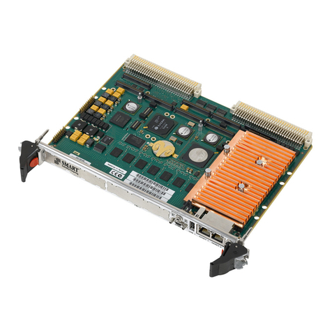
SMART Embedded Computing MVME7100ET User manual

MVME7100ET Single Board Computer
Programmer’s Reference
P/N: 6806800K88C
October 2019

© 2019 SMART Embedded Computing™, Inc.
All Rights Reserved.
Trademarks
The stylized "S" and "SMART" is a registered trademark of SMART Modular Technologies, Inc. and “SMART Embedded
Computing” and the SMART Embedded Computing logo are trademarks of SMART Modular Technologies, Inc. All other names
and logos referred to are trade names, trademarks, or registered trademarks of their respective owners. These materials are
provided by SMART Embedded Computing as a service to its customers and may be used for informational purposes only.
Disclaimer*
SMART Embedded Computing (SMART EC) assumes no responsibility for errors or omissions in these materials. These
materials are provided "AS IS" without warranty of any kind, either expressed or implied, including but not limited to,
the implied warranties of merchantability, fitness for a particular purpose, or non-infringement. SMART EC further does
not warrant the accuracy or completeness of the information, text, graphics, links or other items contained within these
materials. SMART EC shall not be liable for any special, indirect, incidental, or consequential damages, including without
limitation, lost revenues or lost profits, which may result from the use of these materials. SMART EC may make changes to
these materials, or to the products described therein, at any time without notice. SMART EC makes no commitment to update
the information contained within these materials.
Electronic versions of this material may be read online, downloaded for personal use, or referenced in another document as a
URL to a SMART EC website. The text itself may not be published commercially in print or electronic form, edited, translated,
or otherwise altered without the permission of SMART EC.
It is possible that this publication may contain reference to or information about SMART EC products, programming, or services
that are not available in your country. Such references or information must not be construed to mean that SMART EC intends
to announce such SMART EC products, programming, or services in your country.
Limited and Restricted Rights Legend
If the documentation contained herein is supplied, directly or indirectly, to the U.S. Government, the following notice shall apply
unless otherwise agreed to in writing by SMART Embedded Computing.
Use, duplication, or disclosure by the Government is subject to restrictions as set forth in subparagraph (b)(3) of the Rights in
Technical Data clause at DFARS 252.227-7013 (Nov. 1995) and of the Rights in Noncommercial Computer Software and
Documentation clause at DFARS 252.227-7014 (Jun. 1995).
SMART Embedded Computing, Inc.
2900 S. Diablo Way, Suite 190
Tempe, Arizona 85282
USA
*For full legal terms and conditions, visit www.smartembedded.com/ec/legal
Table of Contents
MVME7100ET Single Board Computer Programmer’s Reference (6806800K88C) 3
About this Manual ...............................................................11
1 Introduction.................................................................15
1.1 Overview ...............................................................15
1.2 Ordering and Support Information ...........................................15
1.3 Features ...............................................................16
1.4 Block Diagram ..........................................................19
1.5 Functional Description ....................................................20
1.6 Programming Model ......................................................20
2 MemoryMaps...............................................................21
2.1 Overview ...............................................................21
2.1.1 Default Processor Memory Map........................................21
2.1.2 Suggested Processor Memory Map.....................................21
2.1.3 PCI Memory Map ...................................................22
2.1.4 VME Memory Map ..................................................23
3 Register Descriptions.........................................................25
3.1 Overview ...............................................................25
3.1.1 System Status Register ..............................................28
3.1.2 System Control Register .............................................30
3.1.3 Status Indicator Register .............................................31
3.1.4 NOR Flash Control/Status Register .....................................32
3.1.5 Interrupt Register 1 .................................................33
3.1.6 Interrupt Register 2 .................................................34
3.1.7 Presence Detect Register ............................................35
3.1.8 NAND Flash Chip 1 Control Register....................................36
3.1.9 NAND Flash Chip 1 Select Register ....................................36
3.1.10 NAND Flash Chip 1 Presence Register ..................................37
3.1.11 NAND Flash Chip 1 Status Register ....................................38
3.1.12 NAND Flash Chip 2 Control Register....................................38
3.1.13 NAND Flash Chip 2 Select Register ....................................39
3.1.14 NAND Flash Chip 2 Presence Register ..................................40
3.1.15 NAND Flash Chip 2 Status Register ....................................40
3.1.16 Watch Dog Timer Load Register .......................................41

4 MVME7100ET Single Board Computer Programmer’s Reference (6806800K88C)
Table of Contents
3.1.17 Watch Dog Control Register ..........................................41
3.1.18 Watch Dog Timer Resolution Register...................................42
3.1.19 Watch Dog Timer Count Register ......................................43
3.1.20 PLD Revision Register ...............................................43
3.1.21 PLD Date Code Register .............................................44
3.1.22 Test Register 1.....................................................44
3.1.23 Test Register 2.....................................................45
3.1.24 External Timer Registers .............................................45
3.1.24.1 Prescaler .................................................45
3.1.24.2 Control Registers ...........................................46
3.1.24.3 Compare Register ..........................................47
3.1.24.4 Counter Register ...........................................47
3.1.25 Geographical Address Register ........................................48
4 Programming Details .........................................................49
4.1 Overview ...............................................................49
4.2 MC864xD Reset Configuration ..............................................49
4.3 MC864xD Interrupt Controller ...............................................54
4.4 Local Bus Controller Chip Select Assignments .................................55
4.5 I2C Device Addresses ....................................................55
4.6 User Configuration EEPROM ...............................................56
4.7 VPD EEPRO ............................................................56
4.8 RTM VPD EEPROM ......................................................57
4.9 Ethernet PHY Address ....................................................57
4.10 Flash Memory ...........................................................57
4.11 PCI/PCI-X Configuration ...................................................58
4.11.1 PCI IDSEL and Interrupt Definition .....................................58
4.11.2 PCI Arbitration Assignments ..........................................59
4.12 Other Software Considerations ..............................................60
4.12.1 LBC Timing Parameters..............................................60
4.13 Clock Distribution ........................................................61
4.13.1 System Clock ......................................................62
4.13.2 Real Time Clock Input ...............................................62
4.13.3 Local Bus Controller Clock Divisor......................................62
A Programmable Configuration Data ..............................................63
A.1 Overview ...............................................................63

Table of Contents
MVME7100ET Single Board Computer Programmer’s Reference (6806800K88C) 5
A.2 List of Devices ..........................................................63
A.3 Vital Product Data (VPD) Introduction ........................................64
A.4 How to Read and Modify VPD Information .....................................64
A.5 What Happens if VPD Information is Corrupted .................................64
A.6 How to Fix Corrupted VPD Information .......................................65
A.7 What if Your Board Has the Wrong VPD ......................................65
A.8 How to Fix Wrong VPD Problems ............................................65
A.9 Checksum Guidelines .....................................................65
A.9.1 Vital Product Data CRC Calculation.....................................65
A.9.2 Serial Presence Detect Checksum Calculation ............................67
A.10 VPD Contents for MVME7100ET Boards ......................................68
A.11 SPD Contents for MVME7100ET Boards ......................................77
B Related Documentation .......................................................83
B.1 SMART Embedded Computing Documentation .................................83
B.2 Manufacturers’ Documents .................................................83
B.3 Related Specifications ....................................................85

6 MVME7100ET Single Board Computer Programmer’s Reference (6806800K88C)
Table of Contents

8 MVME7100ET Single Board Computer Programmer’s Reference (6806800K88C)
Table of Contents

List of Tables
MVME7100ET Single Board Computer Programmer’s Reference (6806800K88C) 9
Table 1-1 Features List ........................................................16
Table 2-1 Default Processor Address Map .........................................21
Table 2-2 Suggested Processor Address Map ......................................21
Table2-3 PCIMemoryMap ....................................................22
Table 3-1 System I/O Memory Map ..............................................25
Table 3-2 System Status Register ...............................................28
Table 3-3 System Control Register ...............................................30
Table 3-4 Status Indicator Register ...............................................31
Table 3-5 NOR Flash Control/Status Register ......................................32
Table 3-6 Interrupt Register 1 ...................................................33
Table 3-7 Interrupt Register 2 ...................................................34
Table 3-8 Presence Detect Register ..............................................35
Table 3-9 NAND Flash Chip 1 Control Register .....................................36
Table 3-10 NAND Flash Chip 1 Select Register ......................................36
Table 3-11 NAND Flash Chip 1 Presence Register ...................................37
Table 3-12 NAND Flash Chip 1 Status Register ......................................38
Table 3-13 NAND Flash Chip 2 Control Register .....................................38
Table 3-14 NAND Flash Chip 2 Select Register ......................................39
Table 3-15 NAND Flash Chip 2 Presence Register ...................................40
Table 3-16 NAND Flash Chip 2 Status Register ......................................40
Table 3-17 Watch dog timer Load Register ..........................................41
Table 3-18 Watch Dog Timer Control Register .......................................41
Table 3-19 Watch Dog Timer count Register ........................................42
Table 3-20 Watch Dog Timer Resolution Register ....................................43
Table 3-21 PLD Revision Register ................................................43
Table 3-22 PLD Date Code Register ..............................................44
Table 3-23 Test Register 1 ......................................................44
Table 3-24 Test Register 2 ......................................................45
Table 3-25 Prescaler Register ...................................................45
Table 3-26 Tick Timer Control Registers ............................................46
Table 3-27 Tick Timer Compare Registers ..........................................47
Table 3-28 Tick Timer Counter Register ............................................47
Table 4-1 MC864xD POR Configuration Settings ....................................49
Table 4-2 MC864xD Interrupt Controller ...........................................54
Table 4-3 LBC Chip Select Assignments ..........................................55
Table 4-4 I2C Bus Device Addressing ............................................55
Table 4-5 PHY Types and MII Management Bus Addresses ...........................57

10 MVME7100ET Single Board Computer Programmer’s Reference (6806800K88C)
Table of Contents
Table 4-6 NOR Flash Memory Configurations ......................................57
Table 4-7 NAND Flash Memory Configurations .....................................58
Table 4-8 IDSEL and Interrupt Mapping for PCI Devices ..............................58
Table 4-9 Planar PCI Device Identification .........................................59
Table 4-10 PCI Arbitration Assignments ............................................60
Table 4-11 LBC Timing Parameters ...............................................60
Table 4-12 Clock Assignments ...................................................61
Table 4-13 Clock Frequencies ...................................................62
Table A-1 Programmable Devices ................................................63
Table A-2 On-board Serial EEPROMs ............................................63
Table A-3 Checksum Calculation Example .........................................67
Table A-4 Static VPD Contents ..................................................68
Table A-5 Variable VPD Contents ................................................75
Table A-6 SPD Contents .......................................................77
Table B-1 SMART EC Documentation ............................................83
Table B-2 Manufacturer’s Publications ............................................83
Table B-3 Related Specifications ................................................85

MVME7100ET Single Board Computer Programmer’s Reference (6806800K88C) 11
About this Manual
Overview of Contents
This manual is divided into the following chapters and appendices:
Chapter 1, Introduction on page 15, provides a brief product description and a block
diagram showing the architecture of the MVME7100ET Single Board Computer.
Chapter 2, Memory Maps on page 21, provides information on the memory maps of the
board.
Chapter 3, Register Descriptions on page 25, contains status registers for the system
resources.
Chapter 4, Programming Details on page 49, includes additional programming information
for the MVME7100ET.
Appendix A, Programmable Configuration Data on page 63, provides additional
programming information including IDSEL mapping, interrupt assignments for the
MC864xD interrupt controller, Flash memory, two-wire serial interface addressing, and
other device and system considerations.
Appendix B, Related Documentation on page 83, provides a listing of related SMART
Embedded Computing manuals, vendor documentation, and industry specifications.
Abbreviations
This document uses the following abbreviations:
Acronym Description
ASCII American Standard Code for Information Interchange
CRC Cyclic Redundancy Check
EEPROM Electrically Erasable Programmable Read Only Memory
FRU Field Replaceable Unit
Flash Flash Memory
GB Gigabyte
HEX Hexadecimal
Hz Hertz
IPMI Intelligent Platform Management Interface
MB Megabyte

12 MVME7100ET Single Board Computer Programmer’s Reference (6806800K88C)
About this Manua
l
About this Manual
Conventions
The following table describes the conventions used throughout this manual:
Mfg Manufacturing
SPD Serial Presence Detect
VPD Vital Product Data
Acronym Description
Notation Description
0x00000000 Typical notation for hexadecimal numbers (digits are 0 through F), for
example used for addresses and offsets
0b0000 Same for binary numbers (digits are 0 and 1)
bold Used to emphasize a word
Screen Used for on-screen output and code related elements or commands.
Sample of Programming used in a table (9pt)
Courier + Bold Used to characterize user input and to separate it from system output
Reference Used for references and for table and figure descriptions
File > Exit Notation for selecting a submenu
<text> Notation for variables and keys
[text] Notation for software buttons to click on the screen and parameter
description
... Repeated item for example node 1, node 2, ..., node 12
.
.
.
Omission of information from example/command that is not necessary at
the time
.. Ranges, for example: 0..4 means one of the integers 0,1,2,3, and 4 (used
in registers)
| Logical OR
Indicates a hazardous situation which, if not avoided, could result in death
or serious injury

About this Manual
MVME7100ET Single Board Computer Programmer’s Reference (6806800K88C) 13
Summary of Changes
This manual has been revised and replaces all prior editions.
Indicates a hazardous situation which, if not avoided, may result in minor
or moderate injury
Indicates a property damage message
Indicates a hot surface that could result in moderate or serious injury
Indicates an electrical situation that could result in moderate injury or death
Indicates that when working in an ESD environment care should be taken
to use proper ESD practices
No danger encountered, pay attention to important information
Notation Description
Part Number Publication Date Description
6806800K88C October 2019 Rebrand to SMART Embedded Computing template
6806800K88B June 2014 Re-branded to Artesyn template.
6806800K88A September 2010 First Release

14 MVME7100ET Single Board Computer Programmer’s Reference (6806800K88C)
About this Manua
l
About this Manual

MVME7100ET Single Board Computer Programmer’s Reference (6806800K88C) 15
Chapter 1
Introduction
1.1 Overview
This chapter briefly describes the board level hardware features of the MVME7100ET
Single Board Computer. Refer to the MC864xD Reference Manual listed in Appendix B,
Related Documentation on page 83, for more details and programming information.
1.2 Ordering and Support Information
Refer to the MVME7100 data sheet for a complete list of available variants and
accessories. Refer to Appendix B, Related Documentation on page 83 or consult your local
SMART Embedded Computing sales representative for the availability of other variants.
For technical assistance, documentation, or to report product damage or shortages, contact
your local SMART EC sales representative or visit our web site at
https://www.smartembedded.com/ec/support/.
NOTE: The IPMC712 and IPMC761 I/O modules are not supported on the MVME7100ET
SBC.

16 MVME7100ET Single Board Computer Programmer’s Reference (6806800K88C)
Introduction
Introduction
1.3 Features
The following table provides a summary of the features common to all board variations.
Table 1-1 Features List
Function Features
Processor / Host
Controller / Memory
Controller
One MC864xD Integrated Processor
Two e600 cores with integrated L2
Core frequency of 1.067 or 1.33 GHz
One integrated four channel DMA controller
Two integrated PCIE interfaces
Four integrated 10/100/1000 Ethernet controllers
One integrated DUART
Two integrated I2C controllers
One integrated Programmable Interrupt Controller
One integrated Local Bus Controller
Two integrated DDR2 SDRAM controllers
System Memory Two banks of DDR2 SDRAM with ECC
2GBor4GB
I2C One 8 KB VPD serial EEPROM
Two 64 KB user configuration serial EEPROMs
One Real Time Clock (RTC) with removable battery
Dual temperature senso
Two SPDs for memory
Connection to XMCspan and RTM
NOR Flash 128 MB soldered flash with two alternate 1 MB boot sectors
selectable via hardware switch
H/W switch or S/W bit write protection for entire logical bank
NAND Flash Up to two devices available:
4 GB - 1 device
8 GB - 2 device

Introduction
MVME7100ET Single Board Computer Programmer’s Reference (6806800K88C) 17
NVRAM One 512 KB MRAM extended temperature range
Two 64 KB serial EEPROMs
PCI-E 8X Port to XMC Expansion
8X Port to 5 Port PCI Express switch
I/O One front panel mini DB-9 connector for front I/O: one serial
channel
Two front panel RJ-45 connectors with integrated LEDs for
front I/O: two 10/100/1000 Ethernet channels
PMC site 1 front I/O and rear P2 I/O
PMC site 2 front I/O
Ethernet Four 10/100/1000 MC864xD Ethernet channels:
Two front panel Ethernet connectors
Two channels for rear P2 I/O
Serial Interface One 16550-compatible, 9.6 to 115.2 Kbaud, MC864xD,
asynchronous serial channel: one channel for front panel I/O
One quad UART (QUART) controller to provide four 16550-
compatible, 9.6 to 115.2 Kbaud, asynchronous serial
channels: four channels for rear P2 I/O
Timers Four 32-bit MC864xD timers
Four 32-bit timers in a PLD
Watchdog Timer One watchdog timer in PLD
VME Interface VME64 (ANSI/VITA 1-1994) compliant (3 row backplane 96-
pin VME connector)
VME64 Extensions (ANSI/VITA 1.1-1997) compliant (5 row
backplane 160-pin VME connector)
2eSST (ANSI/VITA 1.5-2003) compliant
Two five-row P1 and P2 backplane connectors
One Tsi148 VMEbus controller
Form Factor Standard 6U VME, one slot
Table 1-1 Features List (continued)
Function Features

18 MVME7100ET Single Board Computer Programmer’s Reference (6806800K88C)
Introduction
Introduction
Miscellaneous One front panel RESET/ABORT switch
Six front panel status indicators:
Two 10/100/1000 Ethernet link/speed and activity (4 total)
Board fail
User S/W controlled LED
Planar status indicators
One standard 16-pin JTAG/COP header
Boundary scan support
Switches for VME geographical addressing in a three-row
backplane
Software Support VxWorks OS support
Linux OS support
Table 1-1 Features List (continued)
Function Features

Introduction
MVME7100ET Single Board Computer Programmer’s Reference (6806800K88C) 19
1.4 Block Diagram
The following figure is a block diagram of the MVME7100ET architecture.
Figure 1-1 Block Diagram

20 MVME7100ET Single Board Computer Programmer’s Reference (6806800K88C)
Introduction
Introduction
1.5 Functional Description
The MVME7100ET is a VMEbus board based on the MC8640D and MC8641D Integrated
Processors. The MVME7100ET provides 2eSST VMEbus interfaces, dual 64-bit/100MHz
PMC sites, 128MB of NOR flash and up to 8GB of NAND flash, up to 4GB of DDR2
SDRAM, quad 10/100/1000 Ethernet, and five serial ports. The MVME7100ET supports
front and rear I/O with access to the rear I/O via the MVME7100ET transition module.
The MVME7100ET provides front panel access to one serial port with a mini DB-9
connector and two 10/100/1000 Ethernet ports with two RJ-45 connectors. The front panel
includes a fail indicator LED, user-defined indicator LED, and a reset/abort switch.
The MVME721ET transition module provides rear panel access to four serial ports with one
RJ-45 connector per port and two 10/100/1000 Ethernet ports with two RJ-45 connectors.
The RTM also provides two planar connectors for one PIM with front I/O.
The block diagram for the MVME7100ET SBC is shown in Figure 1-1.
1.6 Programming Model
The MVME7100ET programming model is based on the MC864xD local memory map,
which refers to the 36-bit address space seen by the processor as it accesses memory and
I/O space. DMA engines also see the same local memory map. All memory accessed by
the MC864xD DDR2 SDRAM and local bus memory controllers exists in this memory map
in addition to all memory mapped configuration, control, and status registers. Memory
maps and registers are described in Chapter 2, Memory Maps and Chapter 3, Register
Descriptions.
Other manuals for MVME7100ET
1
Table of contents
Other SMART Embedded Computing Motherboard manuals

SMART Embedded Computing
SMART Embedded Computing ATCA-754 Series User manual

SMART Embedded Computing
SMART Embedded Computing ATCA-7540 Series User manual

SMART Embedded Computing
SMART Embedded Computing ATCA-7480 Series User manual

SMART Embedded Computing
SMART Embedded Computing MVME3100 Quick start guide

SMART Embedded Computing
SMART Embedded Computing MVME7100 User manual

SMART Embedded Computing
SMART Embedded Computing ATCA-F125 User manual