ST ST25RU3993-EVAL User manual

Introduction
The ST25RU3993-EVAL board is a RAIN® (UHF) RFID reader system based on the integrated reader ST25RU3993 device.
The purpose of the ST25RU3993-EVAL board is to provide a comprehensive RAIN® RFID reader system, which allows user to
evaluate the properties and features of the ST25RU3993. The ST25RU3993 is a versatile RAIN reader device, which can be
deployed in mobile, hand-held and stationary reader applications alike. The architecture of the ST25RU3993-EVAL board
combines a long range and a short range reader design. Furthermore the ST25RU3993-EVAL board has been fitted with
numerous easy to access test points and measurement possibilities.
The ST25RU3993-EVAL board is controlled via a graphical user interface (GUI) software running on a host PC through an USB/
UART bridge (requires COM port driver installation). The GUI can be downloaded from www.st.com.
The ST25RU3993-EVAL is powered through an USB 3.0 port in order to provide sufficient power for the long range
configuration of the reader. If an USB 3.0 port is not available an USB 2.0 Y-cable or an external power supply can be used to
enable the long range capabilities of the reader. If neither is available only the short range reader configuration with lower RF
power is available.
The ST25RU3993-EVAL offers two SMB (female) antenna ports, which can be configured via the GUI as active RF output. To
enable scanning for RAIN® RFID transponders connect a suitable 50 Ω UHF antenna for the targeted frequency and RF power
range. The ST25RU3993-EVAL board supports 52 frequency channels ranging from 840 MHz to 960 MHz. In the reader
settings the appropriate frequency profile has to be selected.
Figure 1. ST25RU3993-EVAL board (top view)
ST25RU3993-EVAL board
UM2353
User manual
UM2353 - Rev 2 - November 2018
For further information contact your local STMicroelectronics sales office.
www.st.com

1General information
The ST25RU3993-EVAL supports Arm®-based devices.
Note: Arm is a registered trademark of Arm Limited (or its subsidiaries) in the US and/or elsewhere.
UM2353
General information
UM2353 - Rev 2 page 2/48

2Standard connection setup
The typical reader setup is shown in Figure 2. The host PC running the GUI is connected to the ST25RU3993-
EVAL board via a micro USB cable. The antenna is connected to the active antenna port using a 50 Ω coax cable.
An UHF transponder is within range of the antenna reader.
Figure 2. Standard connection setup
UM2353
Standard connection setup
UM2353 - Rev 2 page 3/48

3ST25RU3993 block diagram
Figure 3. Functional block diagram
USB Connector:
MICRO-B
JTAG Connector
SPI (3)
SWD Connector:
TC2050-IDC-FP
Carrier
cancellation (3)
UART (4)
UART_LOG_TX
PA_LDO_EN
OSCO
VCO
EXT_PA_BIAS
RF_Detector
LDO:
LD39100PUR
LDO:
LD39100PUR
LDO:
LD39100PUR
TCXO:
TXETDCSANF-20
Crystal:
(optional)
NX32255A-20
USB/UART
Bridge:
FT231XQ-R
BT Module:
(optional)
SPBT3.0DP2
Buzzer:
PKMCS0909E4000
MCU:
STM32L476RGT UHF RFID Reader IC:
ST25RU3993
Balun:
BD0810J50100AHF
Balun:
0900BL15C050
Balun:
BD0810J50100AHF
Power amplifier:
TQP9107
RF switch:
SKY13431-374LF
Low pass filter:
0900LP15B0063
20 db Coupler:
DC1722J5020AH
10 dB Coupler:
DC1722J5020AH
Carrier
cancellation
circuit
LED:
MCU
LED:
intPA
LED:
Tuning
LED:
Tuned
LED:
Tag
LED:
RF
LED:
extPA
LED:
PLL
LED:
OSC
LED:
ANT1
LED:
ANT2
LED:
NO_RESP
Led:
CRC_ERR
LED:
BT_OK
(optional)
Button:
RESET
Button:
BOOT
Button:
BT_RESET
(optional)
RF Switch:
DC0710J5010AHF
3.3 V
5 V
3.6 V
3.3 V
4.1 V
3.3 V
D+
D-
TX
RX
TX
RX
JTAG(6)
PA_LDO_EN
SWD (4)
SPI (Mode1)
EN
IRQ
OSCO
MIX_INP
MIX_INN
RFOPX RFOPN
PAOUT_P PAOUT_N
93_RF_OUT
93_intPA
PA_SW_V2
PA_SW_V1
LP_Filter_IN
LP_Filter_OUT
3.3 V
Power detector:
MAX4003EUA
RF_Detector
CPL-20dB
CPL-10dB
RX
CLK
MOSI
ETC_x(3)
ANT_SW_V2
ANT_SW_V1
3.3 V
ANT2 (SMB)ANT1(SMB)
3.3 V
PA_OUT
3.3 V TX
TX_RX
Component Test point /Connector LED Button
Legend: supply signal
(x) = pin’s number
UM2353
ST25RU3993 block diagram
UM2353 - Rev 2 page 4/48

4ST25RU3993-EVAL board features
• ST25RU3993 RAIN® (UHF) RFID reader IC
• Two power amplifier (internal/external) options - software-controlled
• External PA: 29 dBm max TX power
• Internal PA: 18 dBm max TX power
• Configurable TX power level
• Power detector to monitor TX power level
• Carrier cancellation circuitry
• Differential RX input
• Maximum sensitivity: -80 dBm
• External 20 MHz TCXO, clipped sine wave
• External reference: 20 MHz crystal
• Usable frequency range: 840 MHz – 960 MHz
• Two antenna connectors: SMB (female)
• USB receptacle: Micro, B-Type
• USB/UART bridge
• Main supply: 5V USB powered (1 A)
• STM32L476RGT6 (Arm® 32-bit Cortex®-M4):
– 64 MHz
– 128-Kbyte RAM
– 1-Mbyte Flash
– SPI (mode 4MHz)
• SWD debug interface
• LED indicators:
– Carrier cancellation tuning activity
– Carrier cancellation tuning OK
– OSC OK (20 MHz external reference)
– PLL OK
– RF ON
– No tag response
– Tag CRC error
– Tag found
– Active antenna port
– Power amplifier option
– BT OK (not installed)
• Test points:
– RF power levels of TX and RX signals
– UART signal lines
– SPI signal lines
– UART_LOG for debugging purposes
– Control voltage of internal VCO
– RF power detector output voltage
– 20 MHz reference signal
– External PA BIAS voltage
– LDO output voltages
– Enable line of LDO for power amplifier
•Jumper for current consumption measurements:
UM2353
ST25RU3993-EVAL board features
UM2353 - Rev 2 page 5/48

– Main supply
• Buttons:
– MCU Reset
– MCU Boot Mode
– BT module reset button (not installed)
• Buzzer
• Wireless Interface (not installed):
– BT 4.0 - SPP Profile
– JTAG interface: for BT module programming
– BT module boot mode jumper
UM2353
ST25RU3993-EVAL board features
UM2353 - Rev 2 page 6/48

5Hardware description
5.1 RF circuit
The core component of the RF circuit is the ST25RU3993 chip. It receives digital base-band transmit data and
commands from the MCU via the SPI interface. ST25RU3993 frames this transmit data accordingly and
automatically encodes it into PIE symbols. Based on the PIE encoded symbols ST25RU3993 creates a sinusoidal
shaped modulation signal. The modulation signal can either be ASK or PR-ASK. ST25RU3993 synthesizes an RF
carrier frequency with a VCO / integer-n phase locked loop (PLL). The frequency reference for the PLL can either
be a 20 MHz crystal oscillator or a temperature compensated crystal oscillator (TCXO). The ST25RU3993-EVAL
board includes both options. The default configuration is the TCXO with a clipped sine wave output wave form
and an amplitude of 0.8 Vpp. With a minor modification it is possible to connect the existing crystal to
ST25RU3993 instead.
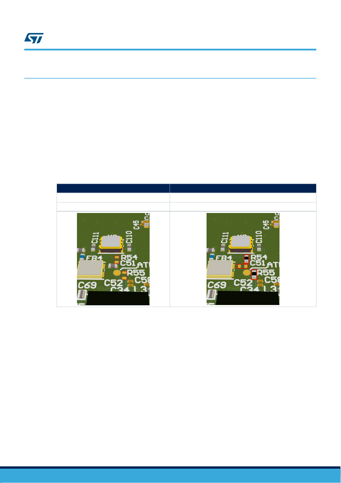
Table 1. TCXO/Crystal Configuration
Default configuration Alternate configuration (user configuration)
TCXO connected to ST25RU3993 Crystal connected to ST25RU3993
R54 and R55 not populated C51 removed and populate R54 and R55
The output of the internal PLL- charge pump is connected to LF_CEXT (pin 45) at which the external part of the
loop filter is placed in close proximity. An additional low pass filter stage is integrated in ST25RU3993 and is part
of the loop filter circuit. The loop filter output is the control voltage of the internal VCO. The carrier frequency is
modulated by the ASK or PR-ASK shaped modulation signal.
ST25RU3993 has two differential output port pairs:
• The 0-dBm (linear) output
• The internal power amplifier output
Depending on which differential output port pair is activated the modulated carrier frequency will be amplified
accordingly.
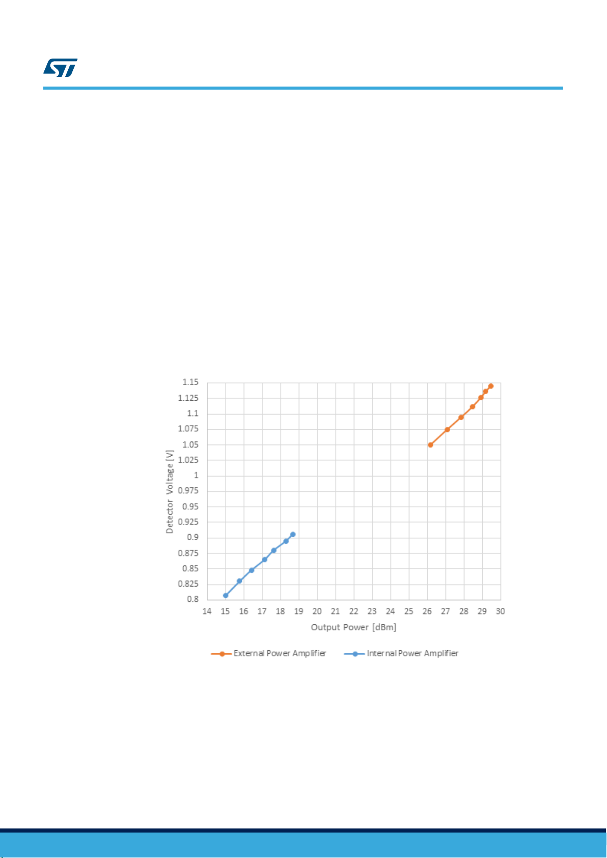
The 0-dBm output is used for the long-range configuration of the ST25RU3993-EVAL reader. The 0-dBm output
with its differential output pin pairs RFONX (23) and RFOPX (24) is connected to a 2:1 Balun at which point the
transmit signal is transformed from a 100 differential to a 50 Ω single-ended signal. The output stage of the 0-dBm
output is supplied by the VDD_B voltage that is generated and regulated by ST25RU3993. L3 and L4 act as a RF
choke, C57 and C58 as bypass capacitors and C65 and C54 as DC blocking capacitors. The signal then
proceeds to the external power amplifier to generate a high power output signal with approximately 31 dBm in
default configuration of ST25RU3993-EVAL board.
The internal power amplifier is used for the short-range configuration of the ST25RU3993-EVAL reader. The
output pins for the internal power amplifier are PAOUT_N (16, 17) and PAOUT_P (20, 21). A matching network
UM2353
Hardware description
UM2353 - Rev 2 page 7/48

and an 1:1 Balun transform the output of the internal power amplifier to a 50 Ω single-ended signal. The internal
power amplifier is supplied by the on-chip generated and regulated voltage VDD_PA.
L1, L2 act as RF chokes, C12 and C14 are bypass capacitors. After the Balun the output power of the internal
power amplifier can be measured as being approximately 21 dBm when switched to the short range configuration.
The output of the external power amplifier and the output of the internal power amplifier are connected to an RF-
switch, which can be controlled via the GUI of the ST25RU3993-EVAL reader. Only one power amplifier option
can be active at a time.
Note that in a typical reader design only one power amplifier option will be used depending on the application and
read range requirements. So for a commercial reader design the RF-switch will be removed and so it’s introduced
insertion loss of ~0.5 dB.
The RF-switch requires DC blocking capacitors on all its RF terminal. The output of the RF-switch is connected to
a low pass filter, which should attenuate the second and third harmonic of the carrier frequency.
The filtered transmit signal is then connected to a 20 dB directional coupler, which takes a portion of the transmit
power (<10 mW). This sample power is further attenuated by a pi-pad attenuator to limit the input power of the
logarithmic power detector. The power detector generates a DC voltage, which corresponds to the transmit power.
The characteristic of output DC voltage of the power detector versus the generated RF power is shown in the
chart below.
Figure 6. Power detector voltage characteristic
The DC output of the power detector is connected to an ADC (PA1) of the microcontroller.
After the 20 dB directional coupler the main directional coupler is placed, which has a coupling factor of 10 dB.
The purpose of this device is to isolate the transmit signal from the receiving inputs of ST25RU3993 and has
thereby a major influence on the sensitivity of the reader.
The output port of the main directional coupler is connected to a second RF-switch that allows to direct the
transmit power to either antenna port 1 or antenna port 2. The RF-switch again requires DC blocking capacitors
on all its RF terminal. The antenna ports both are of SMB (female) type.
In order to maintain the sensitivity of the reader the self-jamming signal reaching the receive inputs of
ST25RU3993 need to be minimized. The self-jamming signal comprises of reflections from the antenna (S11) and
UM2353
RF circuit
UM2353 - Rev 2 page 8/48

the leakage across the main directional coupler. To minimize the self-jamming signal a carrier cancellation circuit
is connected to the coupled port of the main directional coupler.
The carrier cancellation circuit is able to change its impedance and thereby is able to reflect a certain amount of
the coupled power back into the directional coupler again. This reflected signal will combine at the isolated port of
the main directional coupler with the self-jamming signal. The isolated port of the main directional coupler is
connected to the receive pins of ST25RU3993. In theory, if the signal reflected by the carrier cancellation circuit
has the same amplitude and the opposite phase then the self-jamming signal would cancel-out and vanishes.
To find the impedance setting of the carrier cancellation circuit that would result to a self-jamming signal
cancellation the power of the self-jamming signal needs to be measured. Such a measurement capability is
provided by ST25RU3993 and is referred to as reflected power measurement. An optimal impedance setting of
the carrier cancellation circuit would result to low reflected power measurement result. The main components of
the carrier cancellation circuit are three digital tunable capacitors, which are controlled by the STM32L476RG
microcontroller via the SPI interface. The fixed lumped components of the carrier cancellation circuit help to
center its impedance to 50 Ω and define the impedance step created by one LSB change of a digital tunable
capacitor.
The isolated port of the main directional coupler is connected to a 2:1 Balun to transform the incoming tag
response signal to a 100 Ω differential signal that is fed into ST25RU3993 at the pins MIX_INP (4) and MIX_INN
(6).
5.2 Microcontroller and connections
Table 2. MCU interfaces and buttons
Button Description
A MCU reset button
B USB receptacle: micro, B-type
C JTAG interface: for BT module programming
D BT module reset button (not installed)
E BT module boot mode jumper (not installed)
F UART interface connections
G MCU Boot mode button
HSTM32L476RGT6 (Arm® 32-bit Cortex®-M4)
J SWD debug interface connections
K, L and M SPI debug interface connections
N UART_LOG connection for debugging purposes
P Enable power amplifier LDO
RST25RU3993 RAIN® (UHF) RFID reader device
UM2353
Microcontroller and connections
UM2353 - Rev 2 page 9/48

Figure 7. Main digital interfaces
The ST25RU3993-EVAL is controlled by STM32L476RGT6 (U1), which is an ultra-low-power microcontroller with
FPU Arm® 32-bit Cortex®-M4 MCU 80 MHz with 1 Mbyte Flash, LCD, USB OTG, DFSDM.
UM2353
Microcontroller and connections
UM2353 - Rev 2 page 10/48

STM32L476RGT6 is supplied by 3.3 volts, which is regulated by an LDO (U9). The clock source for
STM32L476RGT6 is an external crystal (X1) generating 32.768 kHz and is connected to OSC32_in (3) and
OSC32_out (4).
The STM32L476RGT6 microcontroller communicates with the host PC via UART for which an USB/UART bridge
is used.
The STM32L476RGT6 communicates with ST25RU3993 (U5) by the SPI interface, the ENABLE and IRQ line.
The SPI interface operates in mode 1 with a 4 MHz serial clock. The SPI interface is also used to control the
digital tunable capacitors for the carrier cancellation circuit.
The STM32L476RGT6 also controls the RF switches for changing the power amplifier and changing the active
antenna port. The analog output of the RF power detector is connected to one of the ADC inputs (PA1) of
STM32L476RGT6 to convert the RF power into a digital format. The LDO (U11) for the external power amplifier is
controlled by the STM32L476RGT6, which completely shuts down the external power amplifier when RF power
needs to be OFF. E.g. Carrier Sense (LBT).
One pin (UART LOG) is reserved to act as a generic debug pin that can be programmed as a trigger pin for an
external measurement equipment. The optional (not installed) BT module connects with the STM32L476RG with
its second UART interface.
Table 3. MCU - SPI interface and ST25RU3993 connections
Component: U1 Component: U5 Component: U6 Component: U7 Component: U8
MCU pin
name
MCU pin
number
ST25RU3993 pin
name
ST25RU3993 pin
number
DTC1 pin
name
DTC1 pin
number
DTC2 pin
name
DTC2 pin
number
DTC3 pin
name
DTC3 pin
number
PA4 20 NCS 33 - - - - - -
PA5 21 CLK 37 CLK 5 CLK 5 CLK 5
PA6 22 MISO 34 - - - - - -
PA7 23 MOSI 35 SDAT 7 SDAT 7 SDAT 7
PC7 38 - - - - - - SEN 6
PC8 39 - - - - SEN 6 - -
PC9 40 - - SEN 6 - - - -
PA9 42 IRQ 32 - - - - - -
PA10 43 EN 31 - - - - - -
UM2353
Microcontroller and connections
UM2353 - Rev 2 page 11/48

Table 4. SPI interface pinout at J10, J12 and J13
Component: U5 Component: U6 Component: U7 Component: U8
J10 J12 J13
ST25RU3993 pin
name
ST25RU3993 pin
number
DTC1 pin
name
DTC1 pin
number
DTC2 pin
name
DTC2 pin
number
DTC3 pin
name
DTC3 pin
number
SCLK 37 CLK 5 CLK 5 CLK 5 1 - -
MISO 34 - - - - - - 3 - -
MOSI 35 SDAT 7 SDAT 7 SDAT 7 2 - -
- - - - - - ETC3
SEN 6 - - 3
- - - - ETC2
SEN 6 - - - - 2
- - ETC2
SEN 6 - - - - - - 1
OAD2 - - - - - - 1 -
OAD - - - - - - - - 2 -
EN 31 - - - - - - - 3 -
IRQ 32 - - - - - - - 4 -
NCS 33 - - - - - - - 5 -
ADC - - - - - - - - 6 -
Table 5. UART connections and pinout
Component: U1 Component: U13 J7
MCU pin name MCUpin number FTDI pin name FTDI pin number Connector pin number
NRST 7 RTS 19 1
BOOT0 60 DTR 18 2
PA3 17 TXD 17 3
PA2 16 RXD 1 4
Table 6. MCU - connections to buttons
Component: U1 Component: B1 Component: B2
MCU pin name MCU pin number Reset button pin name Reset button pin
number Boot button pin name Boot button pin number
NRST 7 1 1 - -
NRST 7 4 4 - -
BOOT0 60 - - 2 2
BOOT0 60 - - 5 5
UM2353
Microcontroller and connections
UM2353 - Rev 2 page 12/48

Table 7. MCU - Connections to LEDs
Component: U1 D1 D2 D3 D4 D5 D6 D7 D8 D11 D12 D13 D16 D17
MCU
pin
name
MCU pin
number
MCU_LED
intPA_LED
RF_LED
extPA_LED
TUNING_LED
TAG_LED
PLL_LED
OSC_LED
TUNED_LED
NO_RESP_LED
CRC_ERR_LED
ANT1_LED
ANT2_LED
PA0 14 1 (C) - - - - - - - - - - - -
PD2 54 - 1(C) - - - - - - - - - - -
PC10 51 - - 1(C) - - - - - - - - - -
PB4 56 - - - 1(C) - - - - - - - - -
PC12 53 - - - - 1(C) - - - - - - - -
PC6 37 - - - - - 1(C) - - - - - - -
PB12 33 - - - - - - 1(C) - - - - - -
PB13 34 - - - - - - - 1(C) - - - - -
PC11 52 - - - - - - - - 1(C) - - - -
PB14 35 - - - - - - - - - 1(C) - - -
PB15 36 - - - - - - - - - - 1(C) - -
PB2 28 - - - - - - - - - - - 1(C) -
PB1 27 - - - - - - - - - - - - 1(C)
Table 8. MCU - connections to RF switches
Component: U1 Component: S1 Component: S2
MCU pin name MCU pin number PA switch
pin name
PA switch
pin number Antenna switch pin name Antenna switch pin number
PB0 26 V1 1 - -
PC5 25 V2 3 - -
PB10 29 - - V1 1
PB11 30 - - V2 3
Table 9. MCU - connections to BT module
Component: U1 Component: S1
MCU pin name MCU pin number BT module
pin name
BT module
pin number
PA11 44 RTS 12
PA12 45 CTS 11
PB6 58 RXD 13
PB7 59 TXD 14
PC13 2 RESETn 10
PB9 62 BOOT0 9
UM2353
Microcontroller and connections
UM2353 - Rev 2 page 13/48

Table 10. MCU - connections to JTAG interface and pinout
Component: U12 Component: J14
MCU pin name MCU pin number JTAG
pin name
JTAG
pin number
JNTRST 20 RST 1
JTDO 22 DO 2
JTCK 24 CK 3
JTMS 21 MS 4
JTDI 23 DI 5
NRST 19 nR 6
- - 3V3 7
- - GND 8
Table 11. MCU - connections to JLINK (SWD) interface and Pinout of connector
Component: U1 Component: P3
MCU pin name MCU pin number JLINK
pin name
JLINK
pin number
- - 3V3 1
PA13 46 SWDIO 2
- - GND 3
PA14 49 SWCLK 4
- - GND 5
PB3 55 SWO 6
- - NC 7
PA15 50 TDI 8
- - NC 9
NRST 7 MCU_RESET_N 10
5.3 Firmware programming
There are two options how to program the firmware of the STM32L476RG microcontroller:
1. The simplest way to program a new firmware version to the MCU is by connecting the ST25RU3993-EVAL
board to the host PC with the micro USB cable and use the “Firmware Update” function of the GUI. For more
information about this option refer to the user manual of the GUI.
2. Alternatively the firmware can be programmed to the MCU using the ST-LINK connecting to the JLINK
(SWD) interface with an J-Link Needle Adapter (e.g.: Digikey: 899-1047-ND). For more information about
this option refer to the user manual of the ST-LINK/V2.
UM2353
Firmware programming
UM2353 - Rev 2 page 14/48

5.4 Boot mode
To enter the boot mode of the STM32L476RG microcontroller press and hold the Boot button(1) then press the
RESET button(2). At this point the boot mode is active and both buttons can be released.
Figure 8. Entering the boot mode
5.5 Power supply
The ST25RU3993-EVAL is supplied by the USB 3.0 port of the host PC. An USB 3.0 port is required if the long
range configuration using the external PA is set.
If an USB 3.0 port is not available an USB 2.0 Y-cable or an external power supply can be used to enable the long
range capabilities of reader.
If neither is available only the short range reader configuration with lower RF power is available. If the
ST25RU3993-EVAL board is configured as short range reader using the internal PA an USB 2.0 port would
suffice.
In order to observe and measure the current consumption of the entire reader a 2-pin header is available. In
normal operation this 2-pin header is shorted by an jumper. To measure the current consumption remove the
jumper and connect an ampere meter in series instead.
To connect an external 5 V supply see Figure 9.
UM2353
Boot mode
UM2353 - Rev 2 page 15/48

Figure 9. Connecting an external supply voltage
The 5 V (VBUS) of the USB port is connected to three low-dropout regulators, which supply:
• Digital components
• RF components
• External power amplifier
For the digital components a 3.3 V supply is provided. RF components are supplied by 3.6 V and the external
power amplifier is supplied by 4.1 V.
Table 12. Typical voltage levels
Voltage domain Typical voltage level
3V3 3.33
VSUP 3.67
VPA 4.1
Table 13. Components connected to 5 V
5 V
Schematic page Component Pin name Pin number
Supply U9, U10, U11 VI 6
Supply U9, U10 EN 1
USB_Interface U13 VCC 12
UM2353
Power supply
UM2353 - Rev 2 page 16/48

Table 14. Digital components connected to 3V3 (3.3 V)
3V3 (3.3 V)
Schematic page Component Pin name Pin number
External_Interfaces P3 1 1
External_Interfaces J14 7 7
External_Interfaces U1 VBAT 1
Controller U1 VDD 19, 32, 48, 64
Controller U1 VDDA/VREF+ (1) 13
Controller U1 NRST(2) 7
Controller U1 BOOT0(3) 60
Controller D1-D8, D11-D13, D16, D17 - 1
Power_Amplifier U3 VCC 8
UHF_RFID U4 VCC(4) 4
UHF_RFID U5 VDD_IO 38
Carrier_Cancellation U6, U7, U8 VDD 4
Bluetooth U12 VIN(5) 8
Bluetooth U12 BOOT0(6) 9
Bluetooth B14 - 1
USB_Interface U12 VCCIO 20
1. Via ferrite bead FB3.
2. Via pull up resistor R61.
3. Via push button B2.
4. Via ferrite bead FB4.
5. Via ferrite bead FB2.
6. Via J19.
Table 15. Components connected to VSUP (3.6 V)
VSUP (3.6 V)
Schematic page Component Pin name Pin number
UHF_RFID U5 VEXT (1) 11
UHF_RFID U5 VEXT_PA(2) 14
1. Via ferrite bead FB5.
2. Via ferrite bead FB1.
Table 16. Components connected to VPA (4.1 V)
VPA (4.1 V)
Schematic page Component Pin name Pin number
Power_Amplifier U2 VPD1 12
Power_Amplifier U2 VPD2 11
Power_Amplifier U2 VCC 2
Power_Amplifier U2 VBIAS (1) 1
1. Via R21.
UM2353
Power supply
UM2353 - Rev 2 page 17/48

5.6 Test Points
The ST25RU3993-EVAL board provides numerous test points to test and to evaluate the ST25RU3993 reader
device, and important circuit nodes in the reader design.
Figure 10. Test points
UM2353
Test points
UM2353 - Rev 2 page 18/48

5.6.1 Analog test points
Table 17. Analog test point connections
Component: U5 Component: U2 Component: U3
Analog
test point
ST25RU3993
pin name
ST25RU3993
pin number
PA
pin name
PA
pin number
Power det.
pin name
Power det.
pin number
OSCO 30 - - - - ATP1
VCO (LF_CEXT) 45 - - - - ATP2
- - VBIAS 1 - - ATP3
- - - - OUT 7 ATP4
5.6.2 Supply voltage test points
Table 18. Supply voltage test points
5 V external supply 3V3 digital supply VSUP RF supply VPA power amplifier supply
P2 J5 J20 J21
Pin number Pin name Pin number Pin name Pin number Pin name Pin number Pin name
1 VBUS 1 GND 1 GND 1 GND
2 VBUS 2 3V3 2 VSUP 2 VPA
- - 3 3V3 3 VSUP 3 VPA
Supply voltage measurement
At the output of each of the three LDOs two test points are placed in order to conveniently measure the regulated
voltage of each voltage domain. A GND pad is placed directly next to the voltage test point to allow accurate
voltage measurements.
Example:
Figure 11. Connection a voltmeter to the supply voltage test points
Current Consumption Measurement
The current consumption flowing into each of the three voltage domains can be measured separately. To enable
this kind of measurement a 0 Ω resistor needs to be removed. Make sure to establish a connection again once
the measurement is done reverting to normal operation.
Example:
UM2353
Test points
UM2353 - Rev 2 page 19/48

Figure 12. Connection an ampere meter to the supply voltage test points
5.6.3 Digital test points
In addition to the four test points shown above a test point for each LED, connected to the STM32L476RG
controller is placed.
PLL OK:
Indicates that the PLL of ST25RU3993 is locked and the carrier frequency is stable.
OSC OK:
Low active. Indicates that the reference frequency for the PLL is stable.
No Tag Response:
Is pulled low if the sent reader command is not replied by a tag.
Tag CRC Error:
Is pulled low if a CRC error is detected within a tag response.
Tag found:
Is pulled low every time a tag has been inventoried.
EXT_PA:
Is pulled low if the reader is in its long range configuration.
INT_PA:
Is pulled low if the reader is in its short range configuration.
TUNING:
Is pulled low if the reader currently is re-tuning the carrier cancellation circuit.
Tuned:
Low active. Indicates that the self-jamming signal is sufficiently suppressed.
RF ON:
Low active. Indicates that the RF carrier is ON.
ANT1:
Low active. Indicates that antenna port 1 is active.
UM2353
Test points
UM2353 - Rev 2 page 20/48
Table of contents
Other ST Motherboard manuals

ST
ST STM32MP157D-EV1 User manual

ST
ST SPC572LADPT80S User manual

ST
ST FP-SNS-6LPNODE1 User manual

ST
ST STM8L101-EVAL User manual

ST
ST EVALST-3PHISOSD User manual

ST
ST SPC574KADPT144S User manual

ST
ST SPC58XXMB User manual

ST
ST STEVAL-LLL011V1 User manual

ST
ST STLINK-V3SEGT User manual

ST
ST NUCLEO-F411RE Manual

ST
ST SGS-Thomson ST624x-KIT Series User manual

ST
ST STM3220G-EVAL User manual

ST
ST STM32L4 Series User manual

ST
ST FDA803S User manual

ST
ST STSW-S2LP-KNX-DK User manual

ST
ST STM32L1 Series Installation and operating instructions

ST
ST EVAL-L99DZ200 User manual

ST
ST STM32H753I-EVAL User manual

ST
ST STSW-STUSB002 User manual

ST
ST STUSB03E User manual