SONIX SNC7320 Series User manual

SNC7320 Series
Evaluation Board Manual
www.sonix.com.tw
1
SEVB-18ZA
About This Document
This purpose of this document is to provide steps on how to setup the evaluation (EV) board.
Revision History
Date
Revision
Description
08-Jul-2018
PCB V1.1
Initial release
21-Nov-2018
Bottom PCB V2
Update bottom PCB V2
22-Nov-2018
Document Preview A
Initial release
Convention
WARNING
Indicates a hazard with a medium or low level of risk that, if not avoided, could result
in minor or moderate injury.
TIP
Indicates a tip that may help you solve a problem or save time.
NOTE
Provides additional information to emphasize or supplement important points of the
main text.

SNC7320 Series
Evaluation Board Manual
www.sonix.com.tw
2
SEVB-18ZA
Table of Contents
Convention...................................................................................................................................................1
Table of Contents.........................................................................................................................................2
List of Figures ..............................................................................................................................................3
Overview...............................................................................................................................................41Interface Connectors ............................................................................................................................722.1 Introduction.................................................................................................................................7
2.2 AC Adapter Connector and BAT Connector................................................................................7
2.2.1 Circuit Diagrams ...........................................................................................................9
2.3 J-Link Connector.......................................................................................................................10
2.3.1 Circuit Diagram...........................................................................................................11
2.4 CIS/Y Sensor Connector...........................................................................................................11
2.4.1 Circuit Diagram...........................................................................................................12
2.5 NAND Flash/SD Card Connector..............................................................................................13
2.5.1 Circuit Diagram...........................................................................................................14
2.6 SDIO/SD Slot............................................................................................................................14
2.6.1 Circuit Diagram...........................................................................................................15
2.7 EHCI Host Connector (USB_H)................................................................................................15
2.7.1 Circuit Diagram...........................................................................................................16
2.8 USB Device Connector (USB_D)..............................................................................................16
2.8.1 Circuit Diagram...........................................................................................................17
2.9 Reset Key/ISO WKP Key..........................................................................................................17
2.9.1 Circuit Diagram...........................................................................................................18
2.10 UART/Debug Connector...........................................................................................................18
2.10.1 Circuit Diagram...........................................................................................................19
2.11 SPI Flash Connector................................................................................................................. 20
2.11.1 Circuit Diagram...........................................................................................................20
2.12 TFT/8080 Connector................................................................................................................. 21
2.12.1 Circuit Diagram...........................................................................................................21
2.13 I2S Connector............................................................................................................................22
2.13.1 Circuit Diagram...........................................................................................................22
2.14 SAR ADC/PWM Connector.......................................................................................................23
2.14.1 Circuit Diagram...........................................................................................................23
Connector Pin Assignments................................................................................................................2433.1 J-Link Connector (J2)................................................................................................................24
3.2 CIS Connector (CN5)................................................................................................................ 24
3.3 SD Card0/I2C Connector (J5)....................................................................................................25
3.4 SPI Flash Connector (J8)..........................................................................................................25
3.5 TFT/8080 Connector (J4)..........................................................................................................26
3.6 I2S Connector (J9).....................................................................................................................27
3.7 SAR ADC/PWM Connector (J13)..............................................................................................27
3.8 GPIO Pin Assignments .............................................................................................................27
Layout Overview.................................................................................................................................29
4

SNC7320 Series
Evaluation Board Manual
www.sonix.com.tw
3
SEVB-18ZA
List of Figures
Figure 1–1Top View of SNC7320_EV_Board_Top-Vx.x......................................................................4
Figure 1–2Top View of SNC7320_EV_Board_Bottom-Vx.x.................................................................5
Figure 1–3Top View of SNC7320_Debug_Board_Vx.x .......................................................................6
Figure 2–1AC Adapter Connector of Bottom Board.............................................................................8
Figure 2–2Battery Connector of Top Board .........................................................................................8
Figure 2–3Circuit Diagram of AC Adapter Connector..........................................................................9
Figure 2–4Circuit Diagram of Battery Connector .................................................................................9
Figure 2–5J-Link Connector of Top Board......................................................................................... 10
Figure 2–6J-Link Connector of Bottom Board....................................................................................10
Figure 2–7Circuit Diagram of JTAG...................................................................................................11
Figure 2–8CIS Connector ..................................................................................................................11
Figure 2–9Y Sensor Connector..........................................................................................................11
Figure 2–10 Circuit Diagram of the CIS Connector...............................................................................12
Figure 2–11 Circuit Diagram of the Y Sensor Connector......................................................................12
Figure 2–12 NAND Flash Connector ....................................................................................................13
Figure 2–13 SD Card Connector...........................................................................................................13
Figure 2–14 Circuit Diagram of the NAND Flash/SD Card Connector..................................................14
Figure 2–15 SDIO/SD Slot and SD CS/WP Pin....................................................................................14
Figure 2–16 Circuit Diagram of the SDIO/SD Connector......................................................................15
Figure 2–17 EHCI Host Connectors......................................................................................................15
Figure 2–18 Circuit Diagram of the USB Host and WiFi Module........................................................... 16
Figure 2–19 USB Device Connector.....................................................................................................16
Figure 2–20 Circuit Diagram of a USB Device...................................................................................... 17
Figure 2–21 RESET and ISO WKP.......................................................................................................17
Figure 2–22 Circuit Diagram of RESET and ISO WKP.........................................................................18
Figure 2–23 UART Connector of Top Board.........................................................................................18
Figure 2–24 UART Connector of Bottom Board....................................................................................19
Figure 2–25 Circuit Diagram of UART/Debug.......................................................................................19
Figure 2–26 SPI Flash Connector.........................................................................................................20
Figure 2–27 Circuit Diagram of SPI Flash Connector...........................................................................20
Figure 2–28 TFT/8080 Connector.........................................................................................................21
Figure 2–29 Circuit Diagram of the 8/16/18-bit RGB and 8080 TFT.....................................................21
Figure 2–30 I2S Connector....................................................................................................................22
Figure 2–31 Circuit Diagram of the I2S Connector................................................................................22
Figure 2–32 SAR ADC/PWM Connector...............................................................................................23
Figure 2–33 Circuit Diagram of the SAR ADC/PWM Connector...........................................................23
Figure 4–1Top View of the 7320_EV_Board_Top-Vx.x .....................................................................29
Figure 4–2Bottom View of the 7320_EV_Board_Top-Vx.x................................................................29
Figure 4–3Top View of the 7320_EV_Board_ Bottom-Vx.x ...............................................................30
Figure 4–4Top View of the 7320_EV_Board_ Bottom-Vx.x ...............................................................31

SNC7320 Series
Evaluation Board Manual
www.sonix.com.tw
4
SEVB-18ZA
Overview1
The evaluation board of the SNC7320 Series consists of:
•SNC7320_EV_Board_Top-Vx.x
1
: Top board
•SNC7320_EV_Board_Bottom-Vx.x: Bottom board
•SNC7320_Debug_Board_Vx.x: Debug board
Top view of each board and the names of the components are provided below.
Figure 1–1 Top View of SNC7320_EV_Board_Top-Vx.x
Names of the components corresponding to the numbers on the figure above are:
1. Battery Connector
2. Debug IF Connector
3. CMOS Image Sensor (CIS)
4. Y Sensor
5. Hardware Reset Key
6. SD Card CD/WP Pin
7. ISO Wakeup Key
8. SDIO/SD Connector
9. SPI F Flash Connector
10. USB Host (EHCI) Connector
11. Micro-USB Device Connector
1
x = a variable number; may change as the version gets updated.

SNC7320 Series
Evaluation Board Manual
www.sonix.com.tw
5
SEVB-18ZA
Figure 1–2 Top View of SNC7320_EV_Board_Bottom-Vx.x
Names of the components corresponding to the numbers on the figure above are:
1. Power-7.5V AC adapter
2. LED x4
3. Key x4
4. TFT/8080 Connector
5. SD Card/NAND Flash/GPIO3 Connector
6. Audio Connectors: I2S 0–3, I2C 1–2
7. SAR0/PWM Interface
8. I2C Interface Connector
9. I2S4 Interface
10. SNC7320_EV_Board_Top-Vx.x Connector
11. RF Board Interface
12. SPI0 Interface Connector
13. Debug IF Connector
14. SPI1 Interface Connector
15. RF Board Interface
16. SD Card/NAND Flash/TFT Connector
8
8
1
1
2
2
10
10
9
9
3
3
4
4
5
5
6
6
11
11
13
13
14
14
15
15
12
12
16
16
7
78
8
8
8

SNC7320 Series
Evaluation Board Manual
www.sonix.com.tw
6
SEVB-18ZA
Figure 1–3 Top View of SNC7320_Debug_Board_Vx.x
Names of the components corresponding to the numbers on the figure above are:
1. UART Interface Connector
2. JTAG Emulator Connector
3. Debug IF to connect the Debug IF pin of SNC7320_EV_Board_Bottom-Vx.x and
SNC7320_EV_Board_Top-Vx.x

SNC7320 Series
Evaluation Board Manual
www.sonix.com.tw
7
SEVB-18ZA
Interface Connectors2
2.1 Introduction
2.2 AC Adapter Connector and BAT Connector
2.3 J-Link Connector
2.4 CIS/Y Sensor Connector
2.5 NAND Flash/SD Card
2.6 SDIO/SD Slot
2.7 EHCI Host Connector (USB_H)
2.8 USB Device Connector (USB_D)
2.9 Reset Key/ISO WKP Key
2.10 UART/Debug
2.11 SPI Flash Connector
2.12 TFT/8080 Connector
2.13 I2S Connector
2.14 SAR ADC/PWM Connector
2.1 Introduction
The SNC7320_EV_Board_Top-Vx.x and the SNC7320_EV_Board_Bottom-Vx.x are a full function
development system. They provide various interfaces such as CIS, SD card, NOR/NAND flash,
SRAM, 8080 LCM, TFT LCD, Audio (I2S), USB (device or host), SAR ADC, SPI, I2C, UART, and …etc.
for development of wide range of applications. The subsections below explain how to use each
connector and provide circuit diagrams thereof.
2.2 AC Adapter Connector and BAT Connector
There are two power processes on SNC7320 EVB. Their relative of power domain on
SNC7320_EV_Board_Bottom-Vx.x and SNC7320_EV_Board_Top-Vx.x can depart into two cases
below.
Case 1: Use the AC adapter connector (J2) of the bottom board to supply power to the EVB. The
bottom board converts the voltage from 7.5V to 5V with a 7805 regulator, and supplies 5V power to the
top board. The top board converts the 5V power to 3.3Vand provides 3.3V power to the bottom board
and the peripherals connected to it.

SNC7320 Series
Evaluation Board Manual
www.sonix.com.tw
8
SEVB-18ZA
Figure 2–1 AC Adapter Connector of Bottom Board
Case 2: Use a battery to supply power to the EVB via connector J2 of the bottom board.
The supplies 3.3V power to the peripherals connected to the bottom board after the top board
converting power from 5V to 3.3V.
Figure 2–2 Battery Connector of Top Board
J2
J2
JP1
JP1
JP1
JP1
J2
J2
-
+
-
+

SNC7320 Series
Evaluation Board Manual
www.sonix.com.tw
9
SEVB-18ZA
2.2.1 Circuit Diagrams
Figure 2–3 Circuit Diagram of AC Adapter Connector
Figure 2–4 Circuit Diagram of Battery Connector
NOTE
When using the SNC7320 EV Board, remember to short JP1for the power
supply of the IC and peripherals.

SNC7320 Series
Evaluation Board Manual
www.sonix.com.tw
10
SEVB-18ZA
2.3 J-Link Connector
Case 1: When the bottom board is not attached, connect the debug board to the top board with
connector J9. The connector J2 is the connector for J-Link.
Figure 2–5 J-Link Connector of Top Board
Case 2: When the top and bottom boards are both attached, connect the debug board to the bottom
board with connector J12. The connector J2 is the connector for the J-Link.
Figure 2–6 J-Link Connector of Bottom Board
J12
J12
J2
J2

SNC7320 Series
Evaluation Board Manual
www.sonix.com.tw
11
SEVB-18ZA
2.3.1 Circuit Diagram
Figure 2–7 Circuit Diagram of JTAG
2.4 CIS/Y Sensor Connector
Connector CN5 of the top board connects the CIS interface. Since the CIS uses I2C to initialize the
CIS sensor, the connector CN5 includes an I2C interface.
Figure 2–8 CIS Connector
The connector CN6 of the top board connects the Y sensor interface.
Figure 2–9 Y Sensor Connector

SNC7320 Series
Evaluation Board Manual
www.sonix.com.tw
12
SEVB-18ZA
2.4.1 Circuit Diagram
Figure 2–10 Circuit Diagram of the CIS Connector
Figure 2–11 Circuit Diagram of the Y Sensor Connector

SNC7320 Series
Evaluation Board Manual
www.sonix.com.tw
13
SEVB-18ZA
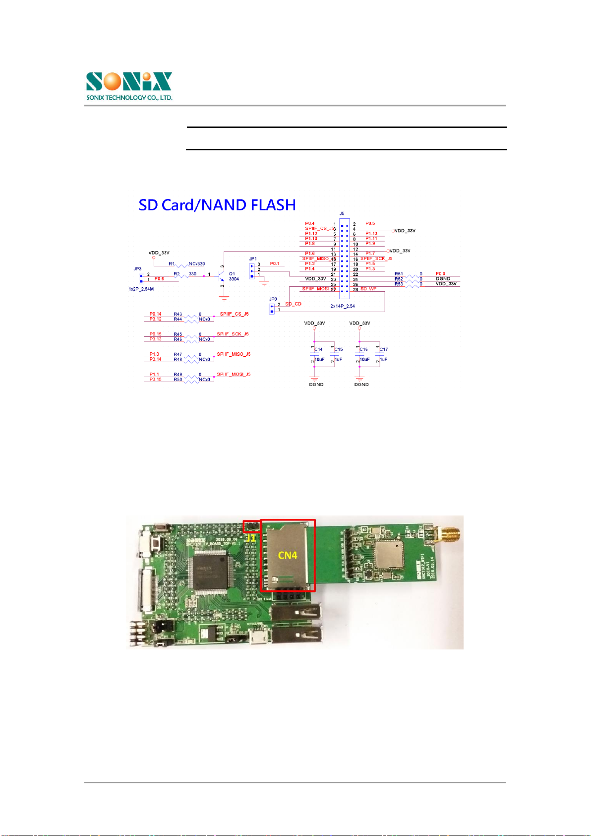
2.5 NAND Flash/SD Card Connector
Connector J5 is for the NAND flash/SD card interface.
Figure 2–12 NAND Flash Connector
Figure 2–13 SD Card Connector
J5
J5
J5
J5
SNC7320 Series
Evaluation Board Manual
www.sonix.com.tw
14
SEVB-18ZA
NOTE
When using the SD card, remember to shorten J6 to SDC mode for proper
functioning.
2.5.1 Circuit Diagram
Figure 2–14 Circuit Diagram of the NAND Flash/SD Card Connector
2.6 SDIO/SD Slot
The slot shown in the figure below is the slot of the SDIO/SD (CN4) on the top board. J1 is the SD
CD/WP pin.
Figure 2–15 SDIO/SD Slot and SD CS/WP Pin

SNC7320 Series
Evaluation Board Manual
www.sonix.com.tw
15
SEVB-18ZA
2.6.1 Circuit Diagram
Figure 2–16 Circuit Diagram of the SDIO/SD Connector
2.7 EHCI Host Connector (USB_H)
The connectors Host 1 (CN2) and Host 2 (CN3) are for the USB EHCI, also known as USB_H.
Figure 2–17 EHCI Host Connectors
NOTE
When using the USB host module, remember to short JP3 for proper
functioning. Connect JP4 to 5V.
CN3
CN3
CN2
CN2
JP3
JP3JP4
JP4

SNC7320 Series
Evaluation Board Manual
www.sonix.com.tw
16
SEVB-18ZA
2.7.1 Circuit Diagram
Figure 2–18 Circuit Diagram of the USB Host and WiFi Module
2.8 USB Device Connector (USB_D)
The connector (CN1) is the plug in for a USB device, also known as USB_D.
Figure 2–19 USB Device Connector
CN1
CN1

SNC7320 Series
Evaluation Board Manual
www.sonix.com.tw
17
SEVB-18ZA
2.8.1 Circuit Diagram
Figure 2–20 Circuit Diagram of a USB Device
2.9 Reset Key/ISO WKP Key
The reset key of the top board is an external hardware reset of the chip. The ISO WKP key is the
external hardware wake up of the chip.
Figure 2–21 RESET and ISO WKP

SNC7320 Series
Evaluation Board Manual
www.sonix.com.tw
18
SEVB-18ZA
2.9.1 Circuit Diagram
Figure 2–22 Circuit Diagram of RESET and ISO WKP
2.10 UART/Debug Connector
Connector J9 of the top board and connector J12 of the bottom board connects the debug board. CN1
is for the UART.
Figure 2–23 UART Connector of Top Board

SNC7320 Series
Evaluation Board Manual
www.sonix.com.tw
19
SEVB-18ZA
Figure 2–24 UART Connector of Bottom Board
2.10.1 Circuit Diagram
Figure 2–25 Circuit Diagram of UART/Debug
J12
J12
CN1
CN1

SNC7320 Series
Evaluation Board Manual
www.sonix.com.tw
20
SEVB-18ZA
2.11 SPI Flash Connector
Connector J8 of the top board is the SPI flash connector as shown in the figure below.
Figure 2–26 SPI Flash Connector
2.11.1 Circuit Diagram
Figure 2–27 Circuit Diagram of SPI Flash Connector
Table of contents
Other SONIX Motherboard manuals


