Sony XDP-4000X Operating Instructions (primary... User manual

– 1 –
SERVICE MANUAL
SPECIFICATIONS
Power requirements 12 V DC car battery (negative
ground, 10.5 V – 16 V)
Current drain 1 A
Frequency response 5 Hz – 20 kHz
Signal-to-noise ratio 105 dB (Optical input)
Harmonic distortion 0.003 % (Optical input)
Separation 95 dB at 1 kHz
Input/output terminals BUS input (1)
BUS output (1)
Line input (RCA jack) (2)
Line output (RCA jack) (4)
Optical digital input (2)
Dimensions Approx. 249 ×45 ×183 mm
(9 7/8 ×1 13/16 ×7 1/4 in.) (w/h/d)
Mass Approx. 2 kg (4 lb. 7 oz.)
Design and specifications are subject to change without
notice.
XDP-4000X
US Model
Canadian Model
AEP Model
UK Model
E Model
DIGITAL EQUALIZER PREAMPLIFIER
MICROFILM
Notes on Chip Component Replacement
•Never reuse a disconnected chip component.
•Notice that the minus side of a tantalum capacitor may be dam-
aged by heat.

– 2 –
SECTION 1
SERVICE NOTE
TABLE OF CONTENTS
1. SERVICE NOTE................................................................. 2
2. GENERAL
Operation ................................................................................. 4
Connection............................................................................... 5
3. DISASSEMBLY
3-1. Case (Upper)....................................................................... 7
3-2. Main Board......................................................................... 7
4. DIAGRAMS
4-1. IC Pin Descriptions ............................................................ 8
4-2. Block Diagram – Input section –...................................... 15
4-3. Block Diagram – DSP section –....................................... 17
4-4. Block Diagram – Output section – ................................... 19
4-5. Printed Wiring Board – Main Section – ........................... 21
4-6. Schematic Diagram – Main Section (1/4) – ..................... 25
4-7. Schematic Diagram – Main Section (2/4) – ..................... 27
4-8. Schematic Diagram – Main Section (3/4) – ..................... 29
4-9. Schematic Diagram – Main Section (4/4) – ..................... 31
4-10. Schematic Diagram – DAC, Intelligence,
Indicator Section –............................................................ 33
4-11. Printed Wiring Board – DAC Section – ........................... 35
4-12. Printed Wiring Boards – Intelligence,
Indicator Section –............................................................ 37
5. EXPLODEDVIEW........................................................... 43
6. ELECTRICAL PARTS LIST......................................... 44
+
–
BATT,ACC
GND
master unit
regulated DC
power supply
(14.4V)
+
–
B+
GND
regulated DC
power supply
(14.4V)
BUS CONTROL IN
BUS CONTROL IN
(MASTER)
XDP-4000X
METHOD OF OPERATINGTHE XDP-4000X
This set cannot be operated alone.
To operated this, it should be connected with a master unit such as
CDX-C880 or XR-C9100 as shown below.

– 3 –
12345
6 7 8 9
METHOD OF DETERMINING ACCEPTANCE OR REJECTION OF
INTELLIGENCE BOARD (A-3317-137-A) OF XDP-4000X
• No parts in the intelligence board can be repaired.
If the intelligence board is defective, the whole board
should be replaced.
Pin numbers of 9-pin D-SUB connector (CN707)
(viewed from the top of the set)
Note that the voltage given in the following
descriptions is relative to the ground power pin.
Intelligence board check
Is voltage at pin !º of IC707 +5V?
Is voltage at pin 3of CN707
between –8 and –9V ?
Is the resistance between pin 1of CN703
and ground hundreds of 100 kilohms or more
Pull cable out of CN703 on main board.
Is voltage at pin 2of the CN703 +5V?
Intelligence board at fault
Intelligence board is normal
Main board at fault
Set ACC-OFF and pull cable out of
CN703 on main board
Main board at fault
Yes
Yes
Yes
Yes
Is voltage at pin 9of IC707 +5V?
Is voltage at pin 2of CN707 0V?
Is voltage at pin 9of IC707 0V?
Add –8 to –9V to pin 2of CN707
Yes
Yes
Yes
No
No
No
No
No
No
No
The fault of the main board may be caused by one of the
following:
1. Shorted CN703 (OPEN).
2. Shorted pins !™ and !¢ of IC702 (OPEN).
3. Damaged port of IC702.

– 4 –
This section is extracted
from instruction manual.
SECTION 2
GENERAL

– 5 –

– 6 –

– 7 –
SECTION 3
DISASSEMBLY
Note : Follow the disassembly procedure in the numerical order given.
3-1. CASE (UPPER)
3
ornamental plate assy
2
hexagon socket bolt (M4x6
)
1
hexagon socket bolt (M4x6)
4
CN706
5
CN703
6
PTT3x6
7
PTT3x6
8
PTT3x6
9
PTT3x6
0
case (upper)
3-2. MAIN BOARD
1
connectors
4
PTT3x6
3
PTT3x6
2
DAC board
5
PTP3x8
6
PTT2.6x8
7
PTP3x8
8
MAIN board
9
spacer

– 8 –
SECTION 4
DIAGRAMS
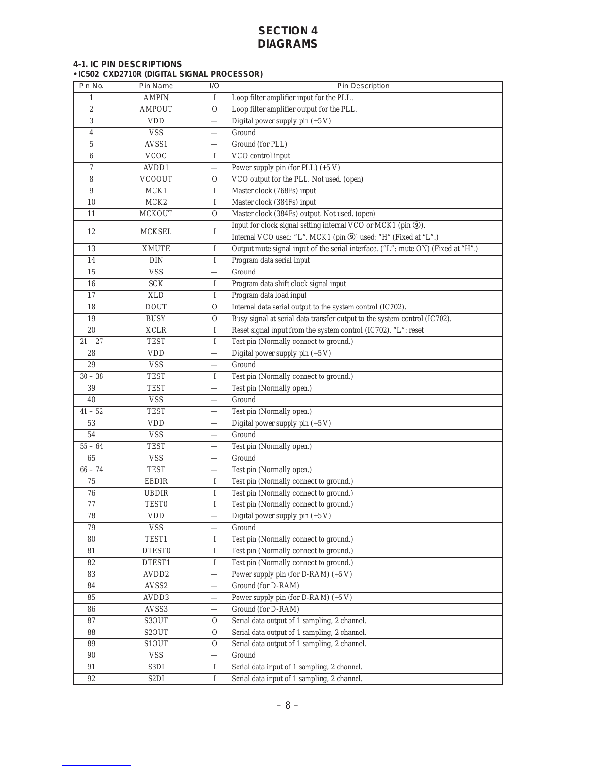
4-1. IC PIN DESCRIPTIONS
• IC502 CXD2710R (DIGITAL SIGNAL PROCESSOR)
Pin No. Pin Name I/O Pin Description
1 AMPIN I Loop filter amplifier input for the PLL.
2 AMPOUT O Loop filter amplifier output for the PLL.
3 VDD — Digital power supply pin (+5 V)
4 VSS — Ground
5 AVSS1 — Ground (for PLL)
6 VCOC I VCO control input
7 AVDD1 — Power supply pin (for PLL) (+5V)
8 VCOOUT O VCO output for the PLL. Not used. (open)
9 MCK1 I Master clock (768Fs) input
10 MCK2 I Master clock (384Fs) input
11 MCKOUT O Master clock (384Fs) output. Not used. (open)
12 MCKSEL I Input for clock signal setting internal VCO or MCK1 (pin 9).
Internal VCO used: “L”, MCK1 (pin 9) used: “H” (Fixed at “L”.)
13 XMUTE I Output mute signal input of the serial interface. (“L”: mute ON) (Fixed at “H”.)
14 DIN I Program data serial input
15 VSS — Ground
16 SCK I Program data shift clock signal input
17 XLD I Program data load input
18 DOUT O Internal data serial output to the system control (IC702).
19 BUSY O Busy signal at serial data transfer output to the system control (IC702).
20 XCLR I Reset signal input from the system control (IC702). “L”: reset
21 – 27 TEST I Test pin (Normally connect to ground.)
28 VDD — Digital power supply pin (+5 V)
29 VSS — Ground
30 – 38 TEST I Test pin (Normally connect to ground.)
39 TEST — Test pin (Normally open.)
40 VSS — Ground
41 – 52 TEST — Test pin (Normally open.)
53 VDD — Digital power supply pin (+5 V)
54 VSS — Ground
55 – 64 TEST — Test pin (Normally open.)
65 VSS — Ground
66 – 74 TEST — Test pin (Normally open.)
75 EBDIR I Test pin (Normally connect to ground.)
76 UBDIR I Test pin (Normally connect to ground.)
77 TEST0 I Test pin (Normally connect to ground.)
78 VDD — Digital power supply pin (+5 V)
79 VSS — Ground
80 TEST1 I Test pin (Normally connect to ground.)
81 DTEST0 I Test pin (Normally connect to ground.)
82 DTEST1 I Test pin (Normally connect to ground.)
83 AVDD2 — Power supply pin (for D-RAM) (+5V)
84 AVSS2 — Ground (for D-RAM)
85 AVDD3 — Power supply pin (for D-RAM) (+5V)
86 AVSS3 — Ground (for D-RAM)
87 S3OUT O Serial data output of 1 sampling, 2 channel.
88 S2OUT O Serial data output of 1 sampling, 2 channel.
89 S1OUT O Serial data output of 1 sampling, 2 channel.
90 VSS — Ground
91 S3DI I Serial data input of 1 sampling, 2 channel.
92 S2DI I Serial data input of 1 sampling, 2 channel.

– 9 –
Pin No. Pin Name I/O Pin Description
93 S1DI I Serial data input of 1 sampling, 2 channel.
94 BCK I Bit clock input of the serial input/output data.
95 LRCK I Sampling clock input of the serial input/output data.
96 LOCK O Error output of the PLL unlock.
97 V O Frequency divider output for the PLL.
98 VAR I PLL phase comparator variable input
99 REF I PLL phase comparator reference input
100 PD O PLL phase comparator charge pump output

– 10 –
• IC503, 504 CXD2711Q (DIGITAL SIGNAL PROCESSOR)
Pin No. Pin Name I/O Pin Description
1 VSS — Ground
2 CRDY O Output of ready signal at serial data transfer to the system control (IC702).
“H”: Ready
3 CCNT I Input of control/data from address bus for the system control (IC702). “L”: data input
4 XCWR I Strobe signal input for data writing from the system control (IC702).
Data are written by a falling edge.
5 XCRD I Strobe signal input for data reading from the system control (IC702). “L”: data read
6 VDD — Power supply pin (+3.3 V)
7 CD0 I/O Two-way data bus (LSB) with the system control (IC702).
8 CD1 I/O
9 CD2 I/O Two-way data bus with the system control (IC702).
10 CD3 I/O
11 VSS — Ground
12 CD4 I/O
13 CD5 I/O Two-way data bus with the system control (IC702).
14 CD6 I/O
15 CD7 I/O Two-way data bus (MSB) with the system control (IC702).
16 VDD — Power supply pin (+3.3 V)
17 XMUTE I Mute control signal input of the audio data. “L”: mute. (Fixed at “H”.)
18 XCCS I Input of chip select signal from address bus. “L”: chip select
19 VSS — Ground
20 MCKO O Master clock signal (18.432 MHz) output. Not used. (open)
21 VSS — Ground
22 XT2O O System clock signal (36.864 MHz) output. Not used. (open)
23 XT2I I System clock signal (36.864 MHz) input
24 VSS — Ground
25 (BIST) — Test pin. Not used. (open)
26 (TCK) — Test pin. Not used. (open)
27 (TDI) — Test pin. Not used. (open)
28 (TENA1) — Test pin. Not used. (open)
29 (TDO) — Test pin. Not used. (open)
30 VST I Not used. (Fixed at “L”.)
31 VSS — Ground
32 XRST I Reset signal input. “L”: reset
33 BCLK I/O Block clock signal input/output. Not used. (open)
34 LRCK I/O L/R sampling clock signal input/output
35 BCK I/O Bit clock signal input/output
36 VSS — Ground
Serial audio data signal input A
37 SIA I IC503: Serial audio data signal input from the digital signal processor (IC502).
IC504: Serial audio data signal input from the digital signal processor (IC502).
Serial audio data signal input B
38 SIB I IC503: Serial audio data signal input from the digital signal processor (IC502).
IC504: Serial audio data signal input from the digital signal processor (IC502).
Serial audio data signal output A
39 SOA O IC503: Serial audio data (high) signal output
IC504: Serial audio data (sub) signal output
Serial audio data signal output B
40 SOB O IC503: Serial audio data (high) signal output
IC504: Serial audio data (low) signal output
41 VSS — Ground
42 – 45 TEST I Test pin. Not used. (Connect to ground.)

– 11 –
Pin No. Pin Name I/O Pin Description
46 VDD — Power supply pin (+3.3 V)
47, 48 TEST I Test pin. Not used. (Connect to ground.)
49 VSS — Ground
50 MD00 I/O IC503: External memory data signal input/output to IC512.
IC504: External memory data signal input/output to IC518.
51 VSS — Ground
52 MD01 I/O IC503: External memory data signal input/output to IC512.
53 MD02 I/O IC504: External memory data signal input/output to IC518.
54 MD03 I/O
55 VSS — Ground
56 MD04 I/O
57 MD05 I/O IC503: External memory data signal input/output to IC512.
58 MD06 I/O IC504: External memory data signal input/output to IC518.
59 MD07 I/O
60 VDD — Power supply pin (+3.3 V)
61 VSS — Ground
62 MD08 I/O
63 MD09 I/O IC503: External memory data signal input/output to IC512.
64 MD10 I/O IC504: External memory data signal input/output to IC518.
65 MD11 I/O
66 VDD — Power supply pin (+3.3 V)
67 MD12 I/O
68 MD13 I/O IC503: External memory data signal input/output to IC512.
69 MD14 I/O IC504: External memory data signal input/output to IC518.
70 MD15 I/O
71 VSS — Ground
72 XRAS O IC503: Row address strobe signal output to external memory (D-RAM: IC512).
IC504: Row address strobe signal output to external memory (D-RAM: IC518).
73 MA09 O Row address strobe signal output to external memory (D-RAM) or address signal
74 MA10 O output to external memory (ROM). Not used. (open)
75 MA11 O
76 VDD — Power supply pin (+3.3 V)
77 MA12 O
78 MA13 O Row address strobe signal output to external memory (D-RAM) or address signal
79 MA14 O output to external memory (ROM). Not used. (open)
80 MA15 O
81 VSS — Ground
82 MA00 O IC503: Address signal output to external memory (D-RAM: IC512).
83 MA01 O IC504: Address signal output to external memory (D-RAM: IC518).
84 VSS — Ground
85 MA02 O IC503: Address signal output to external memory (D-RAM: IC512).
86 MA03 O IC504: Address signal output to external memory (D-RAM: IC518).
87 VDD — Power supply pin (+3.3 V)
88 MA04 O IC503: Address signal output to external memory (D-RAM: IC512).
89 MA05 O IC504: Address signal output to external memory (D-RAM: IC518).
90, 91 VSS — Ground
92 MA06 O IC503: Address signal output to external memory (D-RAM: IC512).
93 MA07 O IC504: Address signal output to external memory (D-RAM: IC518).
94 VSS — Ground
95 MA08 O IC503: Address signal output to external memory (D-RAM: IC512).
IC504: Address signal output to external memory (D-RAM: IC518).
96, 97 MA16, 17 O Address signal output to external memory. Not used. (open)
98 VDD — Power supply pin (+3.3 V)

– 12 –
Pin No. Pin Name I/O Pin Description
99 XMUTE O IC503: Write enable signal output to external memory (D-RAM: IC512).
IC504: Write enable signal output to external memory (D-RAM: IC518).
100 XMODE O IC503: Output enable signal output to external memory (D-RAM: IC512).
IC504: Output enable signal output to external memory (D-RAM: IC518).
101 VSS — Ground
102 XMCS O Chip select output to external memory (ROM). Not used. (open)
103 XCAS O IC503: Column address strobe signal output to external memory (D-RAM: IC512).
IC504: Column address strobe signal output to external memory (D-RAM: IC518).
104 VSS — Ground
105 DEND O Internal operation monitor signal output (DMU END). Not used. (open)
106 VDD — Power supply pin (+3.3V)
107 PEND O Internal operation monitor signal output (PROC END). Not used. (open)
108 ENC0 O Internal operation monitor signal output (BUS ENC0). Not used. (open)
109 ENC1 O Internal operation monitor signal output (BUS ENC1). Not used. (open)
110 ENC2 O Internal operation monitor signal output (BUS ENC2). Not used. (open)
111 VSS — Ground
112 STOP O Internal operation monitor signal output (BUS STOP). Not used. (open)
113 HOLD O Internal operation monitor signal output (BUS HOLD). Not used. (open)
114 OVF O Overflow signal output at the operation. “H”: overflow. Not used. (open)
115 LIM O Fixed/float conversion limiter signal output. “H”: limiter on. Not used. (open)
116 BTIA I Bit signal input A
117 BTIB I Bit signal input B
118 BTOA O Bit signal output A. Not used. (open)
119 BTOB O Bit signal output B. Not used. (open)
120 VDD — Power supply pin (+3.3V)

– 13 –
• IC702 HD6473048SF16 (SYSTEM CONTROL)
Pin No. Pin Name I/O Pin Description
1 VCC — Power supply pin (+5 V)
2 DSPON O System, digital, analog and amplifier remote power supply control signal output.
3 SOUT O Serial data signal output
4 SCKO O Serial clock signal output
5 VCE0 O Not used. (open)
6 2710CE O Program data load output to digatal signal processor (IC502).
7 EE-CKO O Connect to SCK pin of EEPROM (IC705).
8 SP-CE O Serial /Parallel chip enable signal output
9 DSPRDY I Data transfer ready signal input
10 VPP — Not used. (Connect to ground.)
11 VSS — Ground
12 EXT/IO (TX) O UART serial data signal output
13 UNISO O Bus serial data signal output
14 EXT/IO (RX) I UART serial data signal input
15 UNISI I Bus serial data signal input
16 DSPRST O DSP reset control signal output
17 UNICKI I Bus clock signal input
18 – 21 D0 – 3 I/O Two-way data bus to external device. H: Bus off, Back up off.
22 VSS — Ground
23 – 34 D4 – 15 I/O Two-way data bus to external device. H: Bus off, Back up off.
35 VDD — Power supply pin (+5 V)
36 – 43 A0 – 7 O Address bus signal output to external device. H: Bus off, Back up off.
44 VSS — Ground
45 – 56 A8 – 19 O Address bus signal output to external device. H: Bus off, Back up off.
57 VSS — Ground
58 AMUTE O Mute control signal output (Relay mute control)
59 MUT/PW O Mute power signal output
60 — — De-emphasis control signal output. Not used. (open)
61 NC — System clock signal output to external device. Not used. (open)
62 STBY I Hardware standby signal input. Fixed at “H”. (Connect to VDD.)
63 SYSRESET I Reset signal input
64 BU-IN I Back up detect signal input
65 VSS — Ground
66 X-IN I Oscillator (14.7456 MHz) connect pin
67 EX-IN I
68 VDD — Power supply pin (+5 V)
69 AS — Address strobe signal output. Not used. (open)
70 RD O Read signal output
71 HWR O High write signal output
72 LWR O Low write signal output
73 MD0 I Operation mode control signal input. Fixed at “L”. (Connect to ground.)
74, 75 MD1, 2 I Operation mode control signal input. Fixed at “H”. (Connect to VDD.)
76 AVDD — Power supply pin (+5 V)
77 AVREF I Reference voltage signal input
78 DSPBU I DSP BU signal input
79 LOCK (2710) I PLL unlock error detect signal input from digital signal processor (IC502).
80 — — Not used. (Connect to ground.)
81 VOLMAX I Not used. (Connect to ground.)
82 DSPBUSY I Busy signal input
83 SDI-AGC I AGC out signal input. Not used. (Connect to ground.)
84 BU-IN I Back up detect signal input
85 DSPSI (2710) I Data signal input from digital signal processor (IC502).

– 14 –
Pin No. Pin Name I/O Pin Description
86 VSS — Ground
87 BUSON I Bus interface bus on signal input
88 2711-CE O Chip select signal output to digital signal processor (IC503, 504).
89, 90 FROM-CE2, 1 O Chip select signal output for FLASH ROM.
91 BOOT I Forced boot mode detect signal input
92 VSS — Ground
93 LINKOFF O Bus interface link off signal output. “H”: Link off
94 — — Not used. (open)
95 SRD-AGC — Not used. (open)
96 VRCE1 O Chip select signal output to electronic volume (IC303).
97 VRCE2 O Chip select signal output to electronic volume (IC306).
98 VRCE3 O Chip select signal output to electronic volume (IC309).
99 VRCE4 O Chip select signal output to electronic volume (IC312).
100 A20 O Address bus signal output to external device.

BUF
IC102
AMP
IC202
AMP
RELAY
DRIVE
IC110
REF
VOLT
IC111
R-CH
BUF
IC101
R-CH
L
R
L
R
PJ101
-3
-4
-1
-2
GAIN/
BALANCE
PROCESS
IC103, 203
17 9
16
15 12
8
18
7
A/D CONVERTER
IC501
SDATA
LRCK
BCK
A IN L+
A IN L–
CM OUT
RST
MCK
X501
11.288MHz
IC511
IC511
2QC
1
12
11
QB
15 QA
LA CLK
SHCLK
DIGITAL/ANALOG SELECT
IC520
Q916
RY901
14
D
13
OEN B
43
D OUTDATAIN0
LRCK
BCK
FS1
FS2
FS384
ERR
EMPH
PD SEL
DI
LRCI
BCKI
MDT/FST1
40
LRCO
39
1
5
3
17
MDT/FST2
18
ICLK
6
DMUTE
14
MLEN/DEEN
19
BCKO
30
RSTN
6
3
2
5
1
LATCH
IC521
BATT
CHECK
Q910-912
DSP5V
DSP15V
D919
D910
6
3
8
4
79
82
85
78
16
SYSTEM CONTROL
IC702 (1/3)
SP-CE
SCKO
2710CE
SOUT
DSPBU 2
DSPON
DSPSI
DSPBUSY
LOCK
DSPRST
5 6
7
EEPROM
IC705
SCKO
SOUT
MCKDAC
BCK
LRCK
SAMPLE RATE
CONVERTER
IC604
OUTPUT
SECTION
2
EECKO
96
16
17
20
14
92
93
94 89
88
87
95
19
18
LRCK
BCK
S3DI
S2DI
DIN
XCLR
XLD
SCK
LOCK
BUSY
DOUT
S1 OUT
S2 OUT
S3 OUT
DIGITAL
SIGNAL
PROCESSOR
IC502
5
6
7
3
2
15
14
13
17
18
IC507
5V
TO
3V
CONV.
XRST
LRCK
BCK
DATA A
DATA B
DATA C
DSP
SECTION
1
163
23
18
17
26
27
22
20
19
Q601
IC605
IC605
IN1
4
IC605
DIGITAL IN
DEMODULATOR
IC603
1
1
IC601
IC602
MASTER
04
+15V
REG 13
IC903
–15V
REG 23
IC904
+3.3V
REG 13
IC905
D912
D914
D913
DSP +15V
DSP –15V
DSP +3.3V
U +5V
DSP +5V ON/OFF
DRIVE
+5V
REG
POWER
CONTROL
REMOTE
+B
+B
Q914
T901
10
12
OUT
3VFB
VCC
DC/DC
CONVERTER
IC902
Q903, 906
Q907,908
RELAY
+B
Q917
REG
Q913
RL +B
+B(A)
+B
D905
+B
CN901
REM OUT
+B
Q909,918
+B
ER +5V +5V
REG
IC950
DSP +15V
ER –5V –5V
REG
IC951
DSP –15V
Signal path
: ANALOG
: DIGITAL
CHANGER
ANALOG IN
MASTER
CHANGER
DIGITAL IN
– 15 – – 16 –
XDP-4000X
4-2. BLOCK DIAGRAM — INPUT SECTION —
(Page 17)
(Page 19)

XDP-4000X
– 17 – – 18 –
4-3. BLOCK DIAGRAM — DSP SECTION —
9
DSPRDY
71
HWR
70
RD
2711-CE
LWR
D0-15
A0-20
SYSTEM CONTROL
IC702 (2/3)
14
12
BUS INTERFACE
IC701
1
SW
12
2 13 87
15
88
139
4 11 17
10
6
52
41
8
7
MASTER
CN701
63
52
41
8
7
CN702
63
7 8
93
63
67
66
72
64
84
Q701
+B (A)
U+5V
Q702
CN707
RX
TX
(SERIAL I/O)
EXT/IO (TX)
EXT/IO (RX)
BUSON
UNISI
UNISO
UNICKI
LINK OFF
SYSRESET
EX IN
X701
14.74MHz X IN
BU IN
BU IN
RESET 21
IC901 IC706
BUF
BATT
CHECK
Q901, 902
+B
D903
D902
IC706
36-43
45-56
100
18-21
23-34 D0-15
FLASH ROM
IC703
46 11 43 44
31-34
38-41
A0-20
3-10 14-21
2
22
2
7
3
4
5
6
18
13
17
16
15
14
IC513
5V
&
3V
CONV.
5V
TO
3V
CONV.
IC506
OR
GATE
A0
A20
A1
IC510
IC508
XRST
DATA C
DATA B
DATA A
BCK
LRCK
INPUT
SECTION
135
34
37
38
2 32 3 4 5 18 23
99 72103100
40
39
LRCK
BCK
SIA
SIB
50,52-54,56-59
62-65,67-70
82,83,85
86,88,89
92,93,95
DSP
IC503
CRDY
XRST
CCNT
XCWR
XCRD
XCCS
XMODE
XCAS
XMUTE
XRAS
XT21
46 11 43 44
31-34
38-41
A20
CE
OE
WE
A20
CE
OE
WE
FLASH ROM
IC704
2 32 3 4 5 18 23
100 103 99 72
39
40
7-10
12-15
CRDY
XRST
CCNT
XCWR
XCRD
XCCS
CD0-7
XT21
37
38
35
34 LRCK
BCK
SIB
SIA
IC509 IC509
X502
33.86MHz
50,52-54
56-59,62-65
67-70
82,83,85
86,88,89
92,93,95
D0-15
A0-8
29 30 31 15 16
2-5,7-10
35-38,40-43
18-24
24-28
OE
UCAS
LCAS
WE
RAS
DRAM
IC518
D0-15
A0-8
29 30 31 15 16
2-5,7-10
35-38,40-43
18-21
24-28
OE
UCAS
LCAS
WE
RAS
DRAM
IC512
XMODE
XCAS
XMUTE
XRAS
SOA
SOB
4
5
SOA
SOB 3
2 18
17
15
16
7-10
12-15
CD0-7
IC514
3V
TO
5V
CONV.
DATA (HIGH)
DATA (M-H)
DATA (SUB)
DATA (M-L)
OUTPUT
SECTION
3
04
FROM CE1
FROM-CE2 89
90
IC508
A1-20
D8-15D0-7
D8-15
DSP
IC504
F0-7
A0-15
A0-20
CHANGER
BUS
CONTROL
Signal path
: ANALOG
: DIGITAL
(Page 19)
(Page 16)

INPUT
SECTION
2
DSP
SECTION
3
SCKO
SOUT
LRCK
MCKDAC
BCK
D/A CONVERTER
IC530
7
14
LRCK
8MCLK
9SCLK
10 SDATA
AO/R+
13
AO/R–
18
AO/L+
17
AO/L–
LPF AMP
R-CH
IC302 IC401
AMP
IC304
THE SAME AS ABOVE BLOCK DIAGRAM
CS
SDI
SCLK
AIR AOUTR
2
3
6
9 11
ELECTRONIC VOLUME
IC303
Q301
MUTE
CONTROL
POWER
CONTROL
Q952-954Q950, 951
96
97
98
99
59
58
AMUTE
MUT/PW
VRCE1
VRCE2
VRCE3
VRCE4
SYSTEM CONTROL
IC702 (3/3)
R-CH
–2
–1
PJ301
L
R
C
R-CH
–4
–3
PJ301
L
R
R-CH
–2
–1
PJ302
L
R
R-CH
–4
–3
PJ302
L
R
04
DATA (HIGH)
DATA (M-H)
DATA (M-L)
DATA (SUB)
Signal path
: ANALOG
: DIGITAL
+B
D
A
B
LINE OUT
– 19 – – 20 –
XDP-4000X
4-4. BLOCK DIAGRAM — OUTPUT SECTION —
(Page 16)
(Page 18)

– 21 – – 22 –
4-5. PRINTEDWIRING BOARD — MAIN SECTION —
IC508 J-15
IC509 J-16
IC510 L-10
IC511 I-17
(IC512) L-13
IC513 N-10
IC514 I-18
(IC518) L-17
IC520 H-16
IC521 F-10
IC522 H-17
(IC601) A-10
(IC602) A-11
IC603 C-10
IC604 D-8
IC605 C-8
IC701 C-7
IC702 G-10
IC703 G-7
IC704 F-7
IC705 D-11
IC706 H-11
IC901 H-4
IC902 L-2
(IC903) J-6
(IC904) I-6
IC905 K-7
IC950 H-15
IC951 H-14
Q301 B-15
Q302 B-15
Q303 B-16
Q304 B-17
Q305 B-17
Q306 B-18
Q307 B-18
Q308 B-18
Q601 C-8
Q701 C-7
Q702 D-6
Q901 G-3
Q902 G-3
Q903 G-3
Q906 G-2
Q907 D-4
Q908 E-4
(Q909) F-4
Q910 H-2
Q911 G-2
Q912 H-3
(Q913) C-4
(Q914) J-2
Q916 E-12
Q917 B-6
Q918 G-4
Q950 E-14
Q951 D-14
Q952 D-13
Q953 C-14
Q954 D-13
Q955 C-14
D100 B-12
D101 B-11
D102 B-13
D104 B-12
D105 B-11
D106 B-13
D200 B-12
D201 B-13
D202 B-14
D204 B-12
D205 B-12
D206 C-14
D701 C-7
D702 C-7
D703 B-7
D704 A-7
D707 D-8
D901 D-2
D902 F-3
D903 F-3
D906 F-4
D907 G-5
D908 G-4
(D909) E-12
D910 H-3
D911 E-5
(D912) J-4
(D913) I-3
D914 K-4
(D915) I-3
D916 B-3
D919 H-2
D922 K-3
D923 K-2
(D924) I-7
(D925) I-6
D950 E-13
IC101 C-13
IC102 C-12
IC103 F-13
IC110 D-12
IC111 F-12
IC202 C-12
IC203 F-13
IC303 D-14
IC304 C-14
IC306 D-16
IC307 C-15
IC309 D-17
IC310 C-17
IC312 D-18
IC313 C-18
IC401 F-15
IC405 F-16
IC408 F-17
IC411 F-18
IC501 H-13
IC502 M-7
IC503 L-13
IC504 L-17
IC506 L-9
IC507 M-10
• Semiconductor Location
Ref.No. Location
( ) : SIDE B
Ref.No. Location
XDP-4000X
Note:
•X: parts extracted from the component side.
•®:Through hole.
•b: Pattern from the side which enables seeing.
(The other layer’s patterns are not indicated.)
Caution:
Pattern face side: Partsonthepattern faceside seenfromthe
(Side B) pattern face are indicated.
Parts face side: Parts on the parts face side seen from the
(Side A) parts face are indicated.

XDP-4000X
– 23 – – 24 –
(Page 37)
(Page 35)
(Page 38)
(Page 35)
(Page 35)

XDP-4000X
– 25 – – 26 –
4-6. SCHEMATIC DIAGRAM — MAIN SECTION (1/4) — • Refer to page 32 for Note and refer to page 39 for IC Block Diagrams.
(Page 29)
(Page 27)
Other manuals for XDP-4000X Operating Instructions (primary...
3
Table of contents
Other Sony Amplifier manuals

Sony
Sony XM-3001SXD - Stereo Power Amplifier User manual

Sony
Sony EXM-302 User manual

Sony
Sony TA-AV431 User manual

Sony
Sony XM-404EQX User manual

Sony
Sony TA-AV581 User manual

Sony
Sony TA-E9000ES - Stereo Preamplifier Quick start guide

Sony
Sony TA-SB500WR User manual

Sony
Sony XM-604EQX Marketing Specifications User manual

Sony
Sony XM-D1000P5 Marketing Specifications User manual

Sony
Sony XM-GS400 User manual