Sony HCD-S20 User manual

SERVICE MANUAL
Sony Corporation
Published by Sony Techno Create Corporation
HCD-S20
SPECIFICATIONS
COMPACT DISC RECEIVER
9-893-739-01
2013D33-1
© 2013.04
E Model
Ver. 1.0 2013.04
• HCD-S20 is compact disc receiver in CMT-S20.
Model Name Using Similar Mechanism NEW
Mechanism Type TDL-5
Amplier section
Power output (rated): 4 watts + 4 watts
(8 ohms at 1 kHz, 1% THD)
Continuous RMS power output (reference):
5 watts + 5 watts (8 ohms at 1 kHz, 10% THD)
Input
AUDIO IN (stereo mini jack): Sensitivity 1 V,
impedance 50 kilohms
Outputs
SPEAKERS: Accepts impedance of 8 ohms
CD player section
System: Compact disc and digital audio system
Laser Diode Properties
Emission Duration: Continuous
Laser Output*: Less than 44.6μW
* This output is the value measurement at a distance of
200mm from the objective lens surface on the Optical
Pick-up Block with 7mm aperture.
Frequency response: 20 Hz 20 kHz
Signal-to-noise ratio: More than 90 dB
Dynamic range: More than 90 dB
Tuner section
FM stereo, FM superheterodyne tuner
Antenna: FM lead antenna
Tuning range: 87.5 MHz 108.0 MHz (50 kHz
step)
USB section
(USB) port: Type A, maximum current 500 mA
Supported audio formats
Supported bit rate:
MP3 (MPEG 1 Audio Layer-3): 32 kbps
320 kbps, VBR
WMA: 32 kbps 192 kbps, VBR
Sampling frequencies:
MP3 (MPEG 1 Audio Layer-3): 32/44.1/48 kHz
WMA: 44.1 kHz
General
Except Korean model:
Power requirements: AC 120 V 240 V, 50/60 Hz
Korean model:
Power requirements: AC 220 V 240 V, 50/60 Hz
Power consumption: 18 watts
Dimensions (W/H/D, including largest
protrusions) (excl. speakers):
Approx. 170 mm × 133 mm × 240 mm
Mass (excl. speakers): Approx. 1.3 kg
Quantity of the main unit: 1 piece
Design and specifications are subject to change
without notice.
Standby power consumption: 0.5 W
Halogena ted flame retardants are not used in
the certain printed wiring boards.

HCD-S20
2
1. SERVICING NOTES ............................................. 3
2. DISASSEMBLY
2-1. Disassembly Flow........................................................... 7
2-2. Top Cover Assy S20........................................................ 7
2-3. Power Cord (AC1), Rear Panel....................................... 8
2-4. CD Door (S20)................................................................ 8
2-5. Loader (TDL-5) & OPU Assy (CDM1).......................... 9
2-6. Front Panel Block ........................................................... 9
2-7. VFD Board...................................................................... 10
2-8. USB Board...................................................................... 10
2-9. MAIN Board ................................................................... 11
2-10. POWER Board................................................................ 11
3. TEST MODE ............................................................ 12
4. ELECTRICAL CHECK ......................................... 13
5. TROUBLESHOOTING .......................................... 14
6. DIAGRAMS
6-1. Block Diagram................................................................ 16
6-2. Board Component Diagram (1/3) ................................... 17
6-3. Board Component Diagram (2/3) ................................... 18
6-4. Board Component Diagram (3/3) ................................... 19
6-5. Printed Wiring Board - MAIN Board -........................... 21
6-6. Schematic Diagram - MAIN Board (1/6) -..................... 22
6-7. Schematic Diagram - MAIN Board (2/6) -..................... 23
6-8. Schematic Diagram - MAIN Board (3/6) -..................... 24
6-9. Schematic Diagram - MAIN Board (4/6) -..................... 25
6-10. Schematic Diagram - MAIN Board (5/6) -..................... 26
6-11. Schematic Diagram - MAIN Board (6/6) -..................... 27
6-12. Printed Wiring Board - USB Board -.............................. 28
6-13. Schematic Diagram - USB Board -................................. 29
6-14. Printed Wiring Board - VFD Board -.............................. 30
6-15. Schematic Diagram - VFD Board - ................................ 31
6-16. Printed Wiring Board - KEY Board -.............................. 32
6-17. Schematic Diagram - KEY Board - ................................ 33
6-18. Schematic Diagram - POWER Board - .......................... 34
6-19. Printed Wiring Board - POWER Board -........................ 35
7. EXPLODED VIEWS
7-1. Top Cover Section........................................................... 36
7-2. Chassis Section ............................................................... 37
7-3. Front Panel Section......................................................... 38
TABLE OF CONTENTS
NOTES ON CHIP COMPONENT REPLACEMENT
• Never reuse a disconnected chip component.
• Notice that the minus side of a tantalum capacitor may be dam-
aged by heat.
SAFETY-RELATED COMPONENT WARNING!
COMPONENTS IDENTIFIED BY MARK 0OR DOTTED LINE
WITH MARK 0ON THE SCHEMATIC DIAGRAMS AND IN
THE PARTS LIST ARE CRITICAL TO SAFE OPERATION.
REPLACE THESE COMPONENTS WITH SONY PARTS
WHOSE PART NUMBERS APPEAR AS SHOWN IN THIS
MANUAL OR IN SUPPLEMENTS PUBLISHED BY SONY.
CAUTION
Use of controls or adjustments or performance of procedures
other than those specified herein may result in hazardous radia-
tion exposure.

HCD-S20
3
SECTION 1
SERVICING NOTES
NOTES ON HANDLING THE OPTICAL PICK-UP
BLOCK OR BASE UNIT
The laser diode in the optical pick-up block may suffer electro-
static break-down because of the potential difference generated by
the charged electrostatic load, etc. on clothing and the human body.
During repair, pay attention to electrostatic break-down and also
use the procedure in the printed matter which is included in the
repair parts.
The flexible board is easily damaged and should be handled with
care.
NOTES ON LASER DIODE EMISSION CHECK
The laser beam on this model is concentrated so as to be focused
on the disc reflective surface by the objective lens in the optical
pickup block. Therefore, when checking the laser diode emission,
observe from more than 30 cm away from the objective lens.
UNLEADED SOLDER
Boards requiring use of unleaded solder are printed with the lead-
free mark (LF) indicating the solder contains no lead.
(Caution: Some printed circuit boards may not come printed with
the lead free mark due to their particular size)
: LEAD FREE MARK
Unleaded solder has the following characteristics.
• Unleaded solder melts at a temperature about 40 °C higher
than ordinary solder.
Ordinary soldering irons can be used but the iron tip has to be
applied to the solder joint for a slightly longer time.
Soldering irons using a temperature regulator should be set to
about 350 °C.
Caution: The printed pattern (copper foil) may peel away if
the heated tip is applied for too long, so be careful!
• Strong viscosity
Unleaded solder is more viscous (sticky, less prone to flow)
than ordinary solder so use caution not to let solder bridges
occur such as on IC pins, etc.
• Usable with ordinary solder
It is best to use only unleaded solder but unleaded solder may
also be added to ordinary solder.
ABOUT PART REPAIR OF EACH BOARD
The part that mounted on each board cannot exchange. When the
mounted part is damaged, exchange with the complete mounted
board or part including complete mounted board.
Printed wiring board and schematic diagram that have been de-
scribed on this service manual are for reference.
TEST DISCS
Use following TEST DISC (for CD) when this unit confirms the
operation and checks it.
Part No. Description
3-702-101-01 DISC (YEDS-18), TEST
4-225-203-01 DISC (PATD-012), TEST
RELEASING THE DISC TRAY LOCK
The disc tray lock function for the antitheft of sample disc in the
shop is equipped.
Releasing Procedure:
1. Press the [?/1] button to turn the power on.
2. Press two buttons of the [x] on the remote commander and
[Z] on the main unit simultaneously for five seconds.
3. The message “UNLOCKED” is displayed on the fluorescent
indicator tube and the disc tray is unlocked.
Note: When “LOCKED” is displayed, the disc tray lock is not released by
turning power on/off with the [?/1] button.
CAPACITOR ELECTRICAL DISCHARGE PROCESSING
When checking the board, the electrical discharge is necessary for
the electric shock prevention.
Connect the resistor to both ends of respective capacitors.
• POWER Board
CE501, CE502, CE534
– POWER Board (Conductor Side) –
800 :/2 W
(for CE501)
800 :/2 W
(for CE502)
800 :/2 W
(for CE534)

HCD-S20
4
MODEL IDENTIFICATION
Distinguish by model number label stuck on the rear side of a main unit.
MODEL NUMBER LABEL
05/2013
110 – 240V AC area in E model (E32) Singapore model (SP1)
Saudi Arabia model (EA3) Argentina model (AR2)
Mexican model (MX2) Korean model (KR2)

HCD-S20
5
COMPONENT REPAIR GUIDE
1. No Display When You Turn The Main Unit ON
When you plug power cord and turn the main unit on, VFD won’t
display.
Procedure:
1. Check POWER board have +12V DC output.
2. Check MAIN board output voltage +5V and −24V from U2 on
the MAIN board.
If output +5V or −24V is not normal, check the working status
of U2 on the MAIN board.
3. Check output voltage 3.3 from U3 on the MAIN board.
If output +3.3V is not normal, check the working status of U3
on the MAIN board.
4. Check waveform of Y3 on the MAIN board , the waveform of
Y3 on the MAIN board sine wave.
If waveform of Y3 on the MAIN board is not normal, check Y3
on the MAIN board.
2. When You Plug Power Cord and Turn The Main Unit
ON, The Main Unit Won’t Have Sound
Procedure:
1. Check U5 on the MAIN board and its peripheral circuit.
2. Check if output voltage +3.3V from pin 32, pin 54, pin 70, pin
72, pin 78 and pin 83 of U5 on the MAIN board.
If output voltage +3.3V is not normal, check +3.3V power cir-
cuit of MAIN board.
3. Check if output voltage +1.2V from pin 10, pin 77 and pin 86
of U5 on the MAIN board.
If output voltage +1.2V is not normal, check +1.2V power cir-
cuit of MAIN board.
4. Check if oscillating frequency 27 MHz of Y10 crystal on the
MAIN board is normal.
If oscillating frequency 27 MHz is not normal, check if Y10 on
the MAIN board and its peripheral circuit is in failure.
5. Check if the status of U17 and U25 on the MAIN board work
well, the normal status of pin 27 of U25 on the MAIN board is
sine wave with frequency 11.0592 MHz. And pin 23 of U25 on
the MAIN board is high in normal status.
If pin 27 of U25 on the MAIN board wave is not normal, check
if U17 and U25 on the MAIN board and its peripheral circuit is
in failure.
3. When You Plug Power Cord and Turn The Main Unit
ON, The Main Unit Won’t Read Disc Normal
Procedure:
1. Check U5 on the MAIN board signal and its peripheral circuit,
and check output voltage +3.3V from pin 8 of U6 on the MAIN
board is normal.
If output voltage +3.3V is not normal, check +3.3V power cir-
cuit of MAIN board.
2. Check every signal connected between U5 and U6 on the
MAIN board, especially including DATA, CLK and CS signal.
If DATA, CLK and CS signal is not normal output, check if U6
on the MAIN board is in failure.
3. Check if output voltage +5V from pin 8, pin 19 and pin 21 U7
on the MAIN board is normal.
If output voltage +5V is not normal, check +5V power circuit
of MAIN board.
4. Check every signal connected between U5 and U7 on the
MAIN board, especially including F+, F−, T+, T−, SP+, SP−,
SL+ and SL−signal to drive MD.
If F+, F−, T+, T−, SP+, SP−, SL+ and SL−signal is not nor-
mally output, check if U7 on the MAIN board is in failure.
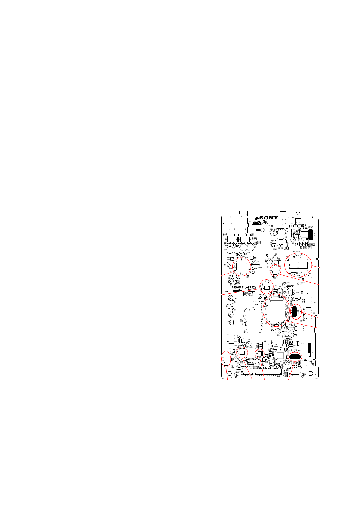
Checking Location:
– MAIN Board (Component Side) –
+12V power from
POWER board
U2 U3 Y3
U5
Y10
U1
7
U7
U25
U6

HCD-S20
6
HOW TO EJECT THE DISC WHEN POWER SWITCH TURN OFF
SERVICE POSITION
3Pull out the disc tray.
2Turn the traverse gear in
the direction of an arrow.
1Refer to “SECTION 2. DISASSEMBLY” (page 7), remove the top cover assy S20 and the rear panel block from the unit.
bottom side
top side
– Rear view –
– Rear view –
MAIN board
POWER board
VFD board
KEY board
USB board
loader (TDL-5) & OPU assy
(CDM1)

HCD-S20
7
SECTION 2
DISASSEMBLY
• This set can be disassembled in the order shown below.
2-1. DISASSEMBLY FLOW
Note: Follow the disassembly procedure in the numerical order given.
2-2. TOP COVER ASSY S20
(Page 7)
SET
2-3. POWER CORD (AC1), REAR PANEL
(Page 8)
2-4. CD DOOR (S20)
(Page 8)
2-6. FRONT PANEL BLOCK
(Page 9)
2-9. MAIN BOARD
(Page 11)
2-7. VFD BOARD
(Page 10)
2-8. USB BOARD
(Page 10)
2-10. POWER BOARD
(Page 11)
2-5. LOADER (TDL-5) & OPU ASSY (CDM1)
(Page 9)
1three screws (2)
2Remove the top cover assy S20
in the direction of an arrow.
5top cover assy S20
3four claws
4connector
(XP1)
3four claws
3two claws
3three claws

HCD-S20
8
2-3. POWER CORD (AC1), REAR PANEL
2-4. CD DOOR (S20)
2claw
2claw
2claw
6rear panel
2claw
1screw (3)
3RZHUFRUGVHWWLQJ
–5HDUSDQHOEORFNOHIWYLHZ–
3Remove the rear panel block
in the direction of an arrow.
bottom side
4power cord connector
(CN503)
5power cord
(AC1)
–5HDUYLHZ–
top side
Note: When installing the power cord (AC1),
Check the direction of connector.
3four claws
4CD door (S20)
2Pull out the disc tray.
1Turn the traverse gear in
the direction of an arrow.
bottom side
top side
– Rear view –
– Rear view –

HCD-S20
9
2-5. LOADER (TDL-5) & OPU ASSY (CDM1)
1Solder the short-land.
Note 2: When assembling the loader (TDL-5) &
OPU assy (CDM1), remove the solder of
short-land after connecting all flexible flat
cable and connector.
2screws (3)
2screws (3)
5connector
(XP3)
4flexible flat cable
(XP2)
7loader (TDL-5) & OPU assy
(CDM1)
3Remove the loader (TDL-5) & OPU
assy in the direction of an arrow. 6connector (XP4)
Note 3: Since the wire is very thin, it is easy to cut.
When disconnecting, do it while holding the
connector part.
.
Note 1: Before disconnecting the flexible flat cable of the loader (TDL-5) & OPU assy (CDM1), solder the short-land.
– Bottom view –
Note 4: The wire is soldered to the
terminal of the switch.
Be careful so that not cut
or bend the terminal.
2-6. FRONT PANEL BLOCK
4six claws
5front panel block
– Rear right view –
3connector
(XP12)
1connector
(XP6)
2connector
(XP9)
Wire setting
Wire from USB board is upper.
Wire from VFD board is lower.
– Rear view –
Note 2: These connectors have the same number of pins.
When connecting, be careful not to mistake.
VFD board
chassis
front panel block
Note 1: When installing the front panel
block, be careful not to bite the
wire at the chassis.

HCD-S20
10
2-7. VFD BOARD
2-8. USB BOARD
1three claws
WireVeWWiQJ
2VFD board
VFD board
–)rRQWSDQeOEORFNreDrYieZ–
2two screws
(BVTP2.6)
2screw (1)
2screw (1)
3earth plate
5USB board
USB board
WireVeWWiQJ
4six claws
1VOL knob
–)rRQWSDQeOEORFNreDrYieZ–

HCD-S20
11
2-9. MAIN BOARD
2-10. POWER BOARD
4connector
(XP12)
6MAIN board
5screw (3)
A
A
1connector
(CON2)
2connector
(XP6)
3connector
(XP9)
Wire from USB board is upper.
Wire from VFD board is lower.
Note: These connectors have the
same number of pins.
When connecting, be careful
not to mistake.
– Rear view –
– Rear view –
:ire VeWWiQJ
3POWER board
1connector
(CON2)
2screw (3)
2screw (3)
– Rear view –

HCD-S20
12
SECTION 3
TEST MODE
SOFTWARE VERSION
It can confirm the software version.
Procedure:
1. Press the [?/1] button to turn the power on.
2. Press the [Z] button to open the disc tray.
3. Press the button on the remote commander as following order.
[CLEAR] →[B] →[RETURN]
(Displayed values in the following figure are example)
M20F3P15
Screen display
MCU IC
Software version
Software
difference
MPEG IC
Software version
Software Difference
Destination Display Specifications
110 – 240V AC area in
E model F3
FM 50 kHz step, no RDS,
Tuner output level 2.2 dB,
12 hours display
Saudi Arabia model F4
FM 50 kHz step, no RDS,
Tuner output level 4.2 dB,
12 hours display
Mexican model F4
FM 50 kHz step, no RDS,
Tuner output level 4.2 dB,
12 hours display
Singapore model F4
FM 50 kHz step, no RDS,
Tuner output level 4.2 dB,
12 hours display
Argentina model F3
FM 50 kHz step, no RDS,
Tuner output level 2.2 dB,
12 hours display
Korean model F6
FM 50 kHz step, no RDS,
Tuner output level 7.2 dB,
12 hours display
Releasing method:
Press the [Z] button to close the disc tray or press the [?/1] button
to turn the power off.
FACTORY RESET
It can clears all data including preset data stored in the memory to
initial conditions. Execute this mode when returning the this unit
to the customer.
Procedure:
1. Press the [?/1] button to turn the power on.
2. Press two buttons of the [x] on the remote commander and
[EQ] on the main unit simultaneously for five seconds.
3. The message “RESET OK is displayed on the fluorescent indi-
cator tube, then returns to the normal mode.
TRAY LOCK
It can be unable to take sample disc out of disc tray in the shop.
Procedure:
1. Press the [?/1] button to turn the power on.
2. Press the [Z] button to open the disc tray.
3. Set a disc on the disc tray.
4. Press the [Z] button to close the disc tray.
5. Press two buttons of the [x] on the remote commander and [Z]
on the main unit simultaneously for five seconds.
6. The message “LOCKED” is displayed on the fluorescent indi-
cator tube and the disc tray is locked.
(Even if pressing the [Z] button, the message “LOCKED” is
displayed on the fluorescent indicator tube and the disc tray is
locked)
Releasing method:
1. Press two buttons of the [x] on the remote commander and [Z]
on the main unit simultaneously for five seconds.
2. The message “UNLOCKED” is displayed on the fluorescent
indicator tube and the disc tray is unlocked.
PANEL TEST
It can confirm the fluorescent indicator tube.
Procedure:
1. Press the [?/1] button to turn the power on.
2. Press two buttons of the [x] on the remote commander and [x/
CANCEL] on the main unit simultaneously for five seconds.
3. All segments on the fluorescent indicator tube light up.
Screen display
Releasing method:
Press two buttons of the [x] on the remote commander and [x/
CANCEL] on the main unit simultaneously for five seconds or
press the [?/1] button to turn the power off.

HCD-S20
13
SECTION 4
ELECTRICAL CHECK
CD SECTION
Note:
1. CD block is basically constructed to operate without adjustment.
2. Use YEDS-18 disc (Part No. 3-702-101-01) unless otherwise indicat-
ed.
3. Use an oscilloscope with more than 10 Mimpedance.
4. Clean the object lens by an applicator with neutral detergent when the
signal level is low than specified value with the following check.
RF SIGNAL CHECK
+
–
MAIN board
TP66 (PUHRF)
TP46 (VREF1)
oscilloscope
(DC range)
Procedure:
1. Connect the oscilloscope to TP66 (PUHRF) and TP46
(VREF1) on the MAIN board.
2. Press the [?/1] button to turn the power on.
3. Press the [FUNCTION] button to turn the CD function.
4. Set the disc (YEDS-18) in the main unit and press the [u]
button to playback.
5. Confirm that oscilloscope waveform is as shown in the figure
below. (eye pattern)
A good eye pattern means that the diamond shape () in the
center of the waveform can be clearly distinguished.
VOLT/DIV: 200 m
V
TIME/DIV: 400 ns
level: 1.2 ± 0.2 Vp-p
Connection Location:
– MAIN Board (Conductor Side) –
TP46
(VREF1)
TP66
(PUHRF)
TP46
(VREF1)
TP66
(PUHRF)

HCD-S20
14
1. Operation Check Flow
Power is turned on.
Check if the CD tray
can open/close.
Check if the voltage at pin 1 of CON2 on the
POWER board is +12V.
Exchange the VFD and check if the power is
turned on.
NG
OK
OK
Check if the USB
playback is OK.
OK
OK
NG Exchange the POWER board.
NG Exchange the MAIN board.
Check if the wire is inserted to XP4 on the
MAIN board.
Check if the wire is inserted to XP3 and the
FFC is inserted to XP2 on the MAIN board.
NG
OK
Check if the CD
playback is OK.
OK
Check if FM reception
and AUDIO IN
function is OK.
OK
No problem.
NG
NG Insert the wire.
NG Insert the wire and the FFC.
Check if the signal at TP66 on the MAIN board
is OK.
OK
Check if the wire to XP6 on the MAIN board is
inserted.
NG
NG
NG Insert the wire to XP6.
Exchange the MAIN board.
OK
Exchange the MAIN board.
OK
NG Exchange the LOADER (TDL-5) & OPU ASSY
(CDM1).
SECTION 5
TROUBLESHOOTING

HCD-S20
HCD-S20
1515
2. Flow When “OVER CURRENT” is Displayed
“OVER CURRENT” is
displayed on the VFD.
Disconnect the USB board and check if the
display persists.
Exchange the MAIN board.
OK
NG Exchange the USB board.
3. Flow When “PROTECT” is Displayed
“PROTECT” is
displayed on the VFD.
Check the if the voltage at pin 1 of CON2 on
the POWER board is +12V.
Exchange the MAIN board.
OK
NG Exchange the POWER board.
4. Flow When “LOCKED” is Displayed
“LOCKED” is displayed
on the VFD when
[OPEN/CLOSE] button
is pressed.
Hold down [STOP] button of remote commander and
[OPEN/CLOSE] button of main unit for 5 seconds.
And the check if “UNLOCKED” is displayed on the
VFD.
NG Exchange the POWER board.

HCD-S20
HCD-S20
1616
SECTION 6
DIAGRAMS
6-1. BLOCK DIAGRAM
MCU
M0516
MPEG Decoder
SPHE8104-MW
AMP
STA339BWS
SDRAM
M12L64164
FLASH
EN25T80
LOADER
TDM-5+IM OPU
Moto driver IC
CD5890
ADC
AK5358A
AUDIO
SW IC
74HC4052 UART
I2S
3.3V
1.2V
IR
IRR006
KEY
I2C
VFD Display
FV935ND
L/R
I2S
VFD Driver
S16312
I2C
USB
USB005
RTC
PCF8563
I2C
AUX IN
EAR004
FM
RZ5B705
L/R
L/R
12V
STB_3.3V
Power
Board
DC DC
EUP3482A
110V-
220V~
AC IN
MOS
ON/OFF 12V
LDO
G9091
MOS
ON/OFF
5V LDO
G9091 FM3.3V
POWER
OTHER
CONTROL
DATA
SPI
IR
SPI
ADC
5W*2
I/O
USB
5V
-24V

HCD-S20
HCD-S20
1717
6-2. BOARD COMPONENT DIAGRAM (1/3)
VFD_DAT
USB BD
ADC_KEY1
ADC_KEY2
FL-
FR+
FR-
AMP
14
TDL-5+DOREE)
DVD LOADER
8ohm
XS301
VFD DISPLAY+CS16312
VOL-
VOL+
POWER KEY
GND
4PIN*2.0
ST339BWS
4PIN*2.0
12 1
12PIN/2.0
XP12
12
1
XS
12PIN
FL+
XP6
SPI
FLASH
14
MAIN+AMP BOARD
4PIN*2.0
SPHE8104MW
ADC
64M
SDRAM
AK5358
XP9
VFD_CS
GND
12V
VFD_CLK
-24V
INSW
GND
SL+
SL-
GND
HOMESW
SP+
SP-
TUNER L/R Out
IR
GND
GND
POWER_BOARD
4PIN/2.5mm
4
1
4
1
4PIN/2.0mm
XS1
GND
12V
12V
GND
KEY BD
3PIN*2.0
4PIN*2.0
24PIN*0.5
XP2
1
XP3
6PIN*2.0
6
1
5PIN*2.0
5
1
XP4
4
8ohm
74HC4053
AUDIO IN
TUNER
AUDIO IN L/R
5890
MOTER
DRIVER
IIS DATA IN
SPI
IIS DATA OUT
MCU
M0516
IIC
UART
IIC
RTC
PCF8563
IIC
5V
1
3
ADC_KEY1
ADC_KEY2
GND
XP1
USB

HCD-S20
HCD-S20
1818
6-3. BOARD COMPONENT DIAGRAM (2/3)
Motor Contr
5PIN*2.0 6PIN*2.0
6
1
5
1
SPI
FLASH
24PIN*0.5 XP3
1
24
OPU Signal
USB
14
5890
MOTER
DRIVER
MOTR CTR
Feed Back
ADC
AK5358
AMP
MCU And MPEG Commuication
SPK2.0 OUT
+12V
LDO STB3.3V
+12V
3.3V
1.2V
3.3V
I2S In Signal
4PIN*2.5
XS1
I2S IN Signal
VFD Board Control
12PIN*2.0
SPHE8104MW
M0516
MCU
XP12
Tunner
Motor Contr
EUP3482A
+5V
I2C Signal
74HC4052
Audio IN
64M
SDRAM
L/R
L/R
LDO
FM3.3V
5V
I2C Signal
4PIN*2.0
XP9
USB Board Control(Volume)
Main Board PCB LAYOUT

HCD-S20
HCD-S20
1919
6-4. BOARD COMPONENT DIAGRAM (3/3)
LDO G9091
VBUS SWITCH
MCU3V3 MCU_M516
MO_VCC
MOS USB
SWITCH
MCU GPIO
ADC_AK5358A
MOTO DRIVER IC 5890
OPU
DC-DC
5890 DVCC3 FLASH
SRV33 SDRAM
RFV33
DVCC3
OPU
SUNPLUS 8104MW
DC-DC
5890
ADC_AK5358A
V12
+5V
EUP3482APOWER BOARD +12V
VFD
-24V
6mA
DVCC3
+5V
0.5A
15mA
MAX 2.3A
12V
STA339BWS
B+ SWITCH AMP_VCC
0.84A
160mA
35mA
SUNPLUS 8104MW
650mA
18mA
25mA
500mA
74HC4052
50mA
A5V

HCD-S20
HCD-S20
2020
For Schematic Diagrams.
Note:
• All capacitors are in μF unless otherwise noted. (p: pF) 50
WV or less are not indicated except for electrolytics and
tantalums.
• All resistors are in Ωand 1/4 W or less unless otherwise
specified.
THIS NOTE IS COMMON FOR PRINTED WIRING BOARDS AND SCHEMATIC DIAGRAMS.
(In addition to this, the necessary note is printed in each block.)
For Printed Wiring Boards.
Note:
• : Pattern from the side which enables seeing.
(The other layers’ patterns are not indicated.)
Caution:
Pattern face side:
(Conductor Side)
Parts face side:
(Component Side)
Parts on the pattern face side seen
from the pattern face are indicated.
Parts on the parts face side seen from
the parts face are indicated.
• Circuit Boards Location
Note: The components identified by mark 0or dotted
line with mark 0are critical for safety.
Replace only with part number specified.
USB board
POWER board
VFD board
KEY board
MAIN board
Table of contents
Other Sony Car Receiver manuals

Sony
Sony CDX-C90R User manual

Sony
Sony XR-CA660X User manual

Sony
Sony CDX-CA690X Product guide

Sony
Sony XR-C5300X User manual

Sony
Sony CDX-CA730X User manual

Sony
Sony CDX-R5715X - Fm/am Compact Disc Player Product guide

Sony
Sony XR-CA600X - Fm/mw/sw Cassette Car Stereo Product guide

Sony
Sony XR-4950X User manual

Sony
Sony CDX-GT680UI User manual

Sony
Sony MEX-BT39UW User manual

Sony
Sony CDX-M7850 User manual

Sony
Sony XR-CA330 Installation/Connection Product guide

Sony
Sony XR-4890 User manual

Sony
Sony XR-7070 User manual

Sony
Sony CDX-GT200E User manual

Sony
Sony XR-CA630X Product guide

Sony
Sony XR-CA630X User manual

Sony
Sony HCD-H61 User manual

Sony
Sony XR-3750 User manual

Sony
Sony XR-1800R Product guide