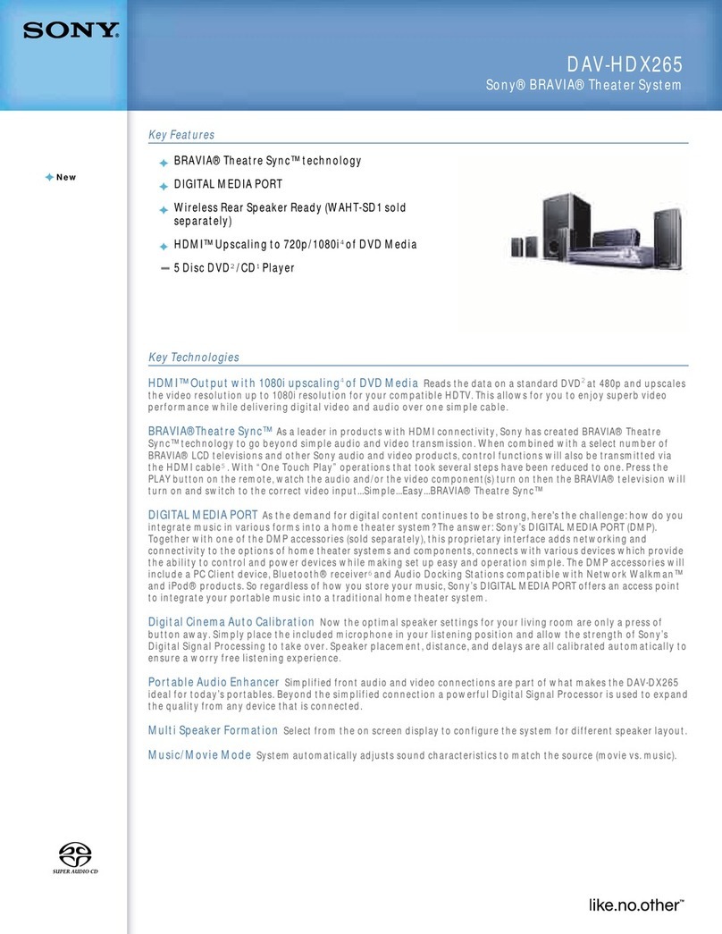
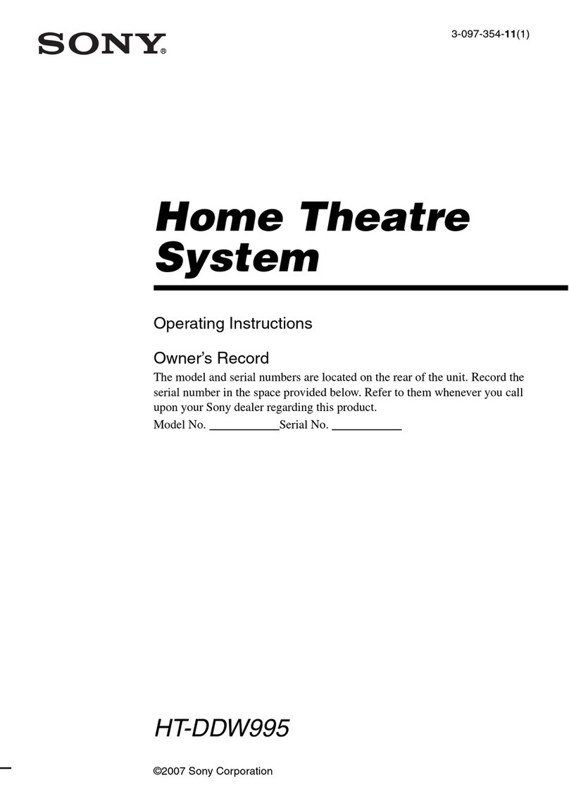
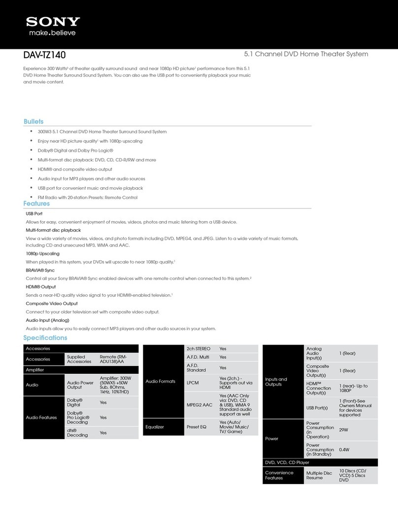
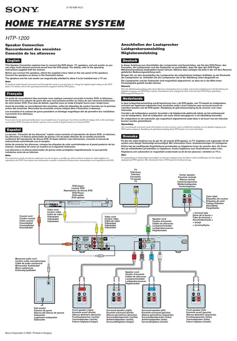
Sony ta-ve170 User manual

TA-VE170
AEP Model
UK Model
E Model
Australian Model
Chinese Model
SERVICE MANUAL
HOME THEATER SYSTEM
Manufactured underlicensefromDolbyLaboratories
Licensing Corporation.
“DOLBY”,“AC-3”,“ProLogic”andthedouble-Dsymbol
;and “Pro Logic” are trademarks of Dolby
Laboratories Licensing Corporation.
• This set is the Amplifier section in
HT-K170.
SPECIFICATIONS
(DIN1 kHz,8 ohms)
25 W + 25 W
(DIN1 kHz,8 ohms)
Front: 25 W /ch
Center: 25 W
Rear: 25 W /ch
TV, VIDEO, DVD2CH,
5.1 CH/DVD:
10 Hz- 50 kHz+0.5/–2 dB
WOOFER:
Voltage: 1 V
Impedance: 1 kilohms
Fullmute
220 - 230 V AC, 50/60Hz
115 W
430 x 274 x 64.5 mm
4.6 kg
Poweroutput
Rated Power
OutputatStereo
mode
Reference
PowerOutput
Frequency
response
Inputs
Outputs
Muting
Power
requirements
Power
consumption
Dimensions
Mass (Approx.)
TV,
VIDEO,
DVD 2CH,
5.1 CH/
DVD
Sensitivity
250 mV
Impedance
50
kilohms
S/N
(weighting
network,
inputlevel)
85
*78IHF
dB*
(A, 250 mV)
General
Design and specifications are subject to
change withoutnotice.
w
w
w
.
x
i
a
o
y
u
1
6
3
.
c
o
m
Q
Q
3
7
6
3
1
5
1
5
0
9
9
2
8
9
4
2
9
8
T
E
L
1
3
9
4
2
2
9
6
5
1
3
9
9
2
8
9
4
2
9
8
0
5
1
5
1
3
6
7
3
Q
Q
TEL 13942296513 QQ 376315150 892498299
http://www.xiaoyu163.com
2
SAFETY-RELATED COMPONENT WARNING!!
COMPONENTS IDENTIFIED BY MARK 0OR DOTTED LINEWITH
MARK 0ON THE SCHEMATIC DIAGRAMS AND INTHE PARTS
LIST ARE CRITICAL TO SAFE OPERATION. REPLACE THESE
COMPONENTS WITH SONY PARTS WHOSE PART NUMBERS
APPEAR AS SHOWN IN THIS MANUAL OR IN SUPPLEMENTS
PUBLISHED BY SONY.
Flexible Circuit Board Repairing
• Keep the temperature of soldering iron around 270˚C
during repairing.
• Do not touch the soldering iron on the same conductor of the
circuit board (within 3 times).
• Be careful not to apply force on the conductor when soldering
or unsoldering.
TABLE OF CONTENTS
1. GENERAL ········································································· 3
2. DISASSEMBLY ································································ 4
3. TEST MODE····································································· 5
4. DIAGRAMS········································································ 6
4-1. Notes for Printed Wiring Board
and Schematic Diagram·················································· 6
4-2. Printed Wiring Board – MAIN Section – ······················ 9
4-3. Schematic Diagram – MAIN Section (1/2) – ·············· 10
4-4. Schematic Diagram – MAIN Section (2/2) – ·············· 11
4-5. Printed Wiring Boards – PANEL Section –················· 12
4-6. Schematic Diagram – PANEL Section – ····················· 13
4-7. Printed Wiring Boards – POWER Section – ··············· 14
4-8. Schematic Diagram – POWER Section –···················· 15
4-9. IC Pin Function Description ········································· 16
5. EXPLODED VIEWS····················································· 17
6. ELECTRICAL PARTS LIST····································· 19
w
w
w
.
x
i
a
o
y
u
1
6
3
.
c
o
m
Q
Q
3
7
6
3
1
5
1
5
0
9
9
2
8
9
4
2
9
8
T
E
L
1
3
9
4
2
2
9
6
5
1
3
9
9
2
8
9
4
2
9
8
0
5
1
5
1
3
6
7
3
Q
Q
TEL 13942296513 QQ 376315150 892498299
http://www.xiaoyu163.com
3
SECTION 1
GENERAL
This section is extracted
from instruction manual.
15.1 CH/DVD
2DVD2CH
3TV
7REAR SPEAKERS
8CENTER SPEAKER
9Mains lead
4VIDEO
5WOOFER
FRONT SPEAKER
6
15 7
9
8642
3
1
3 4 5 6 7 8
2
1?/1 button
2CENTER MODE button
3VIDEO button
4TV button
5DVD 2CH button
65-1 CH/DVD button
7SOUND FIELD button
8MASTER VOLUME knob
w
w
w
.
x
i
a
o
y
u
1
6
3
.
c
o
m
Q
Q
3
7
6
3
1
5
1
5
0
9
9
2
8
9
4
2
9
8
T
E
L
1
3
9
4
2
2
9
6
5
1
3
9
9
2
8
9
4
2
9
8
0
5
1
5
1
3
6
7
3
Q
Q
TEL 13942296513 QQ 376315150 892498299
http://www.xiaoyu163.com
4
CASE, FRONT PANEL SECTION
MAIN BOARD
Note: Follow the disassembly procedure in the numerical order given.
4
case
3
screw (BVTP3 x8)
7
four screws
(BVTP3 x8)
claw
6
flat wire
(CNS301)
2
two tapping screws
1
two tapping screw
s
5
flat wire
(CNS302)
claw
8
front panel section
8
Remove the
MAIN board
to direction of
the arrow
A
6
connector
(CNS800)
5
connector
(CNP802)
7
six screws
(BVTP3 x8)
1
two screws
(BVTP3 x8)
3
six screws
(BVTP3 x8
)
2
DC fan
4
connector
(CNS801)
A
SECTION 2
DISASSEMBLY
w
w
w
.
x
i
a
o
y
u
1
6
3
.
c
o
m
Q
Q
3
7
6
3
1
5
1
5
0
9
9
2
8
9
4
2
9
8
T
E
L
1
3
9
4
2
2
9
6
5
1
3
9
9
2
8
9
4
2
9
8
0
5
1
5
1
3
6
7
3
Q
Q
TEL 13942296513 QQ 376315150 892498299
http://www.xiaoyu163.com

5
SECTION 3
TEST MODE
Thisequipmentisprovidedwithatestmode builtinthemicrocomputer.
The contents are described in the following.
[Initial Mode]
1.
Press ?/1button while pressing both [TV] and
[5.1CH/DVD]
buttons simultaneously.
2. “INITIAL” is displayed on the fluorescent indicator tube, and
the status of the unit is set in the following.
• All Memory is clear.
• Center, rear level set to 0.
• Center mode set to NORMAL.
• Muting clear.
• Volume level set to min.
• FAN is on.
[Factory Mode]
1.
Press
?/1
button while pressing three buttons of
[VIDEO]
,
[DVD2CH]
, and
[5.1CH/DVD]
simultaneously.
2. Factory setting same as initial except center mode set to normal
using jog can set to volume max or min directly.
[FL Check Mode]
1. Press
?/1
button while both
[
CENTERMODE
]
and
[TV]
buttons
simultaneously.
2. Fluorescent indicator tube and LED are checked, “FINISH” is
displayedandthestatusof the unitissetbackin normal condition.
[Gain Up Mode]
1. Press
?/1
button while pressing
[
SOUNDFIELD
]
button.
2. “NOMAL” is displayed on the fluorescent indicator tube and
the rear is gained up 3 dB.
3. To exit from this mode, press two buttons in the same manner as
step1.
“GAIN LOW” is displayed on the fluorescent indicator tube and
the status of the unit is set back in normal condition.
[Version Mode]
1.
Press
?/1
buttonwhilepressingthree buttonsof
[CENTERMODE]
,
[
DVD2CH
]
and
[
SOUNDFIELD
]
buttons simultaneously.
2. Version of its destination is displayed onthefluorescentindicator
tube.
[FAN ON/OFF]
• Press ?/1button while pressing
[CENTERMODE]
button.
• “FAN ON” t fan always turn on.
• “FAN AUTO”t when micro computer detected enough input
signal fan turn on automatically. Normally fan is off.
w
w
w
.
x
i
a
o
y
u
1
6
3
.
c
o
m
Q
Q
3
7
6
3
1
5
1
5
0
9
9
2
8
9
4
2
9
8
T
E
L
1
3
9
4
2
2
9
6
5
1
3
9
9
2
8
9
4
2
9
8
0
5
1
5
1
3
6
7
3
Q
Q
TEL 13942296513 QQ 376315150 892498299
http://www.xiaoyu163.com
6
• Circuit Boards Location
SECTION 4
DIAGRAMS
PW.SW borad
DISPLAY board
JOG board
MAIN boar
d
STANDBY board
PRIMARY board
SECONDARY board
4-1. NOTES FOR PRINTED WIRING BOARD AND SCHEMATIC DIAGRAM
Note on Schematic Diagram:
• All capacitors are in µF unless otherwise noted. pF: µµF
50 WV or less are not indicated except for electrolytics
and tantalums.
• All resistors are in Ωand 1/4W or less unless otherwise
specified.
•¢: internal component.
•2: nonflammable resistor.
•C: panel designation.
Note on PrintedWiring Board:
•X: parts extracted from the component side.
•b: Pattern from the side which enables seeing.
• Indication of transistor.
•U: B+ Line.
•V: B– Line.
• Voltages and waveforms are dc with respect to ground
under no-signal conditions.
• Voltages are takenwithaVOM(Inputimpedance10MΩ).
Voltage variations may be noted due to normal produc-
tion tolerances.
• Waveforms are taken with a oscilloscope.
Voltage variations may be noted due to normal produc-
tion tolerances.
• Circled numbers refer to waveforms.
• Signal path.
F: FRONT/AUDIO IN
f: REAR
E: CENTER
j:WOOFER
C
BThese are omitted.
E
Q
B
These are omitted.
CE
Q
• Waveforms
– MAIN Board –
1IC300 #¡ (OSC)
– DISPLAY Board –
1IC201 #¢ (X1)
3.4 Vp-p
8 MHz
4.3 Vp-p
4.19 MHz
Note:
The components identified
by mark0ordotted linewith
mark0arecriticalforsafety.
Replaceonlywithpart num-
ber specified.
Note:
w
w
w
.
x
i
a
o
y
u
1
6
3
.
c
o
m
Q
Q
3
7
6
3
1
5
1
5
0
9
9
2
8
9
4
2
9
8
T
E
L
1
3
9
4
2
2
9
6
5
1
3
9
9
2
8
9
4
2
9
8
0
5
1
5
1
3
6
7
3
Q
Q
TEL 13942296513 QQ 376315150 892498299
http://www.xiaoyu163.com
7
• IC Block Diagrams
– STANDBY Board –
IC950 NJM2103D
IC500 LC78212
– MAIN Board –
IC100 M62447SP
1
2
3
45
6
7
8
V+
VSB/SESIN
VSA
RESET
GND
OUTC
VSC
CR
VREF
+–
–+
–
+
–
+
Q
R S
2
1
4
3
6
5
8
7
10
9
12
11
14
13
16
15
18
17
41
42
39
40
37
38
35
36
33
34
31
32
29
30
OUTPUT
PORT
MICRO
COMPUTER
INTERFACE
DVDD
CLK
DATA
LATCH
DGND
AGND
OUT4
OUT3
OUT2
OUT1
AVDD
SW IN
GND S
SR IN
SL IN
GND C
C IN
GND R1
GND R2
GND L1
GND L2
R IN
GND LR
L IN
SW OUT
SR OUT
SL OUT
C OUT
R OUT
NC
L OUT
AVSS1
AVSS2
22 – 28
NC
21 – 19
1
2
3
4
5
6
7
8
9
10
11
12
13
14
15
30
29
28
27
26
25
24
23
22
21
20
19
18
17
16
CONTROL
LATCH
SHIFT RESISTOR
LEVEL SHIFT
CL
DI
CE
VEE
OUT
IN
OUT
IN
OUT
IN
VSS
S
RESET
VDD
OUT
IN
IN
OUT
IN
OUT
IN
w
w
w
.
x
i
a
o
y
u
1
6
3
.
c
o
m
Q
Q
3
7
6
3
1
5
1
5
0
9
9
2
8
9
4
2
9
8
T
E
L
1
3
9
4
2
2
9
6
5
1
3
9
9
2
8
9
4
2
9
8
0
5
1
5
1
3
6
7
3
Q
Q
TEL 13942296513 QQ 376315150 892498299
http://www.xiaoyu163.com
8
IC300 LV1035M
STRIM
OSC
VOL
VOL
VCA VCA A
B
A
B
VCA VCA
VCA VCA VCA VCA
DEV
NOISE
GEN
NOISE
FILTER
BPF
CONTROL
CH
CONTROL
BPF
V REF
STRIM
S
MODE
RECT
RECT
DC
CUT
B NR
OUT
FILTER
DATA
DECODER
VOL/
MUTE
BPF
RECT
LOGIC
FF
LOGIC
FF RECT
C MODE
LOGIC LOGIC
S
S
S
AAS
B
BB
A
B
C
B
LR
AA
A
B
A
B
A
B
A
B
A
B
S
VDD
PCM
PCM
CONTROL
SRAM
IN
FILTER
R
L
C
S
R
A
B
A
B
A
B
A
B
L
L
R
L
R
R BPF2
R BPF1
S DC OUT
C DC OUT
R DC OUT
L DC OUT
V REF
VCC
C OUT
S OUT
R OUT
L OUT
GND
L IN
R IN
S IN
DELAY OUT
L BPF2
L BPF1
RT IN
LT IN
DC CUT
C MODE
GND
NS BPF1
OSC
NS BPF2
ENABLE
DATA
CLK
DATA
CLK
VSS
OSC
OSC
VDD
A/D
NS
D/A
DC CUT
DC CUT
VCC
DET
IREF
GND
S-OUT
R-OUT
L-OUT
L RECT
DC CUT4
R RECT
DC CUT3
L BPF3
VLR TH
VLR 1
VLR 2
VCS 2
VCS 1
VCS TH
L+R RECT
DC CUT2
L-R RECT
DC CUT1
R BPF3
64 63 62 61 60 59 58 57 56 55 54 53 52 51 50 49
48
47
46
45
44
43
41
40
39
38
37
36
35
34
33
1817
16
15
14
13
12
11
10
9
7
3
4
5
6
1
2
8
19 20 21 22 23 24 25 26 27 28 29 30 31 32
42
w
w
w
.
x
i
a
o
y
u
1
6
3
.
c
o
m
Q
Q
3
7
6
3
1
5
1
5
0
9
9
2
8
9
4
2
9
8
T
E
L
1
3
9
4
2
2
9
6
5
1
3
9
9
2
8
9
4
2
9
8
0
5
1
5
1
3
6
7
3
Q
Q
TEL 13942296513 QQ 376315150 892498299
http://www.xiaoyu163.com

TA-VE170
99
D100 J-13
D310 C-6
D520 C-12
D521 J-13
D550 I-8
D620 C-11
D621 J-13
D720 C-8
D721 J-7
D731 J-6
D801 G-12
D810 H-12
D811 H-12
D812 H-11
D813 H-11
D814 D-4
D820 I-12
D821 I-12
D822 I-12
D823 I-12
D850 C-13
D853 C-13
IC100 I-2
IC300 E-3
IC302 E-6
IC401 C-4
IC500 G-3
IC501 I-10
IC502 F-6
IC503 F-5
IC601 F-10
IC651 D-10
IC701 E-9
IC751 H-9
IC801 I-6
IC802 I-7
IC803 E-5
Q150 I-5
Q151 I-5
Q152 I-4
Q153 I-4
Q154 I-4
Q155 I-4
Q367 C-6
Q520 D-12
Q550 I-8
Q551 I-9
Q620 D-12
Q720 C-8
Q730 I-7
Q731 I-6
Q732 J-7
Q851 C-13
Q853 B-13
Q854 C-12
Q855 B-13
4-2. PRINTED WIRING BOARD – MAIN Section –
• Semiconductor
Location
Ref. No. Location
• See page 6 for Circuit Boards Location. There are a few cases that the part printed on
this diagram isn’t mounted in this model.
(Page 12)(Page 12) (Page 12)
(Page 14)
(Page 14)
(FAN1)
w
w
w
.
x
i
a
o
y
u
1
6
3
.
c
o
m
Q
Q
3
7
6
3
1
5
1
5
0
9
9
2
8
9
4
2
9
8
T
E
L
1
3
9
4
2
2
9
6
5
1
3
9
9
2
8
9
4
2
9
8
0
5
1
5
1
3
6
7
3
Q
Q
TEL 13942296513 QQ 376315150 892498299
http://www.xiaoyu163.com
TA-VE170
1010
4-3. SCHEMATIC DIAGRAM – MAIN Section (1/2) – • See page 6 for Waveform. • See page 7 for IC Block Diagrams.
R106 100k
2
w
w
w
.
x
i
a
o
y
u
1
6
3
.
c
o
m
Q
Q
3
7
6
3
1
5
1
5
0
9
9
2
8
9
4
2
9
8
T
E
L
1
3
9
4
2
2
9
6
5
1
3
9
9
2
8
9
4
2
9
8
0
5
1
5
1
3
6
7
3
Q
Q
TEL 13942296513 QQ 376315150 892498299
http://www.xiaoyu163.com
TA-VE170
1212
4-5. PRINTED WIRING BOARDS – PANEL Section –
• Semiconductor
Location
Ref. No. Location
• See page 6 for Circuit Boards Location. There are a few cases that the part printed on
this diagram isn’t mounted in this model.
(Page 9)
(Page 9)
.
D201 B-11
D202 B-11
D203 C-3
D204 C-3
D211 B-11
D212 B-11
D213 B-11
D214 B-11
D215 B-5
D216 B-5
D217 B-5
D218 B-4
IC201 C-8
IC202 B-10
Q201 C-3
Q202 C-3
Q218 B-2
w
w
w
.
x
i
a
o
y
u
1
6
3
.
c
o
m
Q
Q
3
7
6
3
1
5
1
5
0
9
9
2
8
9
4
2
9
8
T
E
L
1
3
9
4
2
2
9
6
5
1
3
9
9
2
8
9
4
2
9
8
0
5
1
5
1
3
6
7
3
Q
Q
TEL 13942296513 QQ 376315150 892498299
http://www.xiaoyu163.com
TA-VE170
1313
4-6. SCHEMATIC DIAGRAM – PANEL Section – • See page 6 for Waveform. • See page 16 for IC Pin Function.
(Page 10)
(Page 11)
PIN FUNCTION
w
w
w
.
x
i
a
o
y
u
1
6
3
.
c
o
m
Q
Q
3
7
6
3
1
5
1
5
0
9
9
2
8
9
4
2
9
8
T
E
L
1
3
9
4
2
2
9
6
5
1
3
9
9
2
8
9
4
2
9
8
0
5
1
5
1
3
6
7
3
Q
Q
TEL 13942296513 QQ 376315150 892498299
http://www.xiaoyu163.com

TA-VE170
1414
4-7. PRINTED WIRING BOARDS – POWER Section – • See page 6 for Circuit Boards Location. There are a few cases that the part printed on
this diagram isn’t mounted in this model.
(Page 9)
(Page 9)
PC900
w
w
w
.
x
i
a
o
y
u
1
6
3
.
c
o
m
Q
Q
3
7
6
3
1
5
1
5
0
9
9
2
8
9
4
2
9
8
T
E
L
1
3
9
4
2
2
9
6
5
1
3
9
9
2
8
9
4
2
9
8
0
5
1
5
1
3
6
7
3
Q
Q
TEL 13942296513 QQ 376315150 892498299
http://www.xiaoyu163.com
1616
4-9. IC PIN FUNCTION DESCRIPTION
•DISPLAY BOARD IC201 µPD78042FGF-120-3B9 (SYSTEM CONTROLLER, FL/LED DRIVER, KEY CONTROL)
Pin No. Pin Name I/O Function
1 to 7 DIG7 to DIG1 O Grid drive signal output to the fluorescent indicator tube (FL201)
8 VDD — Power supply terminal (+5V)
9 S. CLK O Serial data transfer clock signal output to the M62447SP (IC100), LV1035M (IC300) and
LC78212 (IC500)
10 S. DATA O Serial data output to the M62447SP (IC100), LV1035M (IC300) and LC78212 (IC500)
11 S. CE (VOL) O Chip enable signal output to the M62447SP (IC100) “H” active
12 S. CE (LC7822) O Chip enable signal output to the LC78212 (IC500) “H” active
13
S. CE (LV1035M)
OChip enable signal output to the LV1035M (IC300) “H” active
14 EN3 O Enable signal output terminal “L” active
15 — Not used
16 PROTECT I
I
Overload protection input terminal
17 RESET I System reset signal input from the reset signal generator circuit “L”: reset
For several hundreds msec. after the power supply rises, “L” is input, then it changes to “H”
18 EN1 O Enable signal output to the function switch (IC402) “L” active
19 EN2 O Enable signal output to the function switch (IC401) “L” active
20 AVSS — Ground terminal (for A/D converter)
21 FAN CLK I Fan motor clock signal input terminal
22 FAN ON I Fan on signal input for the fan motor drive
23 FAN. CNTL O Fan motor control signal output terminal “L”: fan motor on (high speed) “H” : fan low speed
24 MUTING O LED drive signal output of the MUTING LED (D218) “H”: LED on
25 — I Not used (open)
26 A/D III I Key input terminal (A/D input) S205, 206 (5.1 IN, SURROUND MODE keys input)
27 A/D II I Key input terminal (A/D input) S202, 204 (VIDEO, DVD keys input)
28 A/D I I Key input terminal (A/D input) S201, 203 (CENTER MODE, TV keys input)
29 AVDD — Power supply terminal (+5V) (for A/D converter)
30 AVREF I Reference voltage (+5V) input terminal (for A/D converter)
31 XT1 I Sub system clock input terminal Not used (fixed at “L”)
32 XT2 O Sub system clock output terminal Not used (open)
33 VSS — Ground terminal
34 X1 I Main system clock input terminal (4.19 MHz)
35 X2 O Main system clock output terminal (4.19 MHz)
36 SIMULATED O LED drive signal output of the SIMULATED LED (D215) “L”: LED on
37 C. STUDIO O LED drive signal output of the C.STUDIO LED (D216) “L”: LED on
38 PROLOGIC O LED drive signal output of the PROLOGIC LED (D217) “L”: LED on
39 — I Not used (fixed at “L”)
40 PHANTOM O LED drive signal output of the PHANTOM LED (D211) “L”: LED on
41 WIDE O LED drive signal output of the WIDE LED (D212) “L”: LED on
42 NORMAL O LED drive signal output of the NORMAL LED (D213) “L”: LED on
43 3-STEREO O LED drive signal output of the 3 STEREO LED (D214) “L”: LED on
44 SYS. POWER I System power on/off switch (S200 I/u) input terminal
45 ENCODER 2 I Jog dial pulse input from the rotary encoder (RV201 MASTER VOLUME)
46 ENCODER 1 I Jog dial pulse input from the rotary encoder (RV201 MASTER VOLUME)
47 STOP I Power down detection signal input from the NJM2103D (IC950) “L”: power down
48 VSS — Ground terminal
49 SIRCS I Sircs signal input from the remote control receiver (IC202)
50, 51 — I Not used (fixed at “L”)
Pin No. Pin Name I/O Function
52 VDD — Power supply terminal (+5V)
53 FAN ON/OFF OFan on/off control “L” : fan on “H” : fan stop
54 MUTE. S. R O Line muting on/off control signal output for the rear speaker right channel signal
“H”: muting on
55 MUTE. S. L O Line muting on/off control signal output for the rear speaker left channel signal
“H”: muting on
56 FUNC. MUTE O Line muting on/off control signal output for the front and center speakers signal
“H”: muting on
57 VERSION I Setting terminal for the version (fixed at “L” in this set)
58 W. RY O Woofer on/off relay drive signal output terminal “H”: relay on
59 SP. RY O Front speaker on/off relay drive signal output terminal (for protect) “H”: relay on
60 S. RY O Rear speaker on/off relay drive signal output terminal (for protect) “H”: relay on
61 C. RY O Center speaker on/off relay drive signal output terminal (for protect) “H”: relay on
62 POWER. RY O Power on/off relay drive signal output terminal “H”: relay on (power on)
63 to 70 S14 to S7 O Segment drive signal output to the fluorescent indicator tube (FL201)
71 VLOAD — Power supply terminal (–24V) (for FL drive)
72 to 77 S6 to S1 O Segment drive signal output to the fluorescent indicator tube (FL201)
78 — O Not used (open)
79, 80 DIG9, DIG8 O Grid drive signal output to the fluorescent indicator tube (FL201)
w
w
w
.
x
i
a
o
y
u
1
6
3
.
c
o
m
Q
Q
3
7
6
3
1
5
1
5
0
9
9
2
8
9
4
2
9
8
T
E
L
1
3
9
4
2
2
9
6
5
1
3
9
9
2
8
9
4
2
9
8
0
5
1
5
1
3
6
7
3
Q
Q
TEL 13942296513 QQ 376315150 892498299
http://www.xiaoyu163.com
17
SECTION 5
EXPLODED VIEWS
• Items marked “*” are not stocked since they
are seldom required for routine service. Some
delay should be anticipated when ordering these
items.
• The mechanical parts with no reference num-
ber in the exploded views are not supplied.
• Accessories and packing materials are given in
the last of the electrical parts list.
NOTE:
• -XX and -X mean standardized parts, so they
may have some difference from the original
one.
• Color Indication of Appearance Parts
Example:
KNOB, BALANCE (WHITE) . . . (RED)
↑↑
Parts Color Cabinet's Color
The components identified by mark 0or
dotted line with mark 0are critical for safety.
Replace only with part number specified.
(1) CASE, FRONT PANEL SECTION
Ref. No. Part No. Description Remark Ref. No. Part No. Description Remark
6
5
5
78
5
11
9
12
10
9
12
2
1
supplied
with RV201
CHASSIS SECTION
4
3
1 4-211-178-01 KNOB (VOL) (BLACK)
1 4-211-178-21 KNOB (VOL) (SILVER)
2 X-4953-052-1 FRONT PANEL ASSY (BLACK)
2 X-4953-053-1 FRONT PANEL ASSY (SILVER)
3 3-008-600-11 EMBLEM (5-AR), SONY
4 1-678-814-11 PW.SW BOARD
5 4-951-620-01 SCREW(2.6X8), +BVTP
6 1-777-353-11 WIRE(FLAT TYPE) (15 CORE)
7 A-4473-758-A DISPLAY BOARD,COMPLETE
8 1-769-973-11 WIRE(FLAT TYPE) (13 CORE)
9 3-710-901-11 SCREW, TAPPING (BLACK)
9 4-210-291-11 SCREW (CASE 3 TP2)(SILVER)
10 4-211-182-51 CASE (SILVER)
*10 4-211-182-01 CASE (BLACK)
11 1-678-808-11 JOG BOARD
12 7-685-646-79 SCREW +BVTP3X8 TYPE2 N-S
w
w
w
.
x
i
a
o
y
u
1
6
3
.
c
o
m
Q
Q
3
7
6
3
1
5
1
5
0
9
9
2
8
9
4
2
9
8
T
E
L
1
3
9
4
2
2
9
6
5
1
3
9
9
2
8
9
4
2
9
8
0
5
1
5
1
3
6
7
3
Q
Q
TEL 13942296513 QQ 376315150 892498299
http://www.xiaoyu163.com
18
(2) CHASSIS SECTION
Ref. No. Part No. Description Remark Ref. No. Part No. Description Remark
60
59
61
58
58
58
62
51
52
56
55
54
54
53
53
T900
FAN1
PC900
63
57
58
58
*51 4-211-183-21 CHASSIS PANEL
52 1-678-812-11 SECONDARY BOARD
53 4-212-070-01 INSULATOR (PT)
54 3-531-576-11 RIVET
55 7-685-880-09 SCREW +BVTT4X6 (S)
56 1-678-811-11 PRIMARY BOARD
57 A-4473-760-A STANDBY BOARD,COMPLETE
58 7-685-646-79 SCREW +BVTP3X8 TYPE2 N-S
59 A-4473-763-A MAIN BOARD,COMPLETE
*60 4-924-098-21 HOLDER, PC BOARD
*61 3-703-244-00 BUSHING (2104), CORD
62 4-965-822-01 FOOT
63 4-214-557-11 CUSHION
FAN1 1-763-137-11 FAN, DC
0T900 1-431-979-11 TRANSFORMER, POWER
0PC900 1-777-071-21 CORD, POWER
The components identified by
mark 0or dotted line with mark
0are critical for safety.
Replace only with part number
specified.
w
w
w
.
x
i
a
o
y
u
1
6
3
.
c
o
m
Q
Q
3
7
6
3
1
5
1
5
0
9
9
2
8
9
4
2
9
8
T
E
L
1
3
9
4
2
2
9
6
5
1
3
9
9
2
8
9
4
2
9
8
0
5
1
5
1
3
6
7
3
Q
Q
TEL 13942296513 QQ 376315150 892498299
http://www.xiaoyu163.com
19
SECTION 6
ELECTRICAL PARTS LIST
NOTE:
• Due to standardization, replacements in the
parts list may be different from the parts
specified in the diagrams or the components
used on the set.
• -XX and -X mean standardized parts, so
they may have some difference from the
original one.
• RESISTORS
All resistors are in ohms.
METAL: Metal-film resistor.
METAL OXIDE: Metal oxide-film resistor.
F: nonflammable
• Items marked “*” are not stocked since they
are seldom required for routine service.
Some delay should be anticipated when order-
ing these items.
• SEMICONDUCTORS
In each case, u: µ, for example:
uA. . : µA. . uPA. . : µPA. .
uPB. . : µPB. . uPC. . : µPC. .
uPD. . : µPD. .
• CAPACITORS
uF: µF
• COILS
uH: µH
The components identified by mark 0or
dotted line with mark 0are critical for safety.
Replace only with part number specified.
When indicating parts by reference number,
please include the board name.
Ref. No. Part No. Description Remark Ref. No. Part No. Description Remark
A-4473-758-A DISPLAY BOARD, COMPLETE
***********************
*4-921-941-01 CUSHION (FL)
*4-943-107-11 HOLDER (FL TUBE)
< CAPACITOR >
C201 1-104-905-11 CAPACITOR 0.22F 5.5V
C202 1-164-159-11 CERAMIC 0.1uF 50V
C203 1-162-294-31 CERAMIC 0.001uF 10% 50V
C204 1-124-261-00 ELECT 10uF 20% 50V
C205 1-124-465-00 ELECT 0.47uF 20% 50V
C206 1-164-159-11 CERAMIC 0.1uF 50V
C207 1-162-282-31 CERAMIC 100PF 10% 50V
C208 1-162-282-31 CERAMIC 100PF 10% 50V
C210 1-164-159-11 CERAMIC 0.1uF 50V
C211 1-164-159-11 CERAMIC 0.1uF 50V
C212 1-164-159-11 CERAMIC 0.1uF 50V
< CONNECTOR >
*CNP203 1-565-295-11 PLUG, CONNECTOR 4P
*CNS201 1-569-306-11 SOCKET, CONNECTOR (L TYPE) 15P
CNS202 1-568-444-11 SOCKET, CONNECTOR 13P
*CNS203 1-565-480-11 CONNECTOR, BOARD TO BOARD 4P
CNS802 1-770-480-11 SOCKET, CONNECTOR PIN 4P
< DIODE >
D201 8-719-911-19 DIODE 1SS133T-72
D202 8-719-911-19 DIODE 1SS133T-72
D203 8-719-911-19 DIODE 1SS133T-72
D204 8-719-911-19 DIODE 1SS133T-72
D211 8-719-046-36 DIODE SEL5921A-TP15 (PHANTOM)
D212 8-719-046-36 DIODE SEL5921A-TP15 (WIDE)
D213 8-719-046-36 DIODE SEL5921A-TP15 (NORMAL)
D214 8-719-046-36 DIODE SEL5921A-TP15 (3 STEREO)
D215 8-719-046-36 DIODE SEL5921A-TP15 (SIMULATED)
D216 8-719-046-36 DIODE SEL5921A-TP15 (C. STUDIO)
D217 8-719-046-36 DIODE SEL5921A-TP15 (PRO LOGIC)
D218 8-719-046-36 DIODE SEL5921A-TP15 (MUTING)
< FILTER >
FL201 1-517-786-11 INDICATOR TUBE, FLUORESCENT
< IC >
IC201 8-759-683-98 IC uPD78042FGF-120-3B9
IC202 8-759-332-18 IC GP1U27XB
< COIL >
L201 1-410-509-11 INDUCTOR 10uH
< TRANSISTOR >
Q201 8-729-900-63 TRANSISTOR BN1F4M-TP
Q202 8-729-900-36 TRANSISTOR BA1F4M-TP
Q218 8-729-119-76 TRANSISTOR 2SA1115TP-F
< RESISTOR >
R200 1-249-433-11 CARBON 22K 5% 1/4W
R201 1-247-903-00 CARBON 1M 5% 1/4W
R203 1-249-441-11 CARBON 100K 5% 1/4W
R204 1-249-425-11 CARBON 4.7K 5% 1/4W F
R205 1-249-437-11 CARBON 47K 5% 1/4W
R206 1-249-429-11 CARBON 10K 5% 1/4W
R207 1-249-429-11 CARBON 10K 5% 1/4W
R208 1-249-429-11 CARBON 10K 5% 1/4W
R209 1-249-433-11 CARBON 22K 5% 1/4W
R210 1-247-807-31 CARBON 100 5% 1/4W
R211 1-247-807-31 CARBON 100 5% 1/4W
R215 1-247-807-31 CARBON 100 5% 1/4W
R219 1-249-409-11 CARBON 220 5% 1/4W F
R221 1-247-807-31 CARBON 100 5% 1/4W
R222 1-247-807-31 CARBON 100 5% 1/4W
R223 1-247-807-31 CARBON 100 5% 1/4W
R224 1-247-807-31 CARBON 100 5% 1/4W
R225 1-247-807-31 CARBON 100 5% 1/4W
R226 1-247-807-31 CARBON 100 5% 1/4W
R227 1-249-433-11 CARBON 22K 5% 1/4W
R228 1-249-433-11 CARBON 22K 5% 1/4W
R229 1-249-425-11 CARBON 4.7K 5% 1/4W F
R230 1-249-429-11 CARBON 10K 5% 1/4W
R231 1-249-425-11 CARBON 4.7K 5% 1/4W F
R232 1-249-425-11 CARBON 4.7K 5% 1/4W F
R233 1-249-425-11 CARBON 4.7K 5% 1/4W F
R234 1-249-425-11 CARBON 4.7K 5% 1/4W F
R235 1-249-425-11 CARBON 4.7K 5% 1/4W F
R236 1-249-425-11 CARBON 4.7K 5% 1/4W F
R238 1-249-441-11 CARBON 100K 5% 1/4W
< SWITCH >
S201 1-762-875-21 SWITCH, KEYBOARD (CENTER MODE)
S202 1-762-875-21 SWITCH, KEYBOARD (DVD 2CH)
S203 1-762-875-21 SWITCH, KEYBOARD (VIDEO)
S204 1-762-875-21 SWITCH, KEYBOARD (TV)
S205 1-762-875-21 SWITCH, KEYBOARD (5.1CH/DVD)
DISPLAY
w
w
w
.
x
i
a
o
y
u
1
6
3
.
c
o
m
Q
Q
3
7
6
3
1
5
1
5
0
9
9
2
8
9
4
2
9
8
T
E
L
1
3
9
4
2
2
9
6
5
1
3
9
9
2
8
9
4
2
9
8
0
5
1
5
1
3
6
7
3
Q
Q
TEL 13942296513 QQ 376315150 892498299
http://www.xiaoyu163.com
Ref. No. Part No. Description Remarks Ref. No. Part No. Description Remarks
20
S206 1-762-875-21 SWITCH, KEYBOARD (SOUND FIELD)
< VIBRATOR >
X201 1-577-101-11 VIBRATOR, CERAMIC (4.19MHz)
************************************************************
1-678-808-11 JOG BOARD
*********
< VARIABLE RESISTOR >
RV201 1-475-886-11 ENCODER, ROTARY (MASTER VOLUME)
************************************************************
A-4473-763-A MAIN BOARD, COMPLETE
*********************
3-531-576-11 RIVET
7-685-647-79 SCREW +BVTP 3X10 TYPE2 N-S
7-685-872-09 SCREW +BVTT 3X8 (S)
< CAPACITOR >
C101 1-126-163-11 ELECT 4.7uF 20% 50V
C102 1-126-163-11 ELECT 4.7uF 20% 50V
C103 1-126-163-11 ELECT 4.7uF 20% 50V
C104 1-126-163-11 ELECT 4.7uF 20% 50V
C105 1-126-163-11 ELECT 4.7uF 20% 50V
C106 1-126-163-11 ELECT 4.7uF 20% 50V
C107 1-162-291-31 CERAMIC 560PF 10.00% 50V
C108 1-126-163-11 ELECT 4.7uF 20% 50V
C109 1-126-163-11 ELECT 4.7uF 20% 50V
C110 1-126-163-11 ELECT 4.7uF 20% 50V
C111 1-126-163-11 ELECT 4.7uF 20% 50V
C112 1-126-163-11 ELECT 4.7uF 20% 50V
C113 1-126-163-11 ELECT 4.7uF 20% 50V
C114 1-164-159-11 CERAMIC 0.1uF 50V
C115 1-126-964-11 ELECT 10uF 20.00% 50V
C116 1-126-964-11 ELECT 10uF 20.00% 50V
C117 1-164-159-11 CERAMIC 0.1uF 50V
C118 1-164-159-11 CERAMIC 0.1uF 50V
C119 1-126-964-11 ELECT 10uF 20.00% 50V
C150 1-164-159-11 CERAMIC 0.1uF 50V
C151 1-164-159-11 CERAMIC 0.1uF 50V
C152 1-164-159-11 CERAMIC 0.1uF 50V
C153 1-164-159-11 CERAMIC 0.1uF 50V
C154 1-164-159-11 CERAMIC 0.1uF 50V
C155 1-164-159-11 CERAMIC 0.1uF 50V
C302 1-126-934-11 ELECT 220uF 20.00% 10V
C303 1-130-494-11 MYLAR 0.082uF 5% 50V
C304 1-137-367-11 MYLAR 0.0033uF 5.00% 50V
C305 1-130-494-11 MYLAR 0.082uF 5% 50V
C306 1-126-959-11 ELECT 0.47uF 20.00% 50V
C307 1-126-964-11 ELECT 10uF 20.00% 50V
C308 1-126-964-11 ELECT 10uF 20.00% 50V
C309 1-162-291-31 CERAMIC 560PF 10.00% 50V
C310 1-126-962-11 ELECT 3.3uF 20.00% 50V
C311 1-126-961-11 ELECT 2.2uF 20.00% 50V
C312 1-126-934-11 ELECT 220uF 20.00% 10V
C313 1-126-934-11 ELECT 220uF 20.00% 10V
C314 1-136-165-00 MYLAR 0.1uF 5.00% 50V
C315 1-164-159-11 CERAMIC 0.1uF 50V
C316 1-124-252-00 ELECT 0.33uF 20% 50V
C317 1-164-159-11 CERAMIC 0.1uF 50V
C318 1-136-357-11 MYLAR 680PF 5.00% 50V
C322 1-126-962-11 ELECT 3.3uF 20.00% 50V
C323 1-136-173-00 MYLAR 0.47uF 5.00% 50V
C324 1-104-664-11 ELECT 47uF 20.00% 16V
C325 1-136-165-00 MYLAR 0.1uF 5.00% 50V
C326 1-136-165-00 MYLAR 0.1uF 5.00% 50V
C327 1-126-959-11 ELECT 0.47uF 20.00% 50V
C328 1-126-163-11 ELECT 4.7uF 20% 50V
C329 1-126-959-11 ELECT 0.47uF 20.00% 50V
C330 1-126-163-11 ELECT 4.7uF 20% 50V
C331 1-124-250-11 ELECT 0.15uF 20.00% 50V
C332 1-126-962-11 ELECT 3.3uF 20.00% 50V
C333 1-124-250-11 ELECT 0.15uF 20.00% 50V
C334 1-137-372-11 MYLAR 0.022uF 5.00% 50V
C335 1-136-161-00 MYLAR 0.047uF 5.00% 50V
C336 1-126-934-11 ELECT 220uF 20.00% 10V
C337 1-126-964-11 ELECT 10uF 20.00% 50V
C338 1-126-964-11 ELECT 10uF 20.00% 50V
C339 1-126-964-11 ELECT 10uF 20.00% 50V
C340 1-126-964-11 ELECT 10uF 20.00% 50V
C341 1-126-934-11 ELECT 220uF 20.00% 10V
C342 1-126-962-11 ELECT 3.3uF 20.00% 50V
C343 1-126-962-11 ELECT 3.3uF 20.00% 50V
C344 1-136-165-00 MYLAR 0.1uF 5.00% 50V
C345 1-136-165-00 MYLAR 0.1uF 5.00% 50V
C346 1-126-959-11 ELECT 0.47uF 20.00% 50V
C347 1-126-163-11 ELECT 4.7uF 20% 50V
C348 1-126-959-11 ELECT 0.47uF 20.00% 50V
C349 1-126-163-11 ELECT 4.7uF 20% 50V
C350 1-124-250-11 ELECT 0.15uF 20.00% 50V
C351 1-126-962-11 ELECT 3.3uF 20.00% 50V
C352 1-124-250-11 ELECT 0.15uF 20.00% 50V
C357 1-164-159-11 CERAMIC 0.1uF 50V
C359 1-126-163-11 ELECT 4.7uF 20% 50V
C360 1-126-163-11 ELECT 4.7uF 20% 50V
C361 1-164-159-11 CERAMIC 0.1uF 50V
C362 1-162-294-31 CERAMIC 0.001uF 10% 50V
C370 1-164-159-11 CERAMIC 0.1uF 50V
C371 1-126-966-11 ELECT 33uF 20.00% 16V
C401 1-164-159-11 CERAMIC 0.1uF 50V
C402 1-164-159-11 CERAMIC 0.1uF 50V
C501 1-126-163-11 ELECT 4.7uF 20% 50V
C502 1-162-282-31 CERAMIC 100PF 10% 50V
C503 1-162-282-31 CERAMIC 100PF 10% 50V
C504 1-102-942-00 CERAMIC 5.0PF 50V
C506 1-104-665-11 ELECT 100uF 20.00% 16V
C507 1-126-160-11 ELECT 1uF 20% 50V
C509 1-137-372-11 MYLAR 0.022uF 5.00% 50V
C511 1-126-163-11 ELECT 4.7uF 20% 50V
DISPLAY JOG MAIN
w
w
w
.
x
i
a
o
y
u
1
6
3
.
c
o
m
Q
Q
3
7
6
3
1
5
1
5
0
9
9
2
8
9
4
2
9
8
T
E
L
1
3
9
4
2
2
9
6
5
1
3
9
9
2
8
9
4
2
9
8
0
5
1
5
1
3
6
7
3
Q
Q
TEL 13942296513 QQ 376315150 892498299
http://www.xiaoyu163.com
Table of contents
Other Sony Home Theater System manuals
Sony
Sony DAV-DZ830W User manual

Sony
Sony HT-7000DH User manual

Sony
Sony DAV-TZ140 User manual

Sony
Sony 4-130-029-13(1) User manual

Sony
Sony DAV-FC7 - Dvd Dream System User manual

Sony
Sony DAV-BC250 - Dvd Home Theater System User manual

Sony
Sony BDV-E500W Mounting instructions

Sony
Sony HT-XT1 User guide

Sony
Sony DAV-C900 - Compact Av System User manual

Sony
Sony BDV-F700 User manual

Sony
Sony HT-K250 User manual

Sony
Sony DAV-DZ250M User manual

Sony
Sony HT-5500D Instruction manual

Sony
Sony HT-SS360 User manual

Sony
Sony HT-CT260 User manual

Sony
Sony DAV-TZ215 User manual

Sony
Sony Esprit TAV-L1 User manual

Sony
Sony SA-VE145 User manual

Sony
Sony 3-283-028-11(1) User manual

Sony
Sony DAV-TZ215 User manual