7
NW-S4
Work procedure
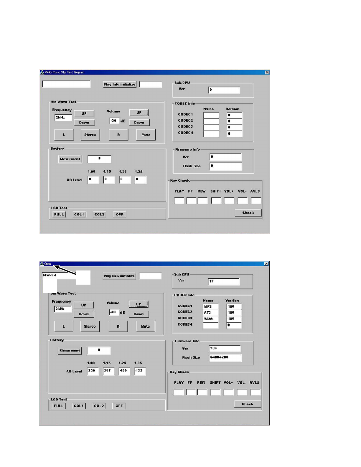
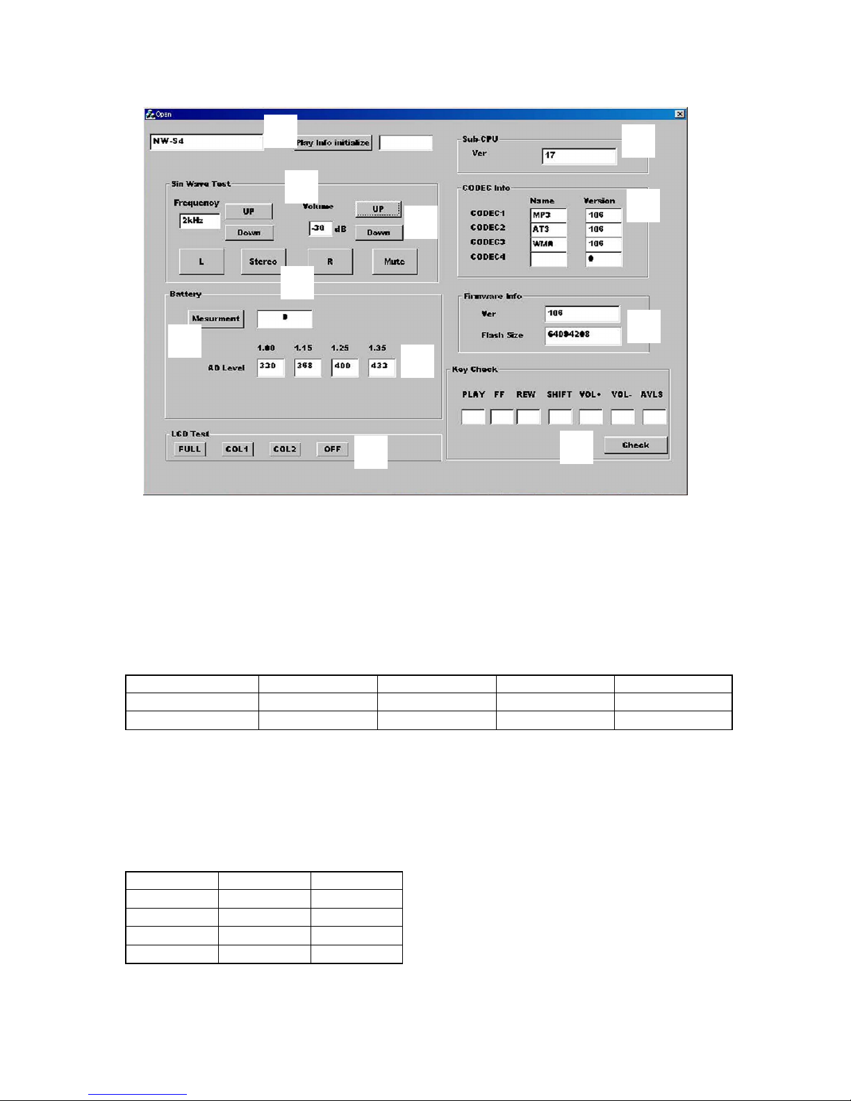
1. Execution of Play Info Initialize
If the MAIN board was replaced for repair, execute “Play Info Initialize”in block qd to return respective functions to initial positions (see
Table 1-5).
Note: In executing the “Play Info Initialize”, set the slide switches to the following positions.
AVLS switch ..... NORM
HOLD switch .... OFF
Table 1-5.
Function Position
Play position Head of first music
VOL level 25
MEGA BASS OFF
PLAY MODE OFF
2. Check after Work
(1) After work, check that the set operates normally through the operation in 1-3. “Operation Check for Inspection (Test Mode)”(see page
3).
(2) Make sure that the check-out and check-in can be made using the PC applications “OpenMG Jukebox”(CODEC programs “MP3”and
“ATRAC3”) and “Windows Media Player 7”(CODEC program “WMA”). Also, make sure that the checked out data can be played
normally.
Note: Do not start up the “OpenMG Jukebox”and the “Windows Media Player 7”simultaneously.
(3) For an installation and acquisition method of “Windows Media Player 7”(CODEC program “WMA”), refer to the following instruction.
16
Using Network Walkman in
combination with Windows
Media
TM
Player 7
If you install Microsoft Win ows Me ia
TM
Player 7,
you can transfer a WMA file to your Network
Walkman an play it back. Refer to the online help for
Win ows Me ia Player 7 for etaile operations.
Playing back WMA files with Network
Walkman
Installing Windows Media Player 7 and the
dedicated plug-ins
• Refer to http://www.openmg.com/ for the etails
on how to obtain Win ows Me ia Player 7.
• To use Win ows Me ia Player 7 in combination
with your Network Walkman, you nee to install
the e icate plug-in software. This software has
been alrea y installe when the NW-S4 river was
installe using the enclose OpenMG Jukebox CD-
ROM.
Transferring (copying) a WMA file to your
Network Walkman
Network Walkman can only playback those WMA
files that are liste in the "Available File Formats" in
the "Options" ialog box on Win ows Me ia Player 7
an are of 64 to 160 kbps.
Notes
• If you check "Enable Personal Rights Management" on
the "CD Au io" tab in the "Options" ialog box when
recor ing a CD using Win ows Me ia Player 7, the
music cannot be transferre to Network Walkman. To
enable the music transfer, remove the check mark when
recor ing the CD.
• It may be impossible to transfer the music contents
with copyright management information such as those
purchase via EMD.
17
1Start Win ows Me ia Player 7 an click on the
"Portable Device" tab.
The "Portable Device" screen appears.
2Connect your Network Walkman to the computer
(See page 9).
The computer recognizes your Network Walkman an
the songs ownloa e in Network Walkman are
shown on the "Music On Device" win ow of Win ows
Me ia Player 7. If the computer can not recognize
your Network Walkman, press the F5 key.
3Transfer (copy) the songs to your Network
Walkman.
Select a WMA file you want to transfer (copy) to your
Network Walkman an click on the "Copy Music"
button on Win ows Me ia Player 7 win ow.
This starts copying the selecte song an its title is
a e to the "Music On Device" win ow.
Refer to the online help of Win ows Me ia Player 7
for etails on copying music to a portable evice.
Notes
• Songs checke -out
using the OpenMG
Jukebox (ATRAC3
an MP3) can also be
listene on the
Portable Device
screen of Win ows
Me ia Player 7, but
they can not be playe
back nor checke -in to
Win ows Me ia
Player 7.
• The transferre
(copie ) WMA files to
Network Walkman
from Win ows Me ia
Player 7 are shown on
the OpenMG Jukebox
with a ( ) mark an
you can not playback
nor check-in them to
the OpenMG Jukebox.
Copy Music button
Portable
Device tab
Portable
Device
screen