FM-8100W
-
TABLE
OF
CONTENTS
Section
Title
Page
Section
Title
Page
Specifications
..........ccccccseeccceeeseccesceeeesereees
1
3-3.
Voltage
and
Current
Adjustment
.........cccccccceeceeseeeeeeeeaee
11
1
OUTLINE
3.00)
chescdecssdet
aheel
chess
eckedeceittents
2
1-1.
Block
Diagram
2.0.0.0...
cee
eeeeeeeees
2
4.
MOUNTING
AND
SCHEMATIC
1-2.
Circuit
Description
....cccccccecccceeceooeee
3
DIAGRAMS)
ssi.
ieee
ead
12
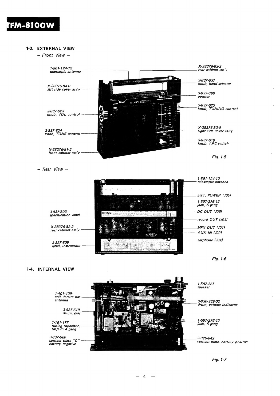
1-3.
External
View
..........cccceceeceeseseerenes
4
4-1.
Resonance
Indicator
Circuit
1-4.
Internal
View
.........cccceesccceeceeeeeeeees
4
Board
...2.c.siccccsseccssesesouasdiveestuedestect
12
4-2.
Vhf
WB
Tuner
Circuit
Board.......
12
2.
DISASSEMBLY
..............ccccccceeceeeeseeeesenees
5
2°
“Main
Gack
Board
2-1.
Rear
Cabinet
Removal
...........cceee
5
—
Conductor
Side
—
................
13
2-2.
Chassis
Removal
Gutiosececaeceuetvesersieeress
5
4-4,
Schematic
Diagram
ae
Nibit
sb
neh
15
2-3.
Printed
Circuit
Board
:
4-5,
Main
Circuit
Board
Removal
sis
iiickteecisteeatdstistete
ined
6
—
Component
Side
—
..........
17
2-4.
Whf
WB
Block
Removal..............
7
2-5.
Dial
Cord
Stringing
.......ccecceeeee
8
S.
EXPLODED
VIEW
AND
PACKING
.....
19
3.
CIRCUIT
ADJUSTMENTS
...0..2...c.cssee.
8
5-1,
Exploded
View
(1)
-....sssseeeeoen
19
;
5-2.
Exploded
View
(2)
.....
cc
eeeeees
21
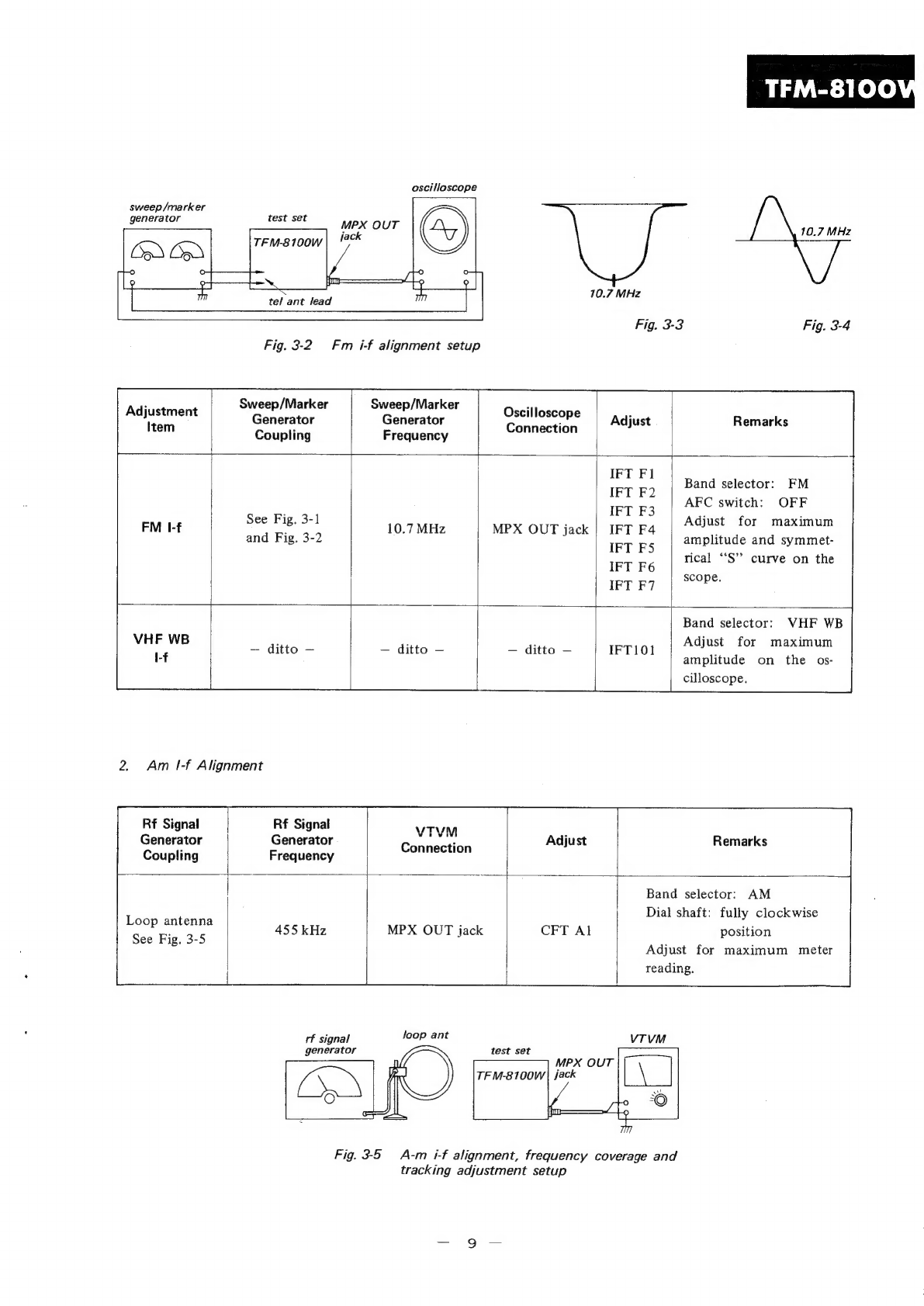
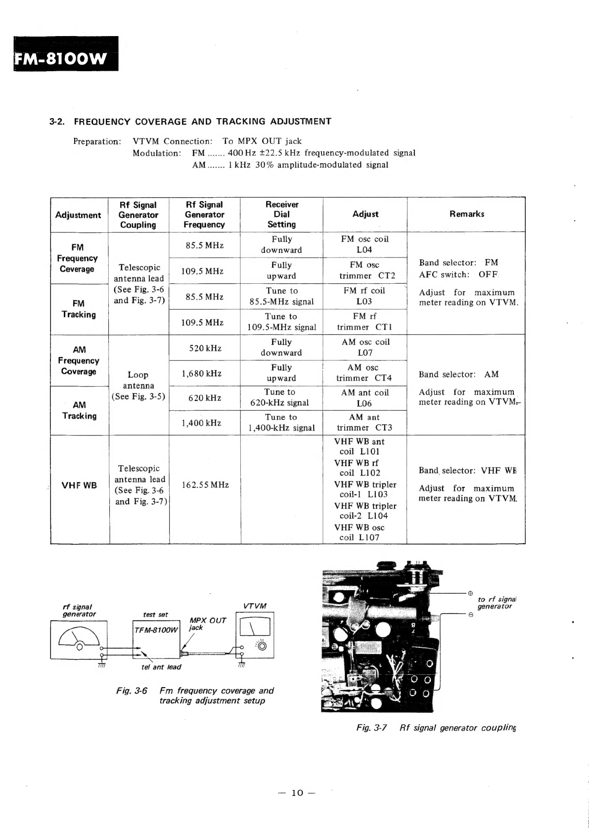
3-1.
Lf
Alignment
....-ssesseessssseesseeseesseeey
8
5-3,
Packing
..c.cecccccccsecsseceseseessecesscescaees
23
3-2.
Frequency
Coverage
and
Tracking
Adjustment
.................05
10
6.
ELECTRICAL
PARTS
LIST
.................
24
SECTION
1
OUTLINE
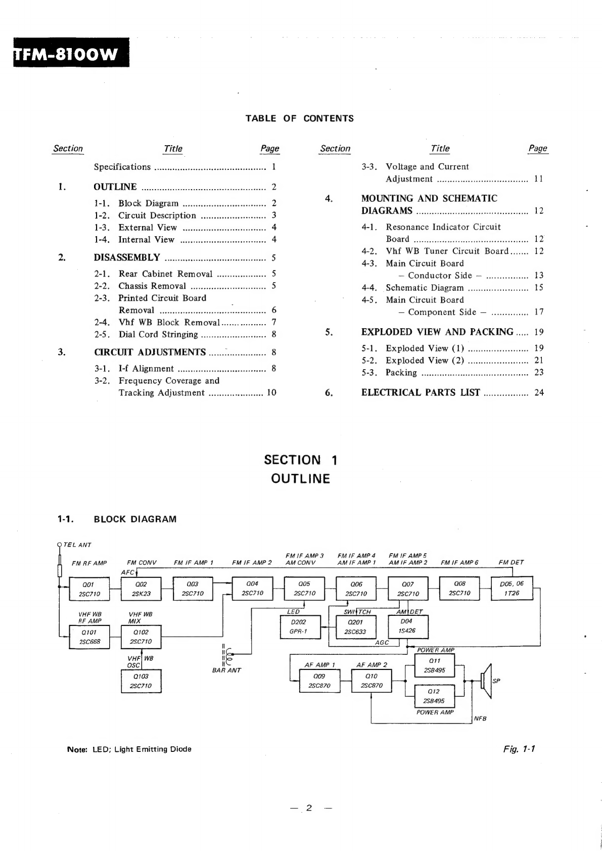
1-1.
BLOCK
DIAGRAM
OTEL
ANT
|
FM
IF
AMP
3
FM
IF
AMP
4
FM
IF
AMP
5
FM
RF
AMP
FM
CONV
FM
IF
AMP
1
FM
IF
AMP
2
AM CONV
AM
IF
AMP
1
AM
IF
AMP
2
FM
IF
AMP
6
FM
DET
AFC
aot
Q02
Q04 Qos Q06
Q07
Q08
DO5,
06
280710
2SK23
2SC710
2SC710
2SC710
28C710
28C710
1726
TCH
RF
AMP
MIX
0202
Q201
p04
Q101
Q102
GPR-1
28C633
18426
'
2SC668
2SC710
;
AGC
Q03
280710
AMIDET.
WG
POWER
AMP
VHF]
WB
We
iF
OSC
ii
AF
AMP
1
AF
AMP
2
BAR
ANT
2SB495
0103
Q0g9
Qio
|
SP
28C710
28C870
2SC870
O12
2SB495
POWER
AMP
NFB
Note:
LED;
Light
Emitting
Diode
Fig,
1-1