Sony PMC-DR50 User manual

Ver 1.0 2000.03
PMC-DR50
SERVICE MANUAL
PERSONAL COMPONENT SYSTEM
SPECIFICATIONS
TAPE Model Name Using Similar Mechanism NEW
Section Tape Transport Mechanism Type MF-PMCDR50
CD Model Name Using Similar Mechanism NEW
Section MD Mechanism Type KSM-213CCP
Optical Pick-up Type KSS-213C
– Continued on page 2 –
US Model
w
w
w
.
x
i
a
o
y
u
1
6
3
.
c
o
m
Q
Q
3
7
6
3
1
5
1
5
0
9
9
2
8
9
4
2
9
8
T
E
L
1
3
9
4
2
2
9
6
5
1
3
9
9
2
8
9
4
2
9
8
0
5
1
5
1
3
6
7
3
Q
Q
TEL 13942296513 QQ 376315150 892498299
http://www.xiaoyu163.com

– 2 –
Specifications ........................................................................... 1
1. SERVICE NOTE........................................................... 3
2. GENERAL ...................................................................... 4
3. DISASSEMBLY
3-1. Case(bottom), “Cover ASSY, Top” .......................... 6
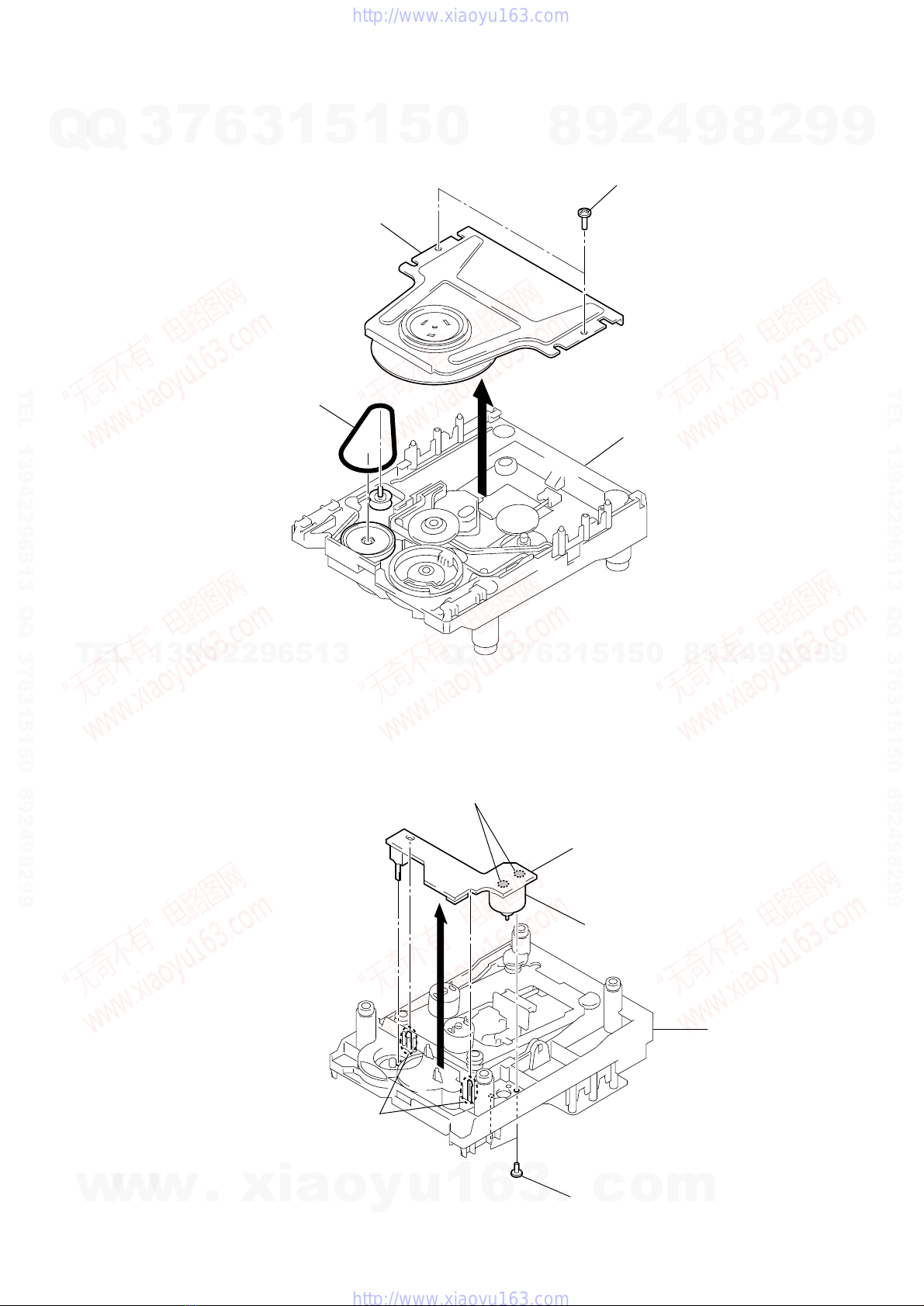
3-2. CD ASSY.................................................................. 7
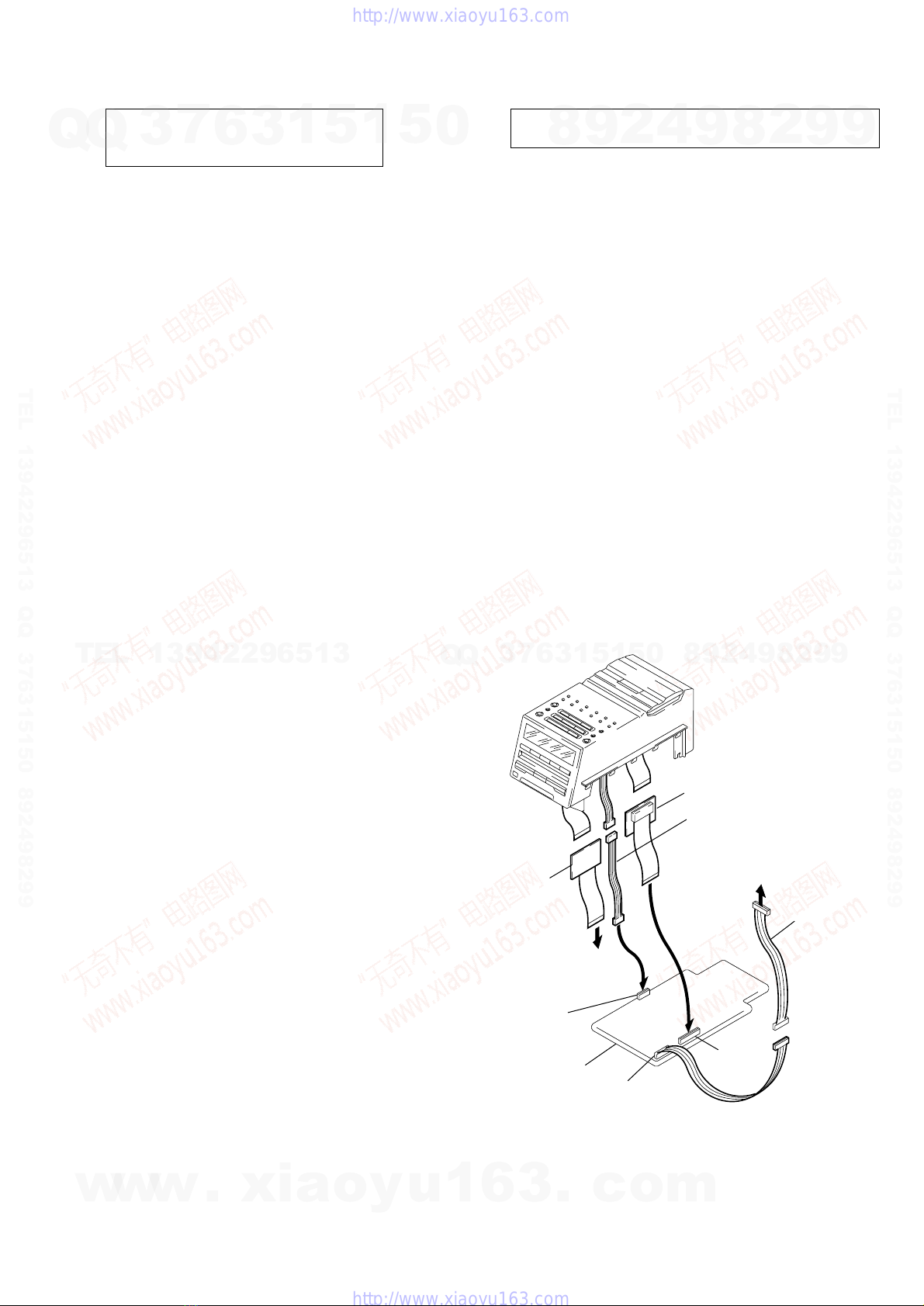
3-3. Main Board, Jack Board ........................................... 7
3-4. Tray ........................................................................... 8
3-5. ASP Board ................................................................ 8
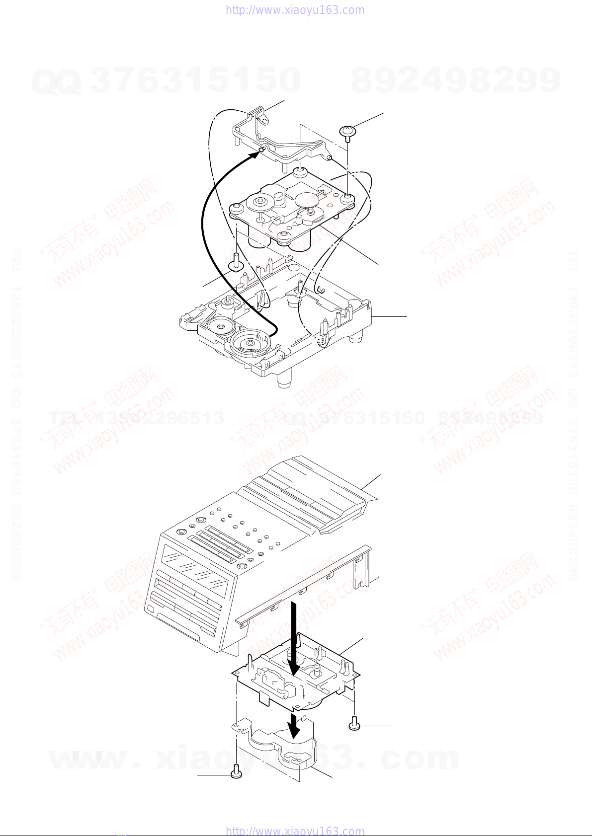
3-6. Belt ........................................................................... 9
3-7. Motor Board, Loading Motor (M651) ...................... 9
3-8. Optical Pick-up Block ............................................ 10
3-9. Mechanism Deck .................................................... 10
3-10. TC RF Board, Head Relay Board,
Capstan/Reel Motor (M160) ...................................11
3-11. Control Board ..........................................................11
3-12. Display Board ......................................................... 12
3-13. DSP Board, CPU board .......................................... 12
3-14. VOL Board ............................................................. 13
3-15. “Cabinet, Wood”, “Cabinet (R) Bottom” ............... 13
3-16. Speaker (R-CH) (SP101) ........................................ 14
3-17. Power Board ........................................................... 14
3-18. AMP Board, AMP IC Board ................................... 15
3-19. Speaker Board ........................................................ 15
4. ADJUSTMENTS
4-1. Mechanical Adjustments........................................... 16
4-2. Electrical Adjustments .............................................. 16
5. DIAGRAMS
5-1. Explanation of IC Terminals................................... 19
5-2. Block Diagrams – CD, Tuner Section – ................. 22
5-3. Block Diagrams – Tape, Main Section– ................. 25
5-4. Printed Wiring Boards – Main Section– ................. 29
5-5. Schematic Diagram – Main Section (1/3) – ........... 33
5-6. Schematic Diagram – Main Section (2/3) – ........... 36
5-7. Schematic Diagram – Main Section (3/3) – ........... 39
5-8. Printed Wiring Boards – CD Section –................... 42
5-9. Schematic Diagram – CD Section – ....................... 45
5-10. Schematic Diagram – Control Section – ................ 49
5-11. Printed Wiring Boards – Control Section – ............ 53
5-12. Printed Wiring Boards – AMP Section – ................ 57
5-13. Schematic Diagram – AMP Section – .................... 59
6. EXPLODED VIEWS
6-1. Case Section ........................................................... 65
6-2. Control Section ....................................................... 66
6-3. CD Mechanism Section .......................................... 67
6-4. Mechanism Deck Section -1................................... 68
6-5. Mechanism Deck Section -2................................... 69
6-6. CD Optical Pick-up Section ................................... 70
6-7. Speaker (R-CH) Section ......................................... 71
6-8. Speaker (L-CH) Section ......................................... 72
7. ELECTRICAL PARTS LIST................................... 73
TABLE OF CONTENTS
w
w
w
.
x
i
a
o
y
u
1
6
3
.
c
o
m
Q
Q
3
7
6
3
1
5
1
5
0
9
9
2
8
9
4
2
9
8
T
E
L
1
3
9
4
2
2
9
6
5
1
3
9
9
2
8
9
4
2
9
8
0
5
1
5
1
3
6
7
3
Q
Q
TEL 13942296513 QQ 376315150 892498299
http://www.xiaoyu163.com

–3 –
NOTES ON HANDLING THE OPTICAL PICK-UP BLOCK
OR BASE UNIT
The laser diode in the optical pick-up block may suffer electrostatic
breakdown because of the potential difference generated by the
charged electrostatic load, etc. on clothing and the human body.
During repair, pay attention to electrostatic breakdown and also use
the procedure in the printed matter which is included in the repair
parts.
The flexible board is easily damaged and should be handled with
care.
NOTES ON LASER DIODE EMISSION CHECK
The laser beam on this model is concentrated so as to be focused on
the disc reflective surface by the objective lens in the optical pick-
up block. Therefore, when checking the laser diode emission, ob-
serve more than 30 cm away from the objective lens.
LASER DIODE AND FOCUS SEARCH OPERATION
CHECK
1. Close the Tray for CD.
2. Press CD ^button.
3. Confirm the laser diode emission while observing the objecting
lens. When there is no emission, Auto Power Control circuit or
Optical Pick-up is broken.
Objective lens moves up and down once for the focus search.
ABOUTTHE EXTENSION CABLE JIG
Extention cable jigs (1-792-164-11, 1-792-165-11, 1-792-223-11
and 1-792-224-11) are necessary when repair this unit.
SECTION 1
SERVICE NOTE
SAFETY-RELATED COMPONENT WARNING!!
COMPONENTS IDENTIFIED BY MARK 0OR DOTTED LINEWITH
MARK 0ON THE SCHEMATIC DIAGRAMS AND IN THE PARTS
LIST ARE CRITICALTO SAFE OPERATION.
REPLACE THESE COMPONENTS WITH SONY PARTS WHOSE
PART NUMBERS APPEAR AS SHOWN IN THIS MANUAL OR IN
SUPPLEMENTS PUBLISHED BY SONY.
Flexible Circuit Board Repairing
•Keep the temperature of the soldering iron around 270°C during
repairing.
•Do not touch the soldering iron on the same conductor of the
circuit board (within 3 times).
•Be careful not to apply force on the conductor when soldering or
unsoldering.
Notes on chip component replacement
•Never reuse a disconnected chip component.
•Notice that the minus side of a tantalum capacitor may be dam-
aged by heat.
Jig (20 core)
(1-792-164-11)
Jig (19 core)(1-792-165-11)
ASP board
(CN702)
Main board
TC RF board
(CN691)
CN804
CN305
CN302
Jig (9 core)
(1-792-224-11
)
Jig (6 pin)(1-792-223-11)
CAUTION
The use of optical instruments with this product
will increase eye hazard.
w
w
w
.
x
i
a
o
y
u
1
6
3
.
c
o
m
Q
Q
3
7
6
3
1
5
1
5
0
9
9
2
8
9
4
2
9
8
T
E
L
1
3
9
4
2
2
9
6
5
1
3
9
9
2
8
9
4
2
9
8
0
5
1
5
1
3
6
7
3
Q
Q
TEL 13942296513 QQ 376315150 892498299
http://www.xiaoyu163.com

–4 –
SECTION 2
GENERAL
LOCATION AND FUNCTION OF CONTROLS
MAIN UNIT
2
4
5
qaq;
ws wa w;
qs
qd
qg
qf
qh
qj
qk
ql
6
7
8
9
1
3
1VOLUME +, –buttons
2CD tray
3Timer buttons
STANDBY
SLEEP
CLOCK
TIMER
DISPLAY
4Display window
5POWER button
6DIMMER button
72(Headphones) Jack
8DIR MODE button
9COUNTER RESET button
!º TAPE operation buttons
r/P(rec/pause)
CD DUBBING
0, )(FF, REW)
ª, ·(play)
π(stop)
!¡ PLAY MODE, MONO/ST ISS button
!™ ENTER/MEM button
!£ =(–) , +(+) TUNE TIME SET button
!¢ LINE IN button
!∞SUMER TIME button
!§ MEGA BASS button
!¶ SOUND button
!• 6CD OPEN/CLOSE button
!ª RADIO operation buttons
PRESET +
BAND
PRESET–
@º CD operation buttons
fl(play/pause)
π(stop)
@¡ SNOOZE button
@™ Remote sensor
w
w
w
.
x
i
a
o
y
u
1
6
3
.
c
o
m
Q
Q
3
7
6
3
1
5
1
5
0
9
9
2
8
9
4
2
9
8
T
E
L
1
3
9
4
2
2
9
6
5
1
3
9
9
2
8
9
4
2
9
8
0
5
1
5
1
3
6
7
3
Q
Q
TEL 13942296513 QQ 376315150 892498299
http://www.xiaoyu163.com

–5 –
Remote commander
1DISPLAY button
2SLEEP button
3POWER button
4Number buttons
5MEGA BASS button
6VOLUME +, –buttons
7SOUND button
8CD operation buttons
=, +(AMS, search)
((play)
P(pause)
p(stop)
9TAPE operation buttons
p(stop)
“, ”(play)
r/P(rec/pause)
0, )(FF, REW)
!º RADIO operation buttons
TUNE +
TUNE –
BAND
!¡ MODE button
HOOKING UPTHE SYSTEM
DISPLAY POWER
CD/RADIO
MODE
RADIO MEGA/BASS VOL
TAPE
SOUND
TUNE
BAND
SLEEP
1 2 3
4
5
6
7
8
9
!º
!¡
w
w
w
.
x
i
a
o
y
u
1
6
3
.
c
o
m
Q
Q
3
7
6
3
1
5
1
5
0
9
9
2
8
9
4
2
9
8
T
E
L
1
3
9
4
2
2
9
6
5
1
3
9
9
2
8
9
4
2
9
8
0
5
1
5
1
3
6
7
3
Q
Q
TEL 13942296513 QQ 376315150 892498299
http://www.xiaoyu163.com

– 6 –
SECTION 3
DISASSEMBLY
Note : Follow the disassembly procedure in the numerical order given.
3-1. CASE (BOTTOM),“COVER ASSY,TOP”
rThe equipment can be removed using the following procedure.
Case(bottom)
Cover ASSY, top
Main unit
CD ASSY Main board, Jack board
Tray ASP board
Motor board, Loading motor (M651) Optical pick-up block
Belt
Mechanism deck TC RF board, Head relay board, Capstan/reel motor (M160)
Control board VOL board
Display board
Cabinet, wood
Speaker unit
(R-CH)
Speaker (R-CH) (SP101) Power board
Cabinet (R) bottom Speaker board
AMP board, AMP IC board
DSP board, CPU board
5Wire, parallel (19 core)
6Wire, parallel (20 core)
(ASP board : CN702)
1Screws (+BVTT 3x10)
4Screws (+KPT 3x10)
37
Case (bottom)
Sub cover
2Claws
2Claws
2Claws
Cover ASSY, top
< MAIN UNIT >
w
w
w
.
x
i
a
o
y
u
1
6
3
.
c
o
m
Q
Q
3
7
6
3
1
5
1
5
0
9
9
2
8
9
4
2
9
8
T
E
L
1
3
9
4
2
2
9
6
5
1
3
9
9
2
8
9
4
2
9
8
0
5
1
5
1
3
6
7
3
Q
Q
TEL 13942296513 QQ 376315150 892498299
http://www.xiaoyu163.com

– 7 –
3-3. MAIN BOARD, JACK BOARD
3-2. CD ASSY
1Screws (+BVTT 3x10)
2
Case (bottom)
CD ASSY
2Screws (+BVTT 2.6x8)
5
3
Case (bottom)
Jack board
Main board
4Screw (+BVTT 2.6x8)
2Screws (+BVTT 2.6x8)
1Screws (+BVTT 3x10
)
w
w
w
.
x
i
a
o
y
u
1
6
3
.
c
o
m
Q
Q
3
7
6
3
1
5
1
5
0
9
9
2
8
9
4
2
9
8
T
E
L
1
3
9
4
2
2
9
6
5
1
3
9
9
2
8
9
4
2
9
8
0
5
1
5
1
3
6
7
3
Q
Q
TEL 13942296513 QQ 376315150 892498299
http://www.xiaoyu163.com

– 8 –
3-4.TRAY
3-5. ASP BOARD
3Projection
2
Tray
3Projection
1Turn the gear in a
direction as a figure
Chassis
3Wire, parallel (16 core)
2Remove solder
1Screw (+P 2x6)
4
Chassis
ASP board
w
w
w
.
x
i
a
o
y
u
1
6
3
.
c
o
m
Q
Q
3
7
6
3
1
5
1
5
0
9
9
2
8
9
4
2
9
8
T
E
L
1
3
9
4
2
2
9
6
5
1
3
9
9
2
8
9
4
2
9
8
0
5
1
5
1
3
6
7
3
Q
Q
TEL 13942296513 QQ 376315150 892498299
http://www.xiaoyu163.com

– 9 –
3-6. BELT
3-7. MOTOR BOARD, LOADING MOTOR (M651)
1Screws (+P 2.6x8)
2
Chassis
Chucking chassis
3Belt
4Loading motor (M651)
1Screws (+B 2x3)
2
Chassi
s
Claws
Motor board
3Remove solder
w
w
w
.
x
i
a
o
y
u
1
6
3
.
c
o
m
Q
Q
3
7
6
3
1
5
1
5
0
9
9
2
8
9
4
2
9
8
T
E
L
1
3
9
4
2
2
9
6
5
1
3
9
9
2
8
9
4
2
9
8
0
5
1
5
1
3
6
7
3
Q
Q
TEL 13942296513 QQ 376315150 892498299
http://www.xiaoyu163.com

– 10 –
3-8. OPTICAL PICK-UP BLOCK
3-9. MECHANISM DECK
2Screws (+PWH 2.6x10
)
4
3
3
Chassis
Optical pick-up block
Arm
1Screws (+PWH 2.6x10)
1Screws (+BVTT 3x10)
3
2
Cover, deck
Cover ASSY, top
Mechanism deck
1Screws (+BVTT 3x10
)
w
w
w
.
x
i
a
o
y
u
1
6
3
.
c
o
m
Q
Q
3
7
6
3
1
5
1
5
0
9
9
2
8
9
4
2
9
8
T
E
L
1
3
9
4
2
2
9
6
5
1
3
9
9
2
8
9
4
2
9
8
0
5
1
5
1
3
6
7
3
Q
Q
TEL 13942296513 QQ 376315150 892498299
http://www.xiaoyu163.com

– 11 –
3-10.TC RF BOARD, HEAD RELAY BOARD, CAPSTAN/REEL MOTOR (M160)
3-11. CONTROL BOARD
6Belt FR
Belt BR Belt FR
7Belt BR
1Screws
4Screw
9
3
5
Capstan/reel motor (M160)
Head relay board
TC RF board
8Screws
2Remove solder
2Remove solder
1Screws (+BVTT 2.6x8)
4
2
Control board
DSP board
CPU board
Cover ASSY, top
3Screws (+BVTT 2.6x8)
w
w
w
.
x
i
a
o
y
u
1
6
3
.
c
o
m
Q
Q
3
7
6
3
1
5
1
5
0
9
9
2
8
9
4
2
9
8
T
E
L
1
3
9
4
2
2
9
6
5
1
3
9
9
2
8
9
4
2
9
8
0
5
1
5
1
3
6
7
3
Q
Q
TEL 13942296513 QQ 376315150 892498299
http://www.xiaoyu163.com

– 12 –
3-12. DISPLAY BOARD
3-13. DSP BOARD, CPU BOARD
3Wire, parallel (19 core)
1Screws (+BVTT 2.6x8)
4
2Wire, parallel (18 core)
Holder, Display PC board
DSP board
Display board
CPU boar
d
7Screws (+BVTT 2.6x8
)
1Screws (+BVTT 2.6x8)
2Support
3
8
5Wire, parallel (18 core)
4Wire, parallel (14 core)
6Wire, parallel (19 core)
DSP board
CPU board
Holder, Display PC board
Display board
w
w
w
.
x
i
a
o
y
u
1
6
3
.
c
o
m
Q
Q
3
7
6
3
1
5
1
5
0
9
9
2
8
9
4
2
9
8
T
E
L
1
3
9
4
2
2
9
6
5
1
3
9
9
2
8
9
4
2
9
8
0
5
1
5
1
3
6
7
3
Q
Q
TEL 13942296513 QQ 376315150 892498299
http://www.xiaoyu163.com

– 13 –
3-14.VOL BOARD
3-15.“CABINET,WOOD”,“CABINET (R) BOTTOM”
3Screws (+BVTT 2.6x8)
2
4
1Claws
Panel ASSY, front
Case (top)
VOL board
1Claws
1Claws
1Claw
s
< SPEAKER UNIT (R-CH) >
2Screws (+P 4x16
)
3
Cabinet, Wood
1Screws (+P 4x16)
Cabinet (R) bottom
Sponge, back board
Note : Change a “Sponge, back board”
(3-042-179-01) for a new article
when remove the cabinet (R) bottom.
w
w
w
.
x
i
a
o
y
u
1
6
3
.
c
o
m
Q
Q
3
7
6
3
1
5
1
5
0
9
9
2
8
9
4
2
9
8
T
E
L
1
3
9
4
2
2
9
6
5
1
3
9
9
2
8
9
4
2
9
8
0
5
1
5
1
3
6
7
3
Q
Q
TEL 13942296513 QQ 376315150 892498299
http://www.xiaoyu163.com

– 14 –
3-16. SPEAKER (R-CH) (SP101)
3-17. POWER BOARD
3
1
Cabinet, Woo
d
2Screws (+BVTT 4x10)
4Screws
Stand, Grill
Stand, Grill
Speaker (SP101)
Speaker grill ASSY
Panel (R) ASSY, Sub
2
Cabinet, Woo
d
1Screws (+P 4x10)
Power board Bracket, Transfomer
Bracket, Transfomer
w
w
w
.
x
i
a
o
y
u
1
6
3
.
c
o
m
Q
Q
3
7
6
3
1
5
1
5
0
9
9
2
8
9
4
2
9
8
T
E
L
1
3
9
4
2
2
9
6
5
1
3
9
9
2
8
9
4
2
9
8
0
5
1
5
1
3
6
7
3
Q
Q
TEL 13942296513 QQ 376315150 892498299
http://www.xiaoyu163.com

– 15 –
3-18. AMP BOARD, AMP IC BOARD
3-19. SPEAKER BOARD
4
2
AMP board
3Screws (3x10)
1Screws (+BVTT 3x12)
Cabinet (R) botto
m
AMP IC board
5
3
2Screws
(+BVTT 3x8)
1Screws
(+BVTT 3x10)
4Screws
(+BVTT 3x8)
Stopper, wire
Cabinet (R) bottom
Stopper, cord
Airtight clipper Bracket
Cord, AC
Cord with connector
Speaker board
6Screws
(+BVTT 3x8)
w
w
w
.
x
i
a
o
y
u
1
6
3
.
c
o
m
Q
Q
3
7
6
3
1
5
1
5
0
9
9
2
8
9
4
2
9
8
T
E
L
1
3
9
4
2
2
9
6
5
1
3
9
9
2
8
9
4
2
9
8
0
5
1
5
1
3
6
7
3
Q
Q
TEL 13942296513 QQ 376315150 892498299
http://www.xiaoyu163.com

– 16 –
SECTION 4
ADJUSTMENTS
4-1. MECHANICAL ADJUSTMENTS
TAPE RECORDER SECTION
PRECAUTION
1. Clean the following parts with a denatured-alcohol-moistened
swab :record/playback/erase head pinch roller
rubber belts capstan
2. Demagnetize the record/playback/erasehead with ahead demag-
netizer.
3. Do not use a magnetized screwdriver for the adjustments.
4. After the adjustments, apply suitable locking compound to the
parts adjusted.
5. The adjustments should be performed with the rated power sup-
ply voltage unless otherwise noted.
Torque Measurement
Torque Torque Meter Meter Reading
Forward CQ-102C 36 to 61 g • cm
(0.5 to 0.84 oz • inch)
Forward CQ-102C 2 to 6 g • cm
Back Tension (0.028 to 0.083 oz • inch)
Reverse CQ-102RC 36 to 61 g • cm
(0.5 to 0.84 oz • inch)
Reverse CQ-102RC 2 to 6 g • cm
Back Tension (0.028 to 0.083 oz • inch)
FF/REW CQ-201B 61 to 143 g • cm
(0.85 to 1.98 oz • inch)
TapeTension Measurement
Mode Tension Meter Meter Reading
FWD CQ-403A more than 100g
(more than 3.53 oz)
REV CQ-403A more than 100g
(more than 3.53 oz)
4-2. ELECTRICAL ADJUSTMENTS
TAPE RECORDER SECTION 0dB = 0.775V
1. The adjustnemts should be performed in the order in the service
manual. (As a general rule playback circuit adjustment should
be completed beforeming recording circuit adjustment.)
2. The adjustments should be performed for bothe L-CH and R-
CH unless otherwise indicated.
Standard Intput Level
Input terminal LINE IN
source impedance 10kΩ
input signal level 0.5V (–3.8dB)
Standard Output Level
Output terminal LINE OUT
load impedance 47kΩ
output signal level 0.5V (–3.8dB)
TestTape
Type Signal Used for
P-4-A100 10kHz, –10dB Azimuth Adjustment
WS-48B 3kHz, 0dB Tape Speed Adjustment
Record/Playback/Erase Head Azimuth Adjustment
Procedure :
1. Mode : FWD playback
2. Turn the adjustment screw for the maximum output levels. If
these levels do not match, turn the adjustment screw until both
of output levels match together within 1dB.
3. Phase Check
Mode : FWD playback
4. Change the reverse playback mode and repeat the step 1 to 3.
5. After the adjustment, lock the adjustment screw with suitable
locking compound.
Adjustment Location : – record/playback/erase head –
set
LINE OUT (JK301
)
47K Ω
level meter
test tape
P-4-A100
(10kHz, –10dB)
L-CH
peak R-CH
peak
L-CH
peak
R-CH
peak
Screw
position
output
level within
1 dB within
1 dB
screw positio
n
VH
in phase 90°
45°135°180°
good wrong
set
L-CH
R-CH
screen pattern
test tape
P-4-A100
(10kHz, –10dB) Osilloscope
LINE OUT (JK301)
47K Ω
47K Ω
adjustment screw
FWD side REV side
w
w
w
.
x
i
a
o
y
u
1
6
3
.
c
o
m
Q
Q
3
7
6
3
1
5
1
5
0
9
9
2
8
9
4
2
9
8
T
E
L
1
3
9
4
2
2
9
6
5
1
3
9
9
2
8
9
4
2
9
8
0
5
1
5
1
3
6
7
3
Q
Q
TEL 13942296513 QQ 376315150 892498299
http://www.xiaoyu163.com

– 17 –
Tape Speed Adjustment
Procedure :
– FWD Playback Mode –
1. Set to FWD playback mode.
2. Adjust RV160 so that the frequency counter reading becomes
3,000Hz.
Standard value : 2,970 to 3,030Hz
3. Set to REV playback mode.
Confirm the frequency should be within the standard value.
4. Confirm the frequency difference between beginning and the
end of tape should be within 1.5% (45Hz).
Adjustment Location : TC RF board
set
test tape
WS-48B
(3kHz, 0dB) frequency counter
LINE OUT (JK301)
47K Ω
TUNER SECTION
AM Section
BAND button : AM
Volume : MIN
FM Section
BAND button : FM
Volume : MIN
• Repeat the procedures in each adjustment several times, and the
frequency coverage and tracking adjustments should be finally
done by the trimmer capacitors.
AM IF ADJUSTMENT
Adjust for a maximum reading on level meter.
T2 450kHz
AM FREQUENCY COVERAGE ADJUSTMENT
Adjust part Frequency display reading on digital
voltmeter.
L5 530kHz Adjustment value :1.4V
Standard value : 1.2 – 1.6V
Confirmation 1,710kHz Standard value : 7.7 – 8.3V
AM TRACKING ADJUSTMENT
Adjust for a maximum reading on level meter.
L4 620kHz
Confirmation 1,400kHz
set
AM RF signal
generator
loop antenna A loop antenna
B
60cm
30% amplitude modulation by 400Hz
signal
Output level : as low as possible
FM RF signal
generator
22.5kHz frequency deviation by
400Hz signal.
Output level : as low as possible
FM EXT.
ANT.
terminal
0.01 µF
set
47K Ω
+
–
LINE OUT (JK301)
level mete
r
0dB=1µV
TC RF board RV160 :Tape speed adjustment
Cabinet, front (Rear side)
w
w
w
.
x
i
a
o
y
u
1
6
3
.
c
o
m
Q
Q
3
7
6
3
1
5
1
5
0
9
9
2
8
9
4
2
9
8
T
E
L
1
3
9
4
2
2
9
6
5
1
3
9
9
2
8
9
4
2
9
8
0
5
1
5
1
3
6
7
3
Q
Q
TEL 13942296513 QQ 376315150 892498299
http://www.xiaoyu163.com

–18 –
FM IF ADJUSTMENT
Adjust for a maximum reading on level meter.
T4 10.7MHz
FM FREQUENCY COVERAGE CONFIRMATION
Adjust part Frequency display reading on digital
voltmeter
Confirmation 87.5MHz 1.2 – 1.6V
Confirmation 108MHz 7.7 – 8.3V
Connect andAdjustment Location :
TP1
+
–
AM frequency coverage
FM frequency coverage
Digital voltmeter
100K Ω
L4 : AM Tracking Adjustment
VT
GND
L5 : AM Frequency coverage Adjustment
T2 : AM IF Adjustment
T4 : FM IF Adjustment
SR1 : Auto Stop Level Adjustment
[MAIN BOARD] (Component side)
FM RF signal
generator
22.5kHz frequency deviation by
400Hz signal.
Output level : 30dBµ
FM EXT.
ANT.
terminal
0.01 µF
1. Set the frequency of FM SSG to 98MHz.
2. Press the TUNE button of the unit to start theAUTO TUNING.
3. Adjustment the SR1 to stop the auto tuning at 30dBµSSG out-
put
Auto Stop Level Adjustment
w
w
w
.
x
i
a
o
y
u
1
6
3
.
c
o
m
Q
Q
3
7
6
3
1
5
1
5
0
9
9
2
8
9
4
2
9
8
T
E
L
1
3
9
4
2
2
9
6
5
1
3
9
9
2
8
9
4
2
9
8
0
5
1
5
1
3
6
7
3
Q
Q
TEL 13942296513 QQ 376315150 892498299
http://www.xiaoyu163.com

– 19 – – 20 –
rCircuit Boards Location.
JACK boar
d
MAIN board
CPU board
VOL board
DISPLAY board
DSP board
HEAD RELAY boar
d
TC RF board
ASP board
MOTOR board
CONTROL board
AMP IC board
POWER board
SPEAKER board
AMP board
MAIN UNIT-1
MAIN UNIT-2
R-CH SPEAKER UNIT
Pin No. Pin name I/O Description
1 G02 O FL grid drive output.
2 G01 O FL grid drive output.
3 NC – Not used (OPEN).
4 CD SCOR I CD SCOR input.
5 T-COUNT I Tape rotation detect input.
6 P.DOWN IN (BACK UP) I Power ON detect input.
7 TAPE AMS IN I AMS signal input.
8 REMOTE IN I Remote control signal input.
9 FM STEREO IN I FM STEREO signal input.
10 RADIO SHFT CLK O Clock shift signal output.
11 LC72131 CE O Radio PLL IC chip enable output.
12 LC72131 CLK O Radio PLL IC clock output.
13 LC72131 DATA IN I Radio PLL IC data input.
14 LC72131 DATA OUT O Radio PLL IC data output.
15 CXD2589Q XRST O CD system reset output.
16 CXD2589Q XLAT O CD DSP IC command latch output.
17 CXD2589Q CLOCK O Clock output for CD DSP IC.
18 CXD2589Q DATA O CD DSP IC command data output.
19 CD OPEN SW IN I CD tray open switch input.
20 CD CLOSE SW IN I CD tray close switch input.
21 CXD2589Q SENS1 I CD SENS input.
22 BU1924F RCLK IN – Not used (OPEN).
23 BU1924F RADIO DATA IN – Not used (OPEN).
24 BU1924F QUARTY IN – Not used (OPEN).
25 CXD2589 SQCK O Clock output for CD SUB-Q.
26 CXD2589 SQSO I CD SUB-Q input.
27 CXD2589 SENS2 I CD SENS input.
28 AVREF I Reference voltage input (for A/D converter).
29-33 KEY1-5 I Key return signal input.
34 TAPE STATUS I Tape detection input.
35 TAPE MECHA MODE SW I FWD/REV detection input.
36 VER I Destination setting terminal (fixed at “H”).
37 AVSS – Ground.
38 RESET I System reset input.
39 EXTAL I O System clock output (8MHz).
40 XTAL1 I System clock input (8MHz).
41 VSS – Ground.
42 XTAL 32.768kHz I Real clock input (32.768kHz).
43 XTAL 32.768kHz O Real clock output (32.768kHz).
44 VDD – Power supply terminal.
45 VFDP – FL power supply terminal.
46 IN I I Initial setting input.
47 CD OPEN OUT O CD tray open signal output.
48 CD CLOSE OUT O CD tray close signal output.
49 PD3 – Not used (OPEN).
50 PD4 – Not used (OPEN).
SECTION 5
DIAGRAMS
5-1. EXPLANATION OF ICTERMINALS
IC801 CXP82832-022Q (SYSTEM CONTROL, FL DRIVE)
– 21 –
Pin No. Pin name I/O Description
51 SYS MUTE O Mute signal output.
52 TUNER MUTE O Tuner mute signal output.
53 CD MUTE O CD mute signal output.
54 LINE MUTE O Line mute signal output.
55 TAPE REC MUTE O Tape mute signal output.
56 TAPE REC O Tape REC output.
57 TAPE BIAS O Tape REC bias select output.
58 TAPE SOL O Plunger control output.
59 TAPE MECHA VCC OUT O Tape mechanism B+ ON/OFF output.
60 ISS 1 O ISS 1 ON/OFF output.
61 ISS 2 O ISS 2 ON/OFF output.
62 MEGABASS O Mega bass ON/OFF output.
63 POWER CONT OUT O Power ON/OFF output.
64 SUMMER LED – Not used. (OPEN)
65 SOUND LED O SOUND LED ON/OFF output.
66 DIMMER LED O DIMMER LED ON/OFF output.
67 BH3854 CK O Clock output for electrical volume IC.
68 BH3854 DATA O Data output for electrical volume IC.
69 BH3854 LACH O LACH output for electrical volume IC.
70 RESERVE – Not used (OPEN).
71-88 SEG 1-18 O FL segment drive output.
89 VDD – Power supply terminal.
90-100 G03-13 O FL grid drive output.
w
w
w
.
x
i
a
o
y
u
1
6
3
.
c
o
m
Q
Q
3
7
6
3
1
5
1
5
0
9
9
2
8
9
4
2
9
8
T
E
L
1
3
9
4
2
2
9
6
5
1
3
9
9
2
8
9
4
2
9
8
0
5
1
5
1
3
6
7
3
Q
Q
TEL 13942296513 QQ 376315150 892498299
http://www.xiaoyu163.com
Other manuals for PMC-DR50
2
Table of contents
Other Sony Speakers System manuals

Sony
Sony HT-A7000 Reference guide

Sony
Sony HT-S400 User manual

Sony
Sony HT-A5000M Reference guide

Sony
Sony SRS-NWM10 User manual

Sony
Sony CMT-ED1A User manual

Sony
Sony SRS-U10 User manual

Sony
Sony SRS-Z500 User manual

Sony
Sony SA-VS150H User manual

Sony
Sony SS-TS5 User manual

Sony
Sony PHC-Z10 Primary User manual