– 11 – – 12 –
SECTION 4
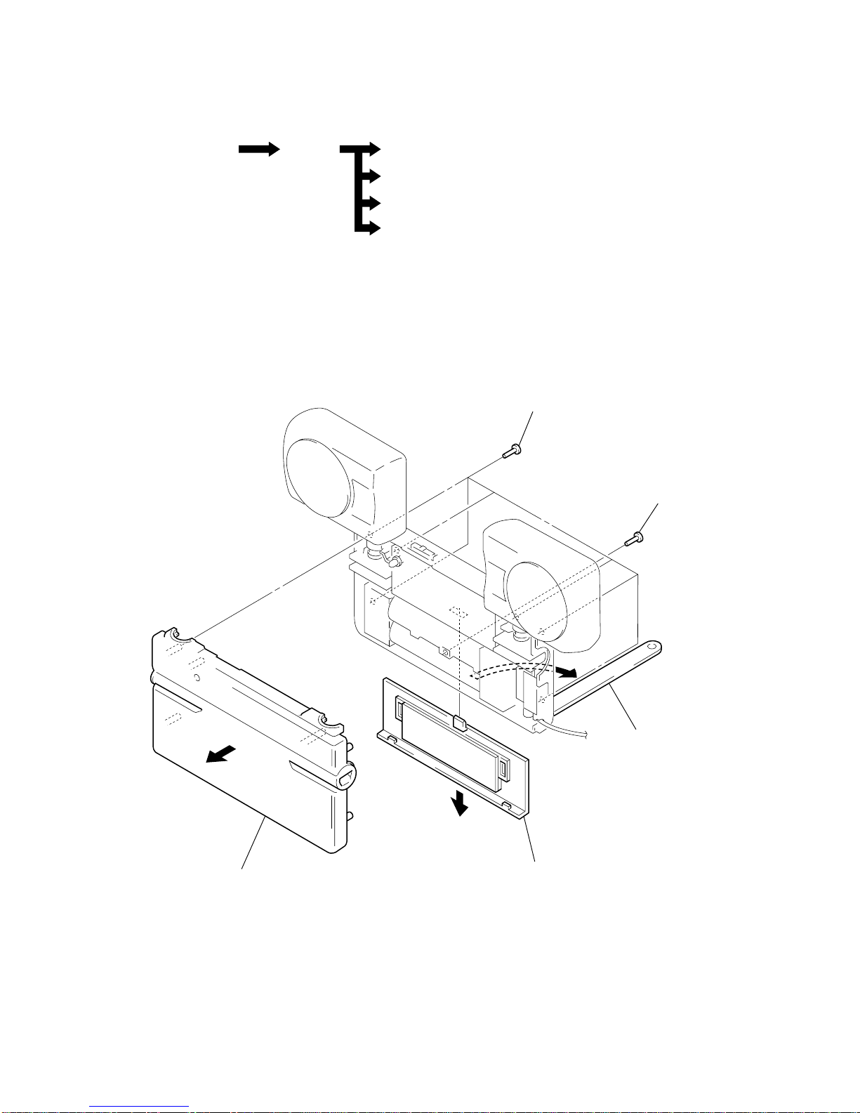
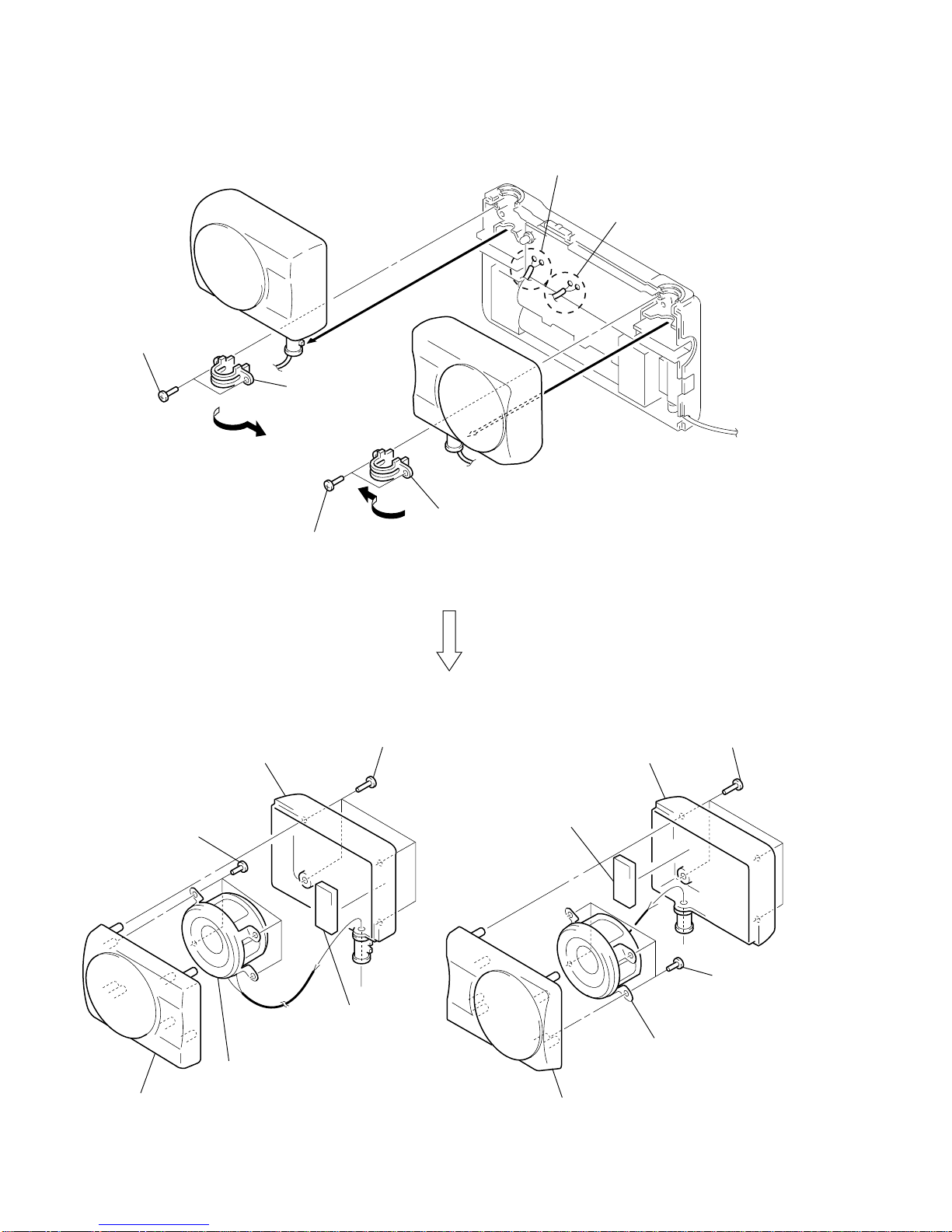
EXPLODED VIEW
• Items marked “*” are not stocked since they
are seldom required for routine service. Some
delay should be anticipated when ordering
these items.
• The mechanical parts with no reference num-
ber in the exploded views are not supplied.
• Hardware (# mark) list and accessories and
packing materials are given in the last of the
electrical parts list.
NOTE:
• -XX and -X mean standardized parts, so they
may have some difference from the original
one.
• Color Indication of Appearance Parts
Example:
KNOB, BALANCE (WHITE) . . . (RED)
↑↑
Parts Color Cabinet's Color
Ref. No. Part No. Description Remark Ref. No. Part No. Description Remark
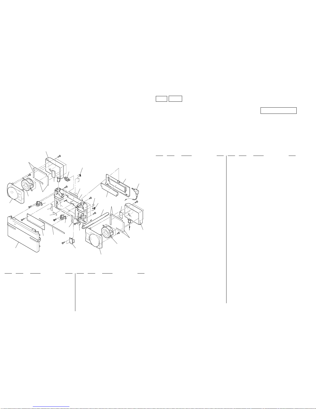
1 4-223-349-01 CASE, FRONT
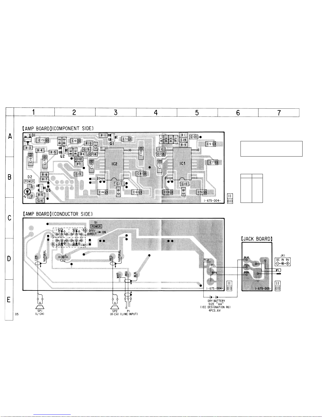
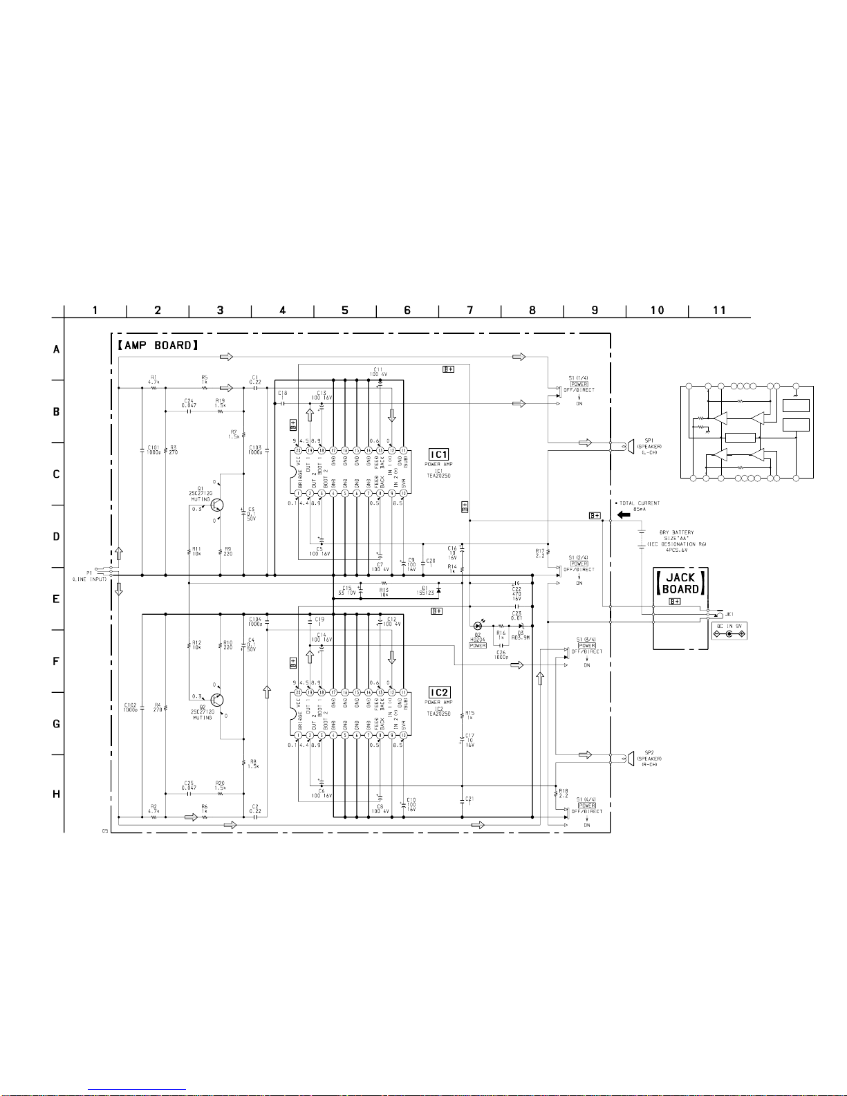
*2 A-4542-603-A AMP BOARD, COMPLETE
3 4-223-357-01 HOLDER, ROTARY SHAFT
4 3-042-545-01 SHEET, BLIND
6 X-4952-281-1 CABINET (L) ASSY, FRONT
7 3-042-547-01 ABSORBENT, ACOUSTIC
8 4-223-355-01 CABINET (L), REAR
9 4-223-348-01 KNOB, SWITCH
10 4-223-361-01 SPRING, BATTERY RELAY
11 4-223-350-01 CASE, REAR
12 4-223-359-01 SPRING, PLUS BATTERY
13 4-223-360-01 SPRING, MINUS BATTERY
14 4-223-358-01 STAND
15 3-042-546-01 CUSHION, BATTERY CASE LID
16 4-223-362-01 LID, BATTERY CASE
17 4-223-356-01 CABINET (R), REAR
18 X-4952-282-1 CABINET (R) ASSY, FRONT
19 4-224-447-01 SPRING, STAND
*20 1-675-005-11 JACK BOARD
21 1-559-891-81 CORD (WITH PLUG)
SP1 1-418-748-11 SPEAKER UNIT (L ch)
SP2 1-418-748-11 SPEAKER UNIT (R ch)
1
2
20
not supplied
#1
#1
#4
#2
#2
#2
#3
#1
#3
#3
#3
#2
not supplied
not supplied
not supplied
SP1
not supplied
not
supplied
21
18
SP2
A
B
B
14
12
13
A
11
15
16
7
10
9
7
8
3
4
4
3419
6
17
SECTION 5
ELECTRICAL PARTS LIST
Ref. No. Part No. Description Remark Ref. No. Part No. Description Remark
AMP JACK
*A-4542-603-A AMP BOARD, COMPLETE
********************
< CAPACITOR >
C1 1-164-222-11 CERAMIC CHIP 0.22uF 25V
C2 1-164-222-11 CERAMIC CHIP 0.22uF 25V
C3 1-126-187-11 ELECT CHIP 0.1uF 20% 50V
C4 1-126-187-11 ELECT CHIP 0.1uF 20% 50V
C5 1-128-397-21 ELECT CHIP 100uF 20% 16V
C6 1-128-397-21 ELECT CHIP 100uF 20% 16V
C7 1-126-209-11 ELECT CHIP 100uF 20% 4V
C8 1-126-209-11 ELECT CHIP 100uF 20% 4V
C9 1-128-397-21 ELECT CHIP 100uF 20% 16V
C10 1-128-397-21 ELECT CHIP 100uF 20% 16V
C11 1-126-209-11 ELECT CHIP 100uF 20% 4V
C12 1-126-209-11 ELECT CHIP 100uF 20% 4V
C13 1-128-397-21 ELECT CHIP 100uF 20% 16V
C14 1-128-397-21 ELECT CHIP 100uF 20% 16V
C15 1-126-393-11 ELECT CHIP 33uF 20% 10V
C16 1-124-779-00 ELECT CHIP 10uF 20% 16V
C17 1-124-779-00 ELECT CHIP 10uF 20% 16V
C18 1-109-982-11 CERAMIC CHIP 1uF 10% 10V
C19 1-109-982-11 CERAMIC CHIP 1uF 10% 10V
C20 1-109-982-11 CERAMIC CHIP 1uF 10% 10V
C21 1-109-982-11 CERAMIC CHIP 1uF 10% 10V
C22 1-126-935-11 ELECT 470uF 20% 16V
C23 1-163-021-11 CERAMIC CHIP 0.01uF 10% 50V
C24 1-163-035-00 CERAMIC CHIP 0.047uF 50V
C25 1-163-035-00 CERAMIC CHIP 0.047uF 50V
C26 1-163-009-11 CERAMIC CHIP 0.001uF 10% 50V
C101 1-163-009-11 CERAMIC CHIP 0.001uF 10% 50V
C102 1-163-009-11 CERAMIC CHIP 0.001uF 10% 50V
C103 1-163-009-11 CERAMIC CHIP 0.001uF 10% 50V
C104 1-163-009-11 CERAMIC CHIP 0.001uF 10% 50V
< DIODE >
D1 8-719-800-76 DIODE 1SS226
D2 8-719-812-43 LED TLG124A (POWER)
D3 8-719-105-57 DIODE RD3.9M-B1
< IC >
IC1 8-759-524-84 IC TEA2025D-013TR
IC2 8-759-524-84 IC TEA2025D-013TR
< TRANSISTOR >
Q1 8-729-230-49 TRANSISTOR 2SC2712-YG
Q2 8-729-230-49 TRANSISTOR 2SC2712-YG
< RESISTOR >
R1 1-216-065-00 RES, CHIP 4.7K 5% 1/10W
R2 1-216-065-00 RES, CHIP 4.7K 5% 1/10W
R3 1-216-035-00 METAL CHIP 270 5% 1/10W
R4 1-216-035-00 METAL CHIP 270 5% 1/10W
R5 1-216-049-11 RES, CHIP 1K 5% 1/10W
R6 1-216-049-11 RES, CHIP 1K 5% 1/10W
R7 1-216-053-00 METAL CHIP 1.5K 5% 1/10W
R8 1-216-053-00 METAL CHIP 1.5K 5% 1/10W
R9 1-216-033-00 METAL CHIP 220 5% 1/10W
R10 1-216-033-00 METAL CHIP 220 5% 1/10W
R11 1-216-073-00 METAL CHIP 10K 5% 1/10W
R12 1-216-073-00 METAL CHIP 10K 5% 1/10W
R13 1-216-073-00 METAL CHIP 10K 5% 1/10W
R14 1-216-049-11 RES, CHIP 1K 5% 1/10W
R15 1-216-049-11 RES, CHIP 1K 5% 1/10W
R16 1-216-049-11 RES, CHIP 1K 5% 1/10W
R17 1-216-298-00 METAL CHIP 2.2 5% 1/10W
R18 1-216-298-00 METAL CHIP 2.2 5% 1/10W
R19 1-216-053-00 METAL CHIP 1.5K 5% 1/10W
R20 1-216-053-00 METAL CHIP 1.5K 5% 1/10W
< SWITCH >
S1 1-554-295-00 SWITCH, SLIDE (POWER)
**************************************************************
*1-675-005-11 JACK BOARD
***********
< JACK >
JK1 1-569-966-11 JACK, DC (DC IN 9V)
**************************************************************
MISCELLAEOUS
*************
21 1-559-891-81 CORD (WITH PLUG)
SP1 1-418-748-11 SPEAKER UNIT (L ch)
SP2 1-418-748-11 SPEAKER UNIT (R ch)
************************************************************
NOTE:
• Due to standardization, replacements in the
parts list may be different from the parts speci-
fied in the diagrams or the components used
on the set.
• -XX and -X mean standardized parts, so they
may have some difference from the original
one.
• RESISTORS
All resistors are in ohms.
METAL: Metal-film resistor.
METAL OXIDE: Metal oxide-film resistor.
F: nonflammable
• Items marked “*” are not stocked since they
are seldom required for routine service.
Some delay should be anticipated when order-
ing these items.
• SEMICONDUCTORS
In each case, u: µ, for example:
uA. . : µA. . uPA. . : µPA. .
uPB. . : µPB. . uPC. . : µPC. .
uPD. . : µPD. .
• CAPACITORS
uF: µF
• COILS
uH: µH
When indicating parts by reference
number, please include the board.